A PCB prototype converts a circuit design into a physical board that can be assembled, measured, debugged, and approved before volume production. It allows engineers to verify electrical performance, component placement, thermal behavior, mechanical fit, and manufacturing feasibility without committing to a large production quantity.
EBest Circuit provides PCB prototype manufacturing for rigid PCB, multilayer PCB, HDI PCB, high-frequency PCB, heavy copper PCB, metal-core PCB, ceramic PCB, flex PCB, and rigid-flex PCB projects. Customers can order bare boards, PCB assembly prototypes, or a turnkey service covering PCB fabrication, component sourcing, assembly, inspection, programming, and functional testing.
Prototype quantities are available for product developers, hardware engineers, start-ups, research teams, OEMs, and purchasing departments. International shipping is available for customers in the USA, Europe, the UK, India, and other markets.
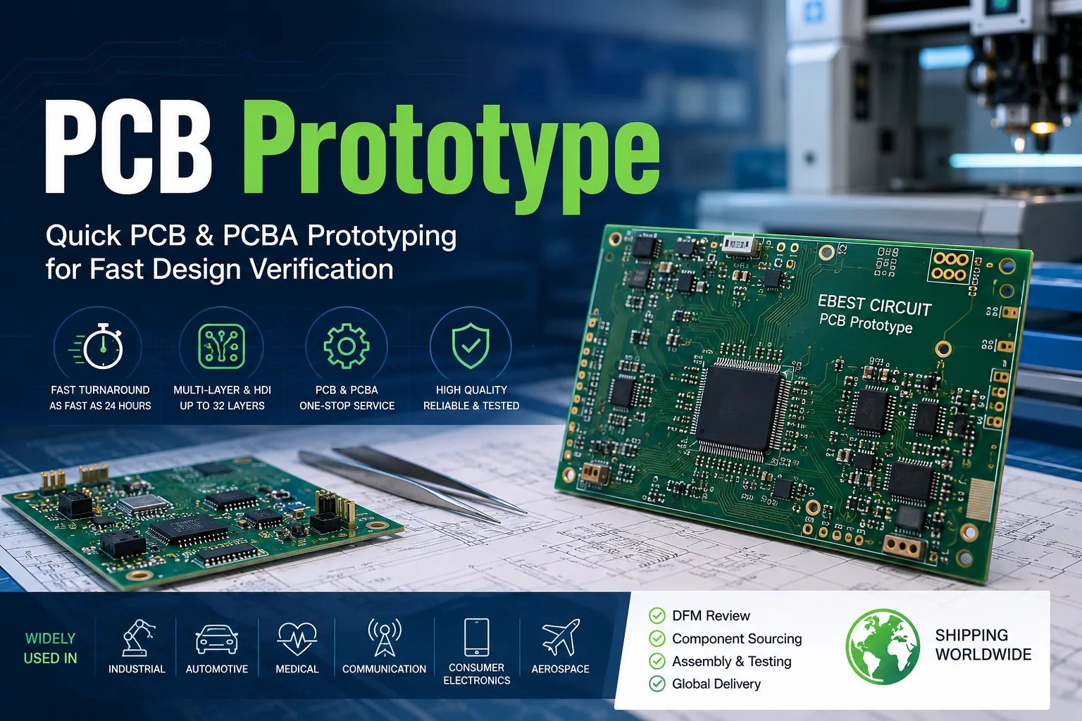
PCB Prototype Services for Fast Design Verification
A prototype should do more than confirm that the circuit powers on. It should reveal whether the design can be manufactured repeatedly, assembled reliably, tested efficiently, and transferred into pilot production.
A PCB prototype can help verify:
- Circuit functionality and signal integrity
- Controlled-impedance performance
- Component package and footprint compatibility
- BGA, QFN, LGA, and fine-pitch assembly
- Thermal distribution and heat dissipation
- Connector alignment and enclosure fit
- Mounting-hole and board-outline accuracy
- Solderability and assembly yield
- Test-point accessibility
- Material suitability
- Firmware and system-level operation
PCB prototype boards may range from a simple 2-layer FR-4 control board to a multilayer HDI PCB, a Rogers hybrid RF board, a thick-copper power PCB, or a fully assembled PCBA prototype.
Before production, the engineering team reviews the Gerber files, drill data, stack-up, impedance requirements, fabrication drawing, BOM, and assembly documents. Any conflict affecting yield, cost, or lead time should be resolved before the manufacturing files are released.
What Is a PCB Prototype?
A PCB prototype design becomes a custom circuit board manufactured in a small quantity for engineering evaluation. It reproduces the intended circuit layout, materials, copper pattern, holes, solder mask, surface finish, board outline, and mechanical features.
It is different from a universal prototype board.
| Product | Structure | Typical Use |
|---|---|---|
| Custom PCB prototype | Manufactured from Gerber or ODB++ data | Functional validation, certification samples, and design verification |
| Universal prototype board | Pre-drilled pads or copper strips | Manual circuit experiments and early concept testing |
| PCB assembly prototype | Custom PCB with components installed | Firmware, thermal, interface, and system testing |
A universal prototype board can be useful during early circuit development. However, it does not reproduce the trace geometry, grounding, impedance, thermal paths, component density, or mechanical dimensions of the final product.
For RF circuits, switching power supplies, high-speed interfaces, dense BGAs, compact products, and controlled mechanical assemblies, a custom PCB prototype is normally required.
PCB Prototype Manufacturing Capabilities
Prototype capability should be assessed as a combination of features rather than by one headline number. Trace width, spacing, copper thickness, drill size, layer count, board thickness, aspect ratio, and via structure influence one another.
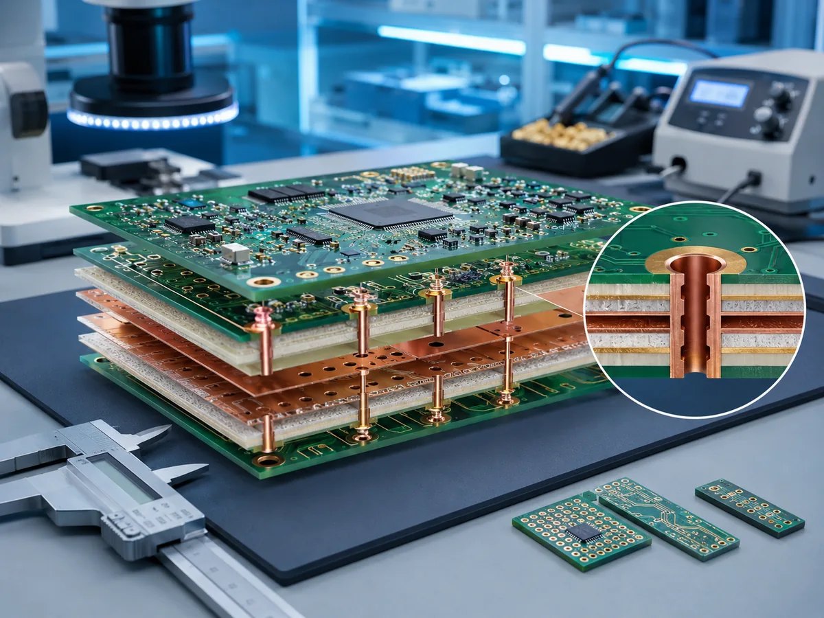
The following table summarizes EBest Circuit’s principal rigid PCB capabilities. Special combinations remain subject to engineering review.
| Manufacturing Item | Standard Capability | Special Capability |
|---|---|---|
| FR-4 layer count | 1–10 layers | Up to 32 layers |
| Inner-layer copper | 0.5–5 oz | Up to 20 oz |
| Outer-layer copper | 1–5 oz | Up to 20 oz |
| Minimum finished mechanical hole | 0.20 mm | 0.15 mm |
| Minimum laser via | 0.10 mm | Project dependent |
| Through-hole aspect ratio | 8:1 | Up to 10:1 |
| Inner-layer trace/space at 0.5–1 oz | 4/4 mil | 3/3 mil |
| Outer-layer trace/space at 1 oz | 4/4 mil | 3/3 mil |
| Common finished thickness range | 0.4–3.5 mm | Approximately 0.15–8.0 mm |
| Outline tolerance | ±5 mil | Approximately ±4 mil |
| Solder mask registration | ±1 mil | Project dependent |
| Maximum conventional FR-4 size | Approximately 600 mm | Long boards by review |
Material options include:
- Standard, mid-Tg, and high-Tg FR-4
- Halogen-free laminate
- Rogers
- Taconic
- Isola
- Nelco
- PTFE-based material
- Hybrid RF and FR-4 constructions
Available surface finishes include:
- Lead-free HASL
- OSP
- ENIG
- ENEPIG
- Immersion silver
- Immersion tin
- Hard gold fingers
- ENIG with hard gold fingers
- Mixed surface finishes by review
A process limit should not automatically become the design rule. For example, 3/3 mil traces may be feasible with light copper, but the same geometry is generally unsuitable for 5 oz, 10 oz, or 20 oz copper.
PCB Prototype Options by Project Type
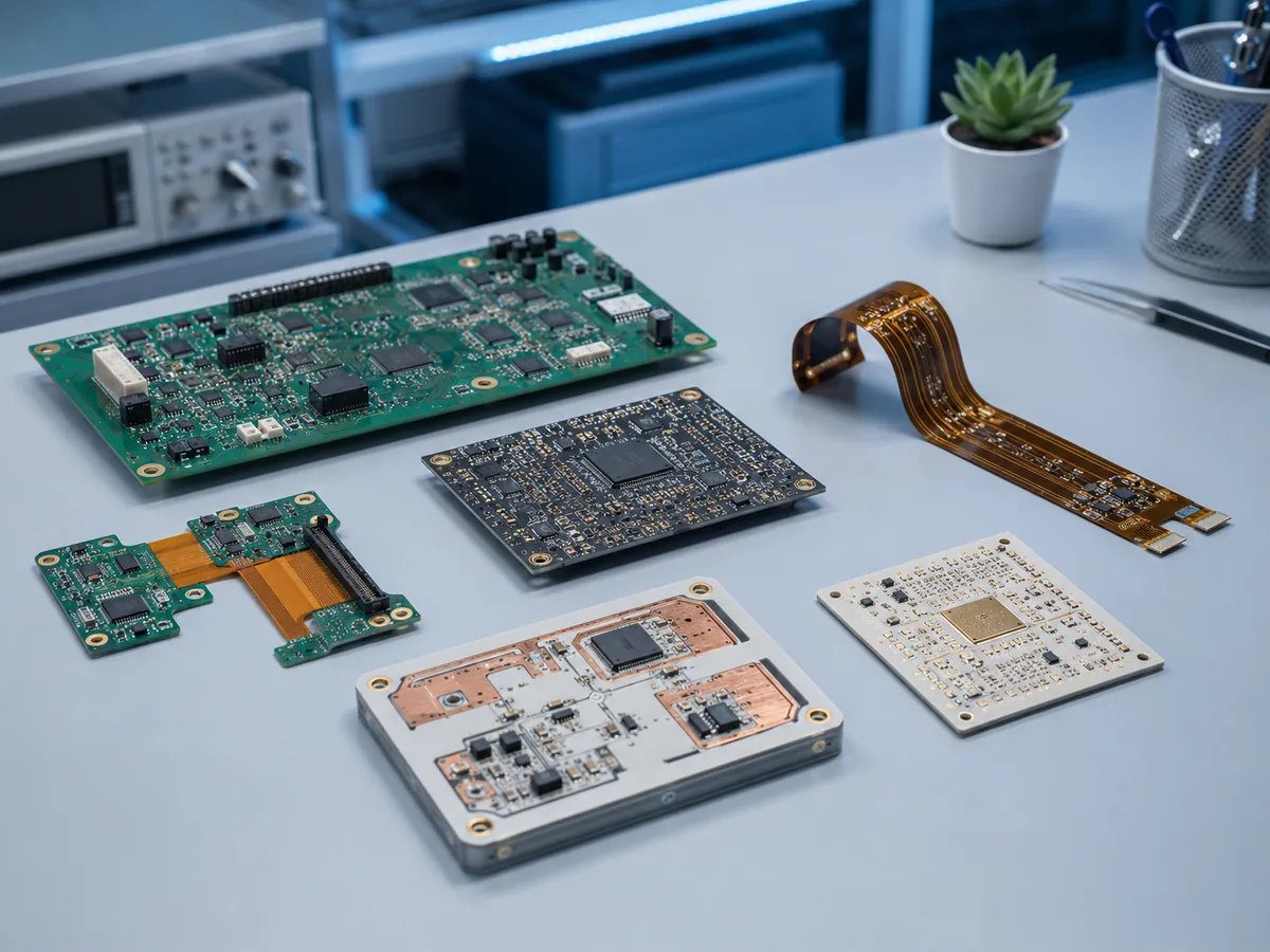
Different PCB technologies require different stack-ups, drilling methods, materials, inspection controls, and lead times. Defining the board type during quotation helps prevent avoidable redesign.
Rigid PCB Prototype
Rigid FR-4 is widely used for industrial controls, embedded systems, consumer electronics, communications equipment, medical devices, automotive modules, and laboratory instruments.
- 1-layer and 2-layer PCB
- Standard multilayer PCB
- Controlled-impedance PCB
- High-Tg PCB
- Thick-board and thin-board PCB
- High-density component layouts
High-Tg material is recommended when the board must withstand demanding lead-free assembly cycles, elevated operating temperatures, or repeated thermal loading.
HDI PCB Prototype
HDI prototypes may use laser-drilled microvias, blind and buried vias, sequential lamination, via-in-pad, stacked or staggered microvias, resin-filled and capped vias, and fine-pitch BGA breakout.
Laser vias down to 0.10 mm and multilayer constructions up to 32 layers are available, subject to stack-up review. The fabrication drawing should identify the intended HDI structure, such as 1+N+1 or 2+N+2.
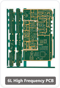
High-Frequency PCB Prototype
Rogers, Taconic, PTFE, Isola, Nelco, and hybrid FR-4 structures are available for RF, microwave, antenna, radar, telecommunications, and high-speed digital applications.
The engineering review should consider design Dk, dissipation factor, dielectric thickness, copper roughness, finished copper thickness, trace geometry, impedance tolerance, surface finish, registration, routing clearance, and hybrid bonding compatibility.
Heavy Copper PCB Prototype
Standard rigid PCB structures support copper weights from 0.5 oz to 5 oz. Special builds can reach 20 oz. Heavy copper designs require greater attention to minimum conductor width, spacing, etching compensation, thermal relief, hole-wall copper, current paths, heat distribution, and finished copper tolerance.
Metal-Core PCB Prototype
Metal-core PCB options include aluminum, copper, and stainless-steel base materials.
| MCPCB Item | Capability |
|---|---|
| Common structures | Single-sided, double-sided, and single-sided two-layer aluminum/copper-base boards; special single-sided four-layer structures by review |
| Finished board thickness | 0.8–3.0 mm standard; 4.0/5.0 mm with special material review; 0.4–1.0 mm for bendable aluminum-base designs |
| Minimum finished PTH | 0.45 mm standard; 0.30 mm subject to engineering evaluation |
| Maximum through-hole aspect ratio | 6:1 |
| Minimum trace/space at 1 oz | 0.20/0.20 mm standard; 0.15/0.15 mm special |
| Maximum processing size | 480 × 1180 mm for standard large aluminum-base panels; special single-sided aluminum-base designs up to 1600 × 480 mm by review |
| Surface finishes | ENIG, ENEPIG, OSP, lead-free HASL |
Metal-core PCBs are commonly used in LED lighting, power converters, motor controls, battery systems, industrial power equipment, and products that transfer heat from the circuit into a metal base.
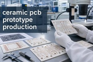
Ceramic PCB Prototype
Ceramic PCB technologies include thin-film, DBC/DCB, DPC, and AMB. Substrate options may include alumina, aluminum nitride, zirconia, and silicon nitride. Material selection should consider thermal conductivity, coefficient of thermal expansion, dielectric performance, copper thickness, mechanical strength, and the intended joining process.
Flex and Rigid-Flex PCB Prototype
Flex and rigid-flex prototypes are used in cameras, sensors, medical devices, wearables, compact modules, moving assemblies, and products that replace wire harnesses or board-to-board connectors.
Quotation files should clearly identify static or dynamic bending, bend location, bend radius, coverlay openings, stiffener details, controlled-impedance areas, component zones, and assembly direction.
Quick PCB Prototype Lead Times
Prototype lead time depends on layer count, material, copper thickness, via structure, surface finish, quantity, inspection requirements, and assembly scope.
| Prototype Type | Typical Lead-Time Approach |
|---|---|
| Basic 1–2-layer FR-4 | Expedited fabrication may be available from approximately 24 hours |
| Standard 4-layer FR-4 | Expedited fabrication may be available from approximately 48 hours |
| Conventional multilayer PCB | Commonly several working days after data approval |
| HDI PCB | Scheduled according to lamination cycles and microvia structure |
| Rogers or hybrid RF PCB | Commonly around 7–10 working days |
| Heavy copper or special material | Confirmed after material and process review |
| PCB assembly prototype | PCB fabrication plus sourcing, assembly, inspection, and testing |
Manufacturing time begins after the production data have been approved and all engineering questions have been resolved. International transportation time is calculated separately.
Lead time can often be reduced by using stocked laminates, standard copper weights, established stack-ups, common solder mask colors, conventional surface finishes, readily available components, and clear manufacturing files.
PCB Assembly Prototype and Turnkey PCBA Services
A bare PCB confirms the physical board construction. A PCBA prototype allows engineers to evaluate the complete electronic assembly, including components, solder joints, firmware, power behavior, interfaces, thermal performance, and system integration.
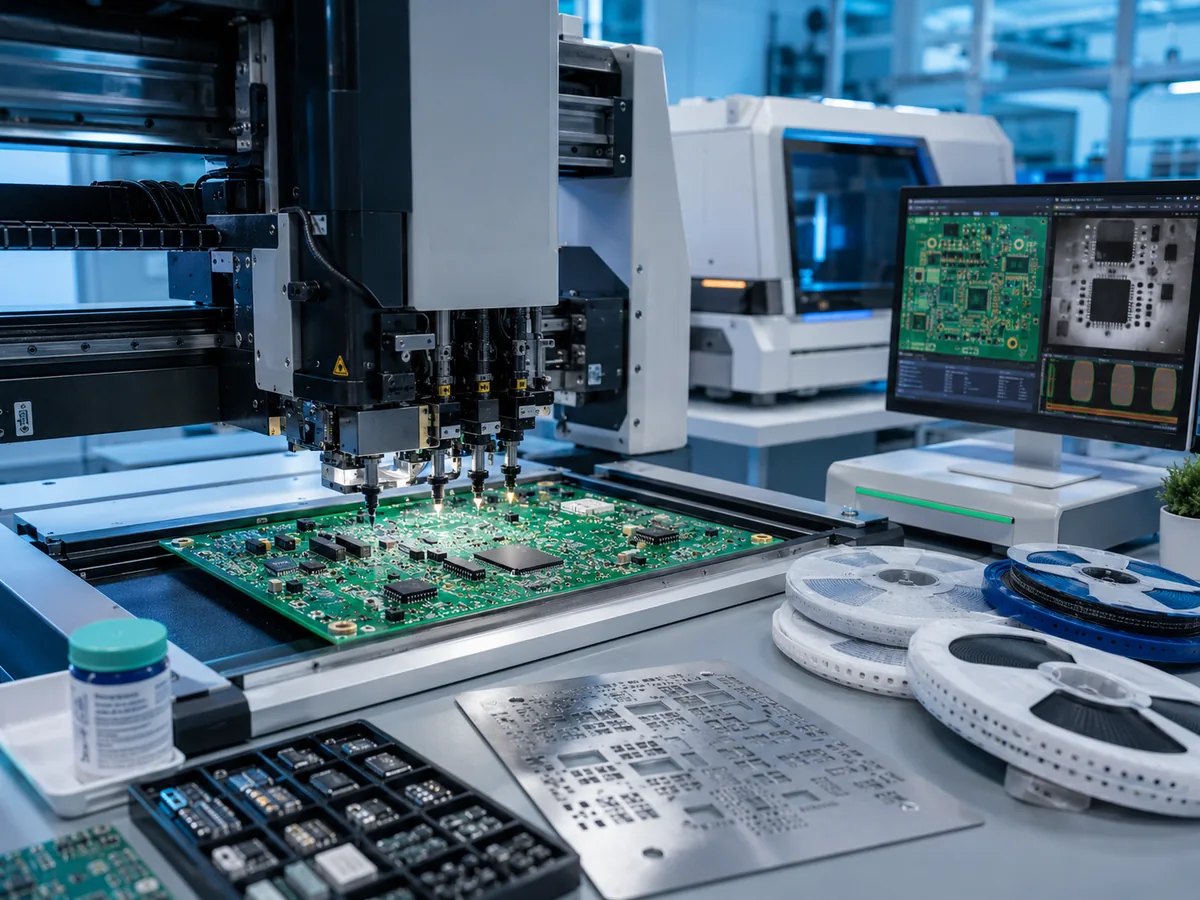
Assembly services can include:
- BOM review and component sourcing
- Alternative-part verification
- SMT and through-hole assembly
- Mixed assembly
- BGA, QFN, LGA, and fine-pitch placement
- Nitrogen reflow and wave soldering
- AOI and X-ray inspection
- ICT support, programming, and functional testing
- Cable assembly and box-build integration
A complete BOM should state the manufacturer, manufacturer part number, description, package, quantity per board, approved alternatives, do-not-fit positions, and special procurement requirements.
PCB Prototype Manufacturing Process
A controlled prototype process keeps the first build useful for design verification and later production transfer.
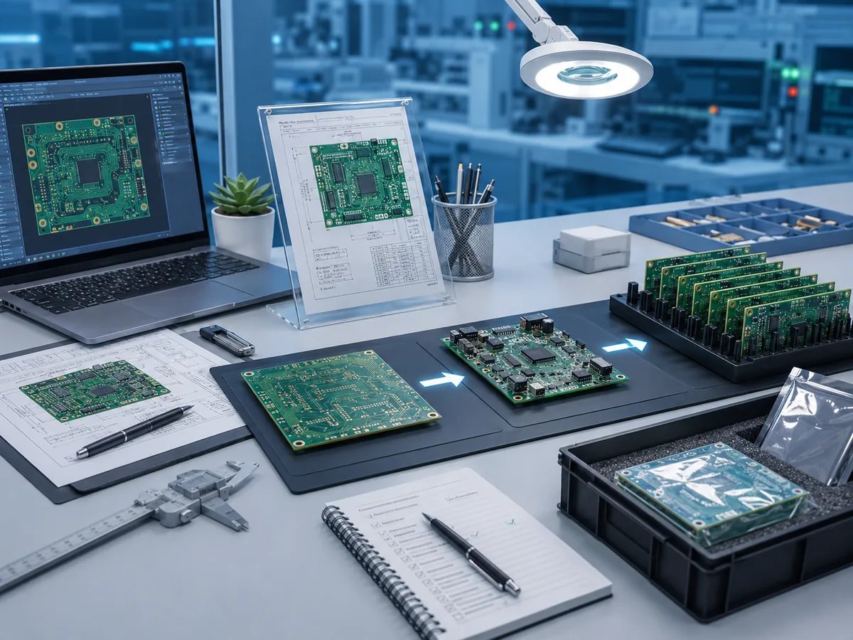
Data Submission
The customer provides Gerber or ODB++ data, drill files, fabrication requirements, quantity, delivery target, and assembly data where applicable.
Engineering and DFM Review
Engineers check layer alignment, trace and spacing, hole size, annular ring, copper-to-edge clearance, solder mask openings, board outline, stack-up feasibility, impedance information, and special process notes.
Material and Stack-Up Confirmation
The laminate, copper weight, dielectric thickness, finished board thickness, surface finish, and special processes are confirmed.
PCB Fabrication
Production may include imaging, etching, lamination, drilling, copper plating, solder mask, surface finishing, routing, scoring, marking, and electrical testing.
Component Sourcing and Assembly
For PCBA projects, components are received, inspected, prepared, placed, soldered, and checked according to the assembly requirements.
Inspection and Testing
Inspection may include bare-board electrical testing, dimensional inspection, SPI, AOI, X-ray, ICT, programming, functional testing, and customer-specific acceptance tests.
Packing and Shipment
Prototype boards and assemblies are protected against moisture, oxidation, electrostatic discharge, and handling damage before shipment.
What Files Are Required for a PCB Prototype Order?
A complete package produces a more accurate quotation and reduces engineering delays.
| File | Required For | Purpose |
|---|---|---|
| Gerber or ODB++ data | PCB fabrication | Defines copper, solder mask, silkscreen, paste, and outline |
| NC drill files | PCB fabrication | Defines plated and non-plated holes |
| Fabrication drawing | Recommended | States material, thickness, copper, finish, and tolerances |
| Stack-up drawing | Multilayer PCB | Defines dielectric and copper construction |
| Impedance table | Controlled-impedance PCB | Lists target values, layers, line types, and tolerances |
| BOM | PCBA | Defines component sourcing requirements |
| Pick-and-place file | PCBA | Provides component coordinates and rotation |
| Assembly drawing | PCBA | Clarifies polarity, orientation, and mechanical details |
| Test procedure | Tested PCBA | Defines test conditions and pass criteria |
| Programming file | Programmed devices | Provides firmware and programming instructions |
A circuit schematic can help with engineering review and functional testing, but it does not replace Gerber or ODB++ manufacturing data.
How Much Does a PCB Prototype Cost?
PCB prototype cost depends on the manufacturing route required by the design. Major cost drivers include layer count, board dimensions, panel utilization, material type, board thickness, copper weight, fine geometry, hole structure, sequential lamination, controlled impedance, surface finish, testing, component availability, assembly complexity, and expedited production.
A cheap PCB prototype is most achievable when the project uses standard FR-4, common thicknesses, moderate copper weight, conventional drilling, standard solder mask, and a widely used surface finish.
Cost reduction should not remove a feature required for meaningful validation. A prototype without the specified impedance, laminate, thermal copper, or inspection process may no longer represent the final product.
How Do You Choose a PCB Prototype Manufacturer?
Check Combined Process Capability
Do not evaluate a manufacturer only by its smallest advertised trace or maximum layer count. Confirm that the required trace width, spacing, copper weight, via type, board thickness, and material can be combined in the same build.
Review the DFM Feedback
Useful DFM feedback should identify the exact issue, the manufacturing or reliability risk, the recommended correction, and the effect on cost or lead time.
Confirm Material Availability
Special laminates can add procurement time. Confirm the exact grade, thickness, copper cladding, and availability before fixing the project schedule.
Match Inspection to the Design
A simple bare PCB may only require electrical and dimensional checks. A dense PCBA may require SPI, AOI, X-ray, programming, and functional testing.
Consider Production Transfer
Changing suppliers after prototype approval may introduce a different stack-up, material source, solder mask process, drilling compensation, or assembly profile. Using one supplier for prototypes, pilot runs, and production reduces transfer risk.
How Do You Move from PCB Prototype to Low-Volume Production?
A successful prototype is one stage of product development rather than the final release.
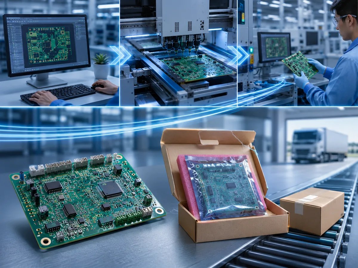
- Engineering validation: Confirm circuit operation, interfaces, firmware, and mechanical fit.
- Design revision: Correct electrical, thermal, EMC, component, or assembly issues.
- Design validation: Test the revised product under intended operating conditions.
- Pilot production: Evaluate assembly yield, fixtures, work instructions, programming, and test coverage.
- Process validation: Confirm that the manufacturing process produces repeatable results.
- Low-volume production: Manufacture controlled quantities for market trials or specialized equipment.
- Volume production: Release the stable design under approved documentation and change control.
Important records should be retained, including the approved stack-up, impedance data, material selection, manufacturing questions, component substitutions, test results, revision history, and released production files.
Why Choose EBest Circuit for PCB Prototyping?
EBest Circuit supports prototype projects that require more than basic bare-board fabrication. Customers can combine rigid, multilayer, HDI, high-frequency, heavy copper, metal-core, ceramic, flex, rigid-flex, and turnkey PCBA services under one project.
The same supplier can support prototype, pilot, low-volume, and volume production. This reduces the need to transfer stack-ups, component data, inspection standards, and process knowledge between manufacturers.
- Free DFM review
- Controlled-impedance engineering
- Component sourcing and alternative-part review
- AOI and X-ray inspection
- Electrical and functional testing
- International delivery
- Order traceability and quality documentation
Frequently Asked Questions
1. What is the difference between a PCB prototype and a prototype board?
A custom PCB prototype is manufactured from the actual circuit design and reproduces the required copper pattern, holes, material, solder mask, finish, and board outline. A universal prototype board contains pre-drilled pads or copper strips for manual circuit experiments.
2. How long does PCB prototype manufacturing take?
Basic 1–2-layer FR-4 boards may qualify for expedited production from approximately 24 hours. Certain 4-layer boards may be available from approximately 48 hours. HDI, RF, heavy copper, ceramic, and assembled projects require additional time.
3. Can I order one PCB prototype?
Yes. Single-piece and small-quantity orders can be reviewed. Several boards are often more practical for assembly setup, debugging, rework, firmware development, and testing.
4. What files are required for a PCB prototype order?
Gerber or ODB++ data and NC drill files are required for fabrication. Multilayer and controlled-impedance projects should also include a stack-up and impedance information. PCBA orders require a BOM, pick-and-place file, and assembly drawing.
5. Do you provide PCB assembly prototype services?
Yes. Services include component sourcing, SMT, through-hole assembly, BGA assembly, AOI, X-ray inspection, programming, functional testing, and box-build integration.
6. How much does a custom PCB prototype cost?
Price depends on layer count, dimensions, material, copper thickness, trace geometry, via structure, surface finish, quantity, testing, assembly complexity, component availability, and lead time.
7. Can a prototype PCB use controlled impedance?
Yes. Controlled impedance is available for multilayer, HDI, high-speed, RF, flex, and rigid-flex projects. Target values and trace types should be clearly identified.
8. Can the prototype move directly into production?
It can move into pilot or production after the design, materials, assembly process, and test results have been approved. A controlled engineering review is recommended before volume release.
9. What tests are performed on prototype PCBs?
Bare-board testing may include continuity and isolation testing, dimensional inspection, impedance testing, and microsection analysis. PCBA inspection may include SPI, AOI, X-ray, ICT, programming, and functional testing.
10. Do you ship PCB prototypes to the USA and Europe?
Yes. Bare PCBs and assembled prototypes can be shipped to the USA, Europe, the UK, India, and other international destinations. Manufacturing and transportation lead times are calculated separately.
How Do You Request a PCB Prototype Quote?
For an accurate quotation, provide Gerber or ODB++ files, NC drill files, a fabrication drawing, quantity, target lead time, BOM and pick-and-place data for assembly, testing requirements, and the delivery destination.
The engineering team will review the data, identify missing information, confirm manufacturing feasibility, and prepare the quotation.
You may also like

Tags: pcb prototype, pcb prototype boards, pcb prototype design, PCB Prototype Manufacturing, pcb prototype service