PCB manufacturing PCB manufacturing
Home > Blog

PCB Quality Control

Industrial PCB Manufacturing Quality Checklist for Buyers
Wednesday, July 15th, 2026
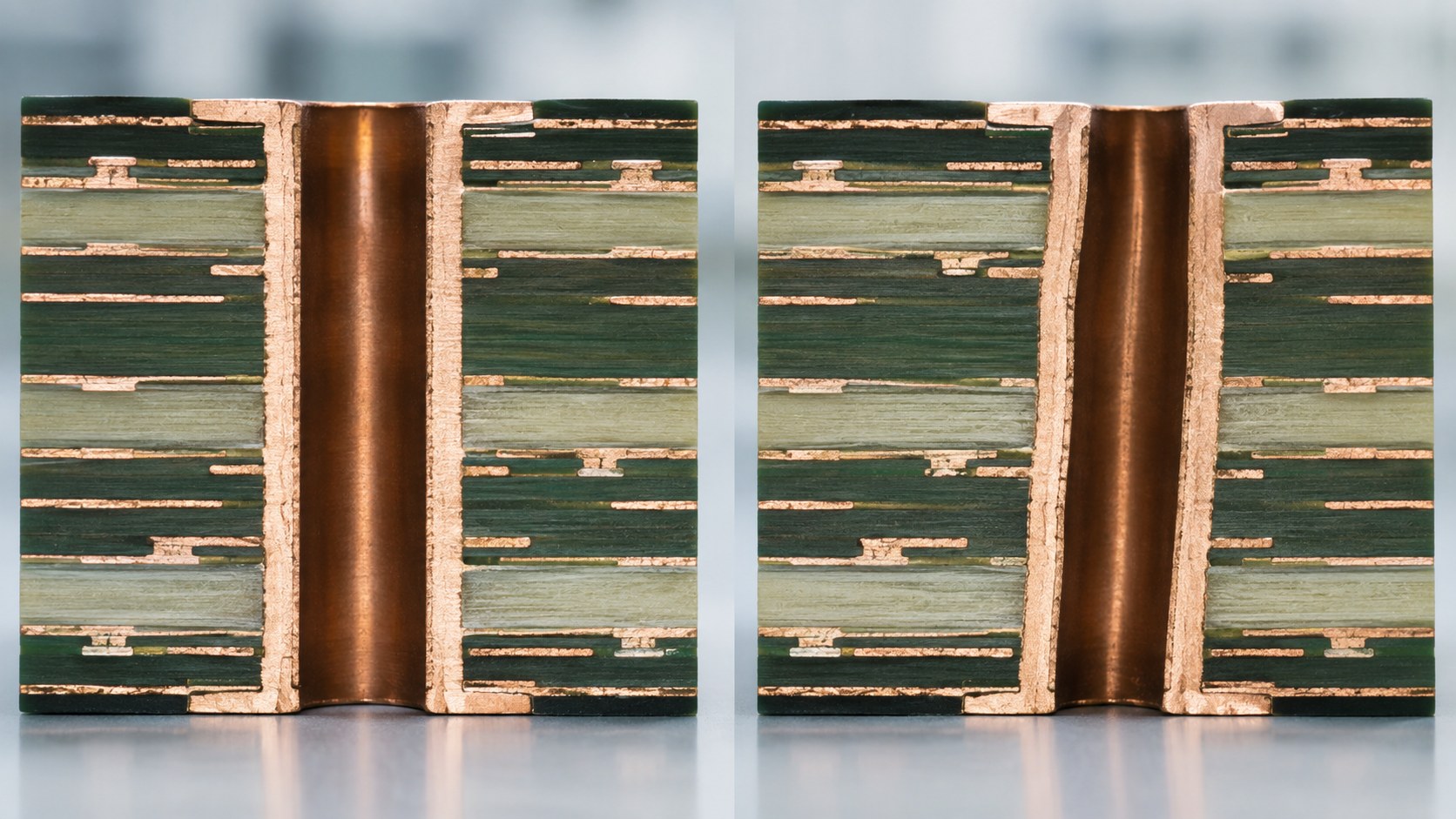
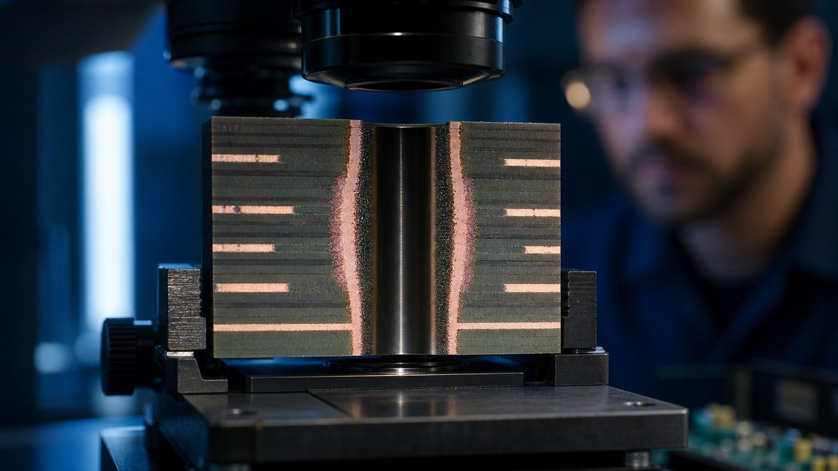
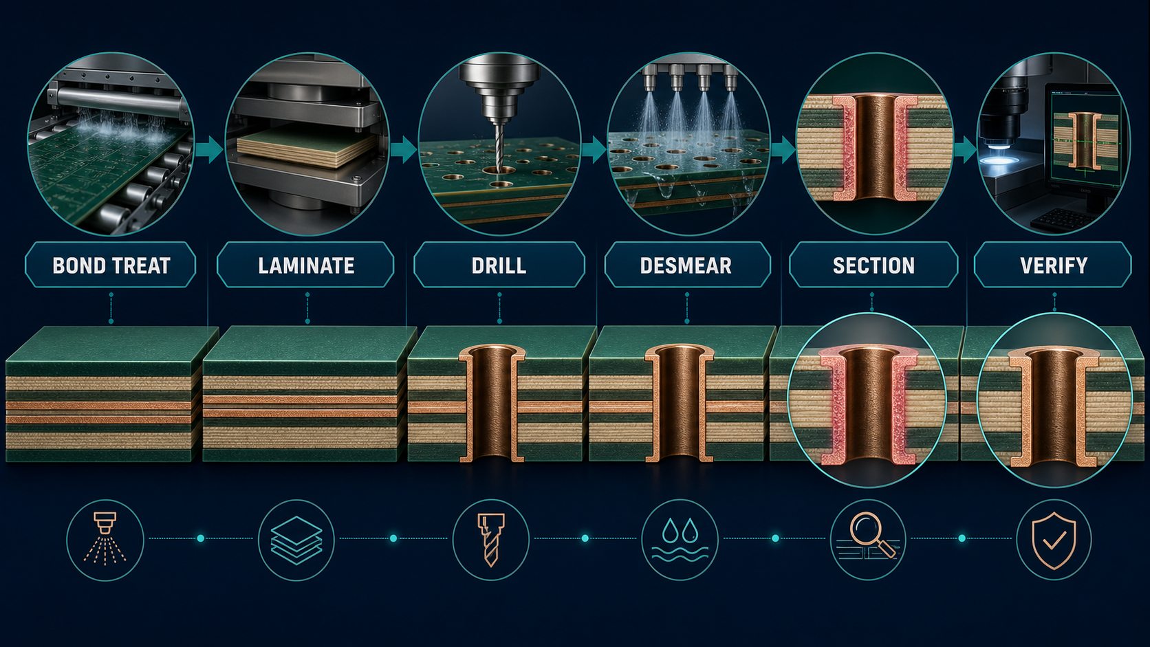
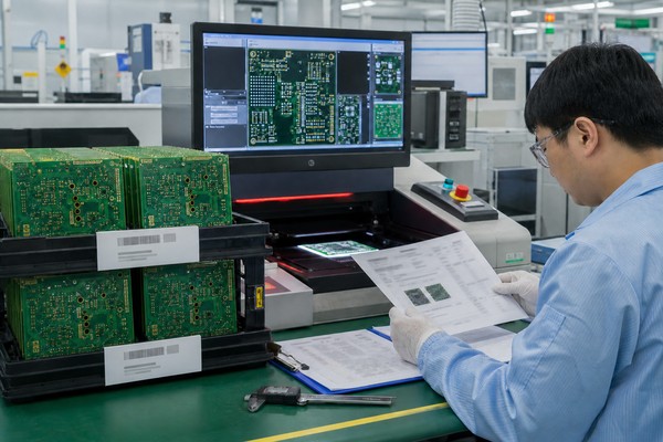
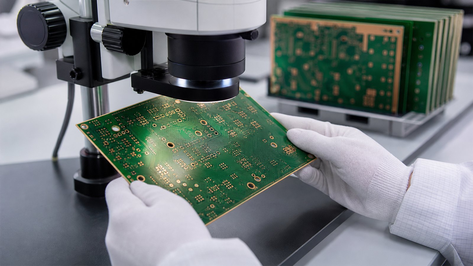
Industrial PCB manufacturing quality review and inspection

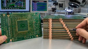
Industrial PCB manufacturing means building circuit boards for equipment where reliability, repeatability, traceability, and production readiness matter more than a simple low-cost board order. For buyers, the useful question is not only how a PCB is made. The better question is what must be checked before an industrial board is released to fabrication, assembly, inspection, and field use.

This guide is written for engineers, purchasing teams, and product teams preparing PCB builds for industrial controls, power modules, automation equipment, test instruments, LED systems, sensors, and embedded electronics. It gives a practical checklist for DFM, material choices, manufacturing files, inspection, supplier questions, and RFQ preparation.

Industrial PCB Manufacturing at a Glance

Industrial PCB manufacturing should connect design review, bare board fabrication, assembly planning, testing, and supplier communication into one controlled workflow. A board may pass a basic electrical test and still create problems if the stackup, thermal path, soldering method, component sourcing, or field environment was not reviewed early.

Area What to confirm Why it matters for industrial projects
Design files Gerber or ODB++, drill file, stackup, notes, drawing Prevents missing data, wrong layer interpretation, and quote delays.
Build requirements Layer count, copper, thickness, surface finish, impedance, material Controls manufacturability, heat, mechanical fit, and repeatability.
Assembly inputs BOM, CPL, polarity, placement notes, special soldering needs Reduces component, orientation, soldering, and rework risk.
Quality control Inspection method, test points, acceptance criteria, packaging Improves consistency before boards reach equipment integration.

When This Manufacturing Checklist Fits Your Project

This checklist fits projects where the PCB must work reliably inside industrial equipment, not only prove a circuit concept on a bench. It is useful when a failed board can stop a machine, create service cost, delay installation, or cause repeated field troubleshooting.

Use it before releasing boards for automation controllers, power conversion modules, control panels, instrumentation, industrial lighting, sensor interfaces, and other equipment that needs stable production. If your project also needs mounted components, compare the PCB build notes with the PCBA and PCB assembly service requirements before sending the RFQ.

Start With the Real Use Environment

The operating environment should guide PCB material, copper, spacing, coating, assembly, and testing decisions before the quote is finalized. Industrial boards may face heat, vibration, current load, dust, humidity, long service life, or maintenance constraints. These conditions can change the safest build approach.

Share the expected operating temperature range, enclosure type, airflow, power load, vibration exposure, connector stress, and installation environment where possible. Avoid turning these into vague notes such as “industrial grade” without explaining what the board must survive.

DFM Review Before Industrial PCB Production

DFM review checks whether the design can be manufactured consistently, inspected properly, and assembled without avoidable process risk. For industrial boards, DFM should happen before the purchase order, not after the supplier has already opened the job.

Important review points include annular ring, drill-to-copper clearance, solder mask bridges, copper balance, panelization, board outline, slot and cutout instructions, edge clearance, component-to-board edge distance, silkscreen clarity, test point access, and thermal copper behavior. The PCB design for manufacturability checklist is a useful supporting guide for the design-side review.

PCB Materials and Stackup Decisions

Material and stackup decisions should match the electrical, thermal, mechanical, and assembly needs of the industrial product. Standard FR-4 can be suitable for many projects, while high-Tg, high-frequency, metal-core, ceramic, flex, rigid-flex, or heavier copper constructions may be needed for specific operating conditions.

Do not rely on a supplier to guess the material path from the Gerber files alone. Provide target board thickness, copper weight, layer count, impedance needs, surface finish, soldering temperature exposure, and any thermal or mechanical constraints. Exact capability limits should be confirmed from the latest Best Technology process capability files before quoting, especially for special materials or non-standard structures.

Copper, Heat and Current-Carrying Requirements

Industrial PCB reliability often depends on whether the copper design, thermal path, and current load are treated as manufacturing requirements instead of late-stage troubleshooting topics. Power traces, connectors, MOSFETs, LEDs, relays, motor control sections, and high-current paths need early review.

For current-heavy or heat-sensitive designs, provide target current, expected temperature rise limits, copper weight expectations, thermal interface notes, enclosure information, and whether the board contacts a heat sink or metal chassis. This helps the supplier identify when heavier copper, wider traces, thermal vias, metal-core material, or layout changes may be needed.

Surface Finish, Solder Mask and Special Processes

Surface finish and special process choices should be selected for assembly method, shelf life, pad geometry, and product environment. The right finish for one prototype may not be the best choice for a production board with fine-pitch components, connectors, or repeated field service.

Decision Buyer question to ask Risk if ignored
Surface finish Does the finish match fine pitch parts, soldering method, shelf life, and cost target? Poor solderability, pad flatness issues, or unnecessary cost.
Solder mask Are mask dams, clearances, and openings suitable for the component pitch? Solder bridging, exposed copper, or inspection confusion.
Special processing Are slots, countersinks, impedance, peelable mask, or selective finish needs documented? Quote revisions and manufacturing holds.

Assembly Planning for Industrial PCB Builds

Assembly planning should connect BOM, CPL, placement drawings, soldering method, inspection access, and test coverage before production starts. Even when the first order is for bare boards, future assembly needs can influence panel design, fiducials, test pads, and connector placement.

For PCB assembly, prepare a clean BOM, CPL, assembly drawing, polarity notes, substitute approval rules, and packaging requirements. If the supplier is also expected to help source components, use the component sourcing service as a reference point for BOM availability, alternates, and purchasing constraints.

Inspection and Testing Requirements

Testing requirements should be defined before the order because industrial PCB quality depends on what is inspected, how defects are caught, and what acceptance criteria apply. A generic “test before shipment” request is not precise enough for many production boards.

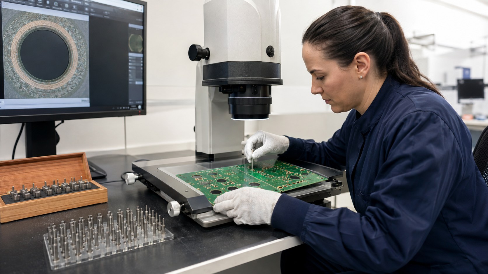
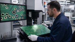
Common checks may include visual inspection, automated optical inspection, electrical test for bare boards, X-ray for hidden solder joints when needed, dimensional checks, and customer-defined functional testing. If functional testing is required, provide the test method, fixture needs, firmware, pass/fail limits, connector access, and safety precautions.

How to Compare Industrial PCB Manufacturing Suppliers

Compare suppliers by their ability to prevent production risk, not only by the lowest unit price. A suitable supplier should ask clarifying questions, flag missing data, explain manufacturing constraints, and document quote assumptions clearly.

  • Can the supplier review Gerber or ODB++ files before production?
  • Can they explain material, finish, copper, and stackup tradeoffs?
  • Can they support both bare board fabrication and assembly when needed?
  • Can they discuss inspection and testing based on the actual board risk?
  • Do they provide clear communication when a requirement needs engineering confirmation?
  • Do they avoid unsupported promises about lead time, certification, or yield?

What Determines Industrial PCB Manufacturing Cost?

Industrial PCB cost is shaped by board complexity, material choice, copper, finish, testing, assembly requirements, quantity, and how complete the RFQ package is. A cheap first quote can become expensive when missing assumptions are corrected later.

Cost factor Why it changes price How to reduce quote uncertainty
Layer count and stackup More layers and controlled builds need more process control. Provide stackup expectations and impedance notes early.
Material and copper Special materials and heavier copper affect sourcing and processing. State material targets, copper weight, and thermal needs.
Surface finish Finish affects assembly, shelf life, pad flatness, and cost. Choose based on component pitch and product needs.
Testing More inspection or functional checks add setup and labor. Define the exact pass/fail criteria and test method.
Assembly and sourcing BOM availability and assembly method affect schedule and price. Send BOM, CPL, approved alternates, and sourcing rules.

Files to Prepare for an Industrial PCB RFQ

A complete RFQ package lets the supplier quote the real project instead of quoting a partial guess. The more industrial risk your board carries, the more important it is to include the build notes and test expectations with the design files.

  • Gerber or ODB++ fabrication data
  • Drill files and board outline drawing
  • Stackup, material, copper, finish, and thickness notes
  • Controlled impedance requirements if applicable
  • BOM, CPL, assembly drawing, and polarity notes for PCBA
  • Quantity, prototype or production stage, and target delivery window
  • Inspection, electrical test, functional test, packaging, and labeling requirements

If you prefer to prepare an online quote package first, the PCB manufacturer online guide explains how buyers can organize the same information before contacting a supplier.

Common Industrial PCB Manufacturing Risks

The most common risks are incomplete files, unclear operating conditions, weak DFM review, BOM uncertainty, unverified special processes, and vague testing requirements. These risks usually appear as quote revisions, production holds, rework, or field issues.

Do not hide uncertainty in short notes. If a requirement is not final, label it as a target and ask the supplier to confirm feasibility. If a component may change, define who approves substitutions. If a board has thermal or vibration exposure, explain the real use case instead of assuming the supplier will infer it from the layout.

Frequently Asked Questions About Industrial PCB Manufacturing

Is industrial PCB manufacturing different from standard PCB fabrication?

Yes. The fabrication steps may look similar, but industrial projects usually need more attention to operating environment, DFM, repeatability, material choices, current load, inspection, and long-term reliability.

Can one supplier handle both PCB manufacturing and assembly?

Yes, when the supplier supports both fabrication and PCBA. A combined path can reduce handoff problems because Gerber, BOM, CPL, assembly notes, and testing requirements can be reviewed together.

What should I send for an industrial PCB quote?

Send Gerber or ODB++, drill files, stackup notes, material and finish requirements, quantity, target schedule, and any testing or packaging requirements. For assembly, also send BOM, CPL, and assembly drawings.

Should I choose the cheapest industrial PCB supplier?

Not automatically. Low price is useful only when the quote includes the real material, process, inspection, assembly, and testing requirements. Compare assumptions before comparing unit price.

Final RFQ Recommendation

Before placing an industrial PCB manufacturing order, prepare the files and risk notes that let the supplier review the project as a real production build. A strong RFQ package should include Gerber or ODB++, drill data, stackup, material, copper, finish, BOM, CPL, drawings, quantity, testing requirements, packaging notes, and target delivery timing.

For an engineering review or quotation, send your Gerber or ODB++ files, BOM, CPL, mechanical drawings, quantity, material expectations, surface finish, test requirements, and target lead time to sales@bestpcbs.com. The Best Technology / bestpcbs team can review the manufacturing path, confirm what needs project-specific checking, and help you prepare the next industrial PCB build without relying on hidden assumptions.

You may also like

AOI in PCB Manufacturing and PCBA Quality Control
Wednesday, July 15th, 2026
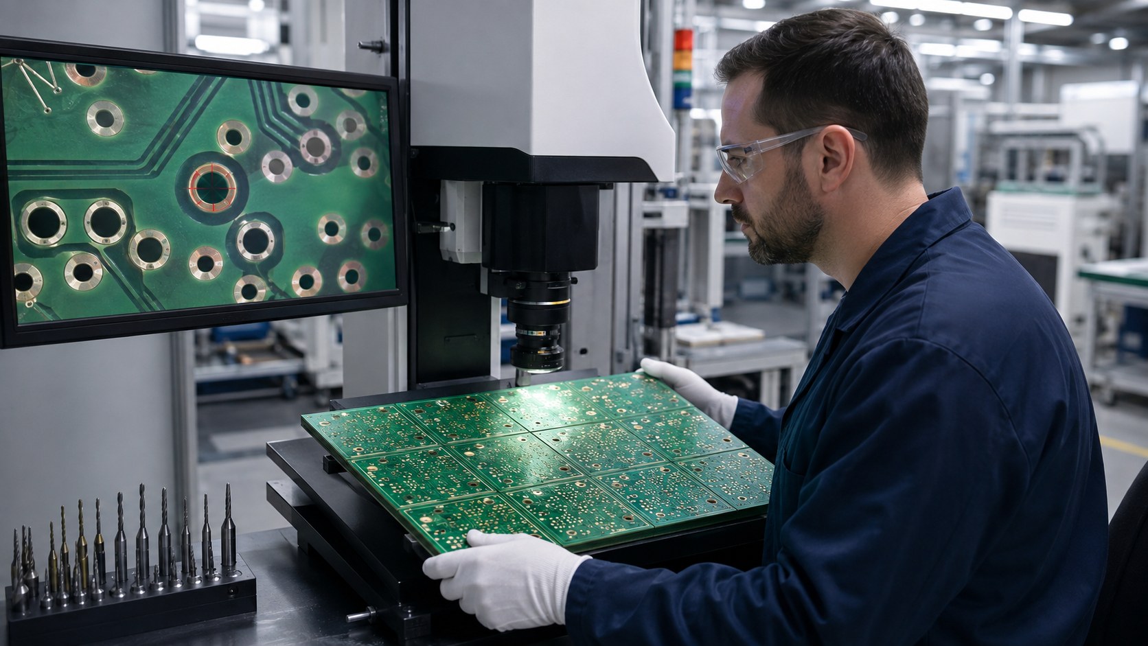
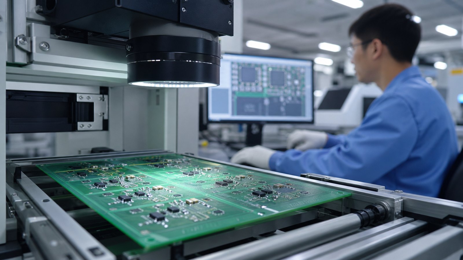
AOI in PCB manufacturing inspection system

AOI in PCB manufacturing means automated optical inspection: a camera-based inspection process used to find visible defects on bare PCBs or assembled PCBAs before they move to the next production step. It helps manufacturers catch issues such as missing components, wrong polarity, solder defects, bridging, insufficient solder, misalignment, surface damage, and certain pattern defects, but it does not replace every electrical, X-ray, or functional test.

This guide explains where AOI fits in PCB and PCBA quality control, what it can detect, what it cannot prove, and what buyers should ask before sending an RFQ for production or assembly.

AOI in PCB Manufacturing at a Glance

AOI is a fast visual inspection method that compares PCB or PCBA images against programmed inspection rules. It is useful because many defects are visible before the board reaches final testing.

Inspection point AOI can help check AOI cannot fully replace
Bare PCB Pattern defects, solder mask issues, surface contamination, open or short risk clues Full electrical testing and final acceptance criteria
SMT assembly Missing parts, wrong polarity, offset, tombstoning, visible solder defects Hidden solder joint X-ray or powered functional testing
Final PCBA Visible assembly defects and workmanship consistency Firmware, load, signal, thermal, or application-specific tests

Where AOI Fits in the PCB Production Flow

AOI is usually placed after a manufacturing or assembly step where visible defects should be caught before more value is added to the board. In SMT assembly, AOI is commonly used after solder paste and reflow-related steps depending on the process plan. In bare PCB manufacturing, optical inspection can help flag pattern or surface issues before later processing.

For buyers, the important question is not simply whether AOI exists. Ask where it is used, which defect types are checked, and whether findings are reviewed by trained staff before boards are released.

What AOI Can Detect on PCBAs

AOI is strongest at detecting visible component and soldering problems on assembled boards. It is especially useful when there are many SMT parts and manual visual inspection would be slow, inconsistent, or easy to miss.

  • Missing, shifted, skewed, or rotated components
  • Wrong polarity on LEDs, diodes, ICs, or capacitors when markings are visible
  • Solder bridges and visible insufficient solder
  • Tombstoning, lifted leads, and package placement issues
  • Surface contamination or visible damage

For assembled projects, AOI should connect with the broader PCBA service workflow rather than standing alone as a checkbox.

What AOI Can Detect on Bare PCBs

For bare boards, optical inspection can help identify visible pattern, solder mask, silkscreen, and surface issues before shipment or assembly. It may flag scratches, contamination, missing features, copper pattern problems, solder mask misregistration, or visual abnormalities that need review.

AOI is only one layer of control. Bare-board electrical testing, process control, material verification, and final inspection still matter, especially for boards with fine features, controlled impedance, high current, or special materials.

AOI vs SPI, X-Ray and Functional Testing

AOI checks visible features, SPI checks solder paste, X-ray checks hidden structures, and functional testing checks whether the circuit works under defined conditions. These tests answer different questions.

Method Best for Typical limit
SPI Solder paste volume and print quality before placement Does not prove final component function
AOI Visible placement and solder defects Cannot see every hidden joint or prove circuit function
X-ray BGA, QFN, hidden solder joints, voiding review Not usually needed for every simple board
Functional test Power, signal, firmware, application behavior Requires buyer-defined test plan or fixture

AOI Limits Buyers Should Understand

AOI reduces visual defect risk, but it does not guarantee that every board will pass electrical or application testing. It depends on the inspection program, image quality, board design, component markings, operator review, and whether the defect is visible to the camera.

Hidden BGA solder joints, internal layer issues, marginal electrical behavior, thermal performance, firmware problems, and intermittent failures may require other test methods. Buyers should define the risk level and ask which inspection combination is appropriate.

How AOI Supports DFM and Process Feedback

AOI findings can feed back into DFM and process improvement when recurring defects point to pad design, stencil, placement, soldering, or component issues. If the same defect appears repeatedly, the supplier should not only sort boards. They should investigate the cause.

Examples include solder bridging caused by pad spacing, tombstoning caused by land pattern imbalance, weak polarity markings, or recurring placement offsets. This is why quality control should connect to engineering review before repeated production.

AOI for SMT, Through-Hole and Mixed Assembly

AOI is most common in SMT inspection, but mixed assemblies still need a planned inspection approach. Through-hole parts, connectors, large components, and hand-soldered features may need visual inspection, selective process checks, or functional testing in addition to AOI.

For through-hole-heavy projects, review the assembly route and inspection plan before quoting. The through-hole assembly page can be useful when a project combines SMT and mechanical-strength components.

What Buyers Should Ask About AOI Before RFQ

Buyers should ask what AOI checks, when it is used, what defect criteria apply, and what other tests are needed for the product. A supplier that only says “AOI included” has not given enough information for a high-risk board.

  • At which production stages is AOI used?
  • Which defect types are programmed for this board?
  • Are AOI findings reviewed before release?
  • Does this board need X-ray because of BGA, QFN, or hidden joints?
  • Does the buyer need to provide firmware, fixtures, or functional test requirements?

Cost and Lead-Time Impact of AOI

AOI can add inspection steps, but it often reduces downstream rework risk for assemblies with many components or visible soldering risk. The impact depends on board complexity, production volume, inspection program setup, and whether other tests are also required.

For quote planning, include test and inspection expectations early instead of adding them after the price is approved. The custom PCB cost guide can help buyers understand why inspection and testing should be treated as cost factors, not afterthoughts.

RFQ Checklist for AOI and PCB Quality Control

An RFQ should define the board files, assembly files, component risk, and inspection expectations clearly enough for the supplier to recommend the right quality plan.

  • Gerber or ODB++ files and drill data
  • BOM and CPL if assembly is required
  • Assembly drawing, polarity notes, and test point requirements
  • Package types such as BGA, QFN, fine-pitch ICs, connectors, or LEDs
  • Required inspection: AOI, X-ray, electrical testing, programming, or functional testing
  • Acceptance criteria and known product risks

Frequently Asked Questions

What does AOI mean in PCB manufacturing?

AOI means automated optical inspection. It uses cameras and programmed inspection rules to identify visible defects on bare PCBs or assembled PCBAs.

Can AOI replace functional testing?

No. AOI checks visible defects. Functional testing checks whether the circuit works under defined electrical or application conditions. Many projects need both.

Is AOI needed for every PCB assembly?

Not always. It is most valuable when there are many SMT components, fine-pitch packages, polarity-sensitive parts, or higher reliability requirements. Simple boards may need a lighter inspection plan.

Does AOI find BGA solder defects?

AOI can inspect visible features around BGA placement, but hidden solder joints usually require X-ray or another suitable inspection method.

What should I send if I need AOI and testing?

Send Gerber or ODB++ files, BOM, CPL, assembly drawing, package notes, test requirements, firmware or fixture needs, quantity, and acceptance criteria.

Send PCB Inspection and Assembly Requirements

If your PCB or PCBA project needs AOI, X-ray, functional testing, or a defined quality-control plan, send your Gerber or ODB++ files, BOM, CPL, assembly drawing, package details, quantity, and test requirements to the Best Technology / bestpcbs engineering team at sales@bestpcbs.com. The team can review which inspection steps fit the board design, assembly risk, and shipment requirements before production starts.

You may also like

Billboard Defect in SMT: Is Your PCBA Supplier Controlling It Properly?
Thursday, May 21st, 2026

Billboard defect in SMT is a side-standing chip component defect that happens when a resistor, capacitor, or other small SMD part does not lie flat on the PCB pads after reflow soldering. The part may still touch the pads, but the solder joint is not formed in the correct position. This can raise concerns about electrical contact, mechanical strength, IPC acceptance, and long-term PCBA reliability.

This article explains what billboard defect in SMT means, how it differs from tombstone defect, whether it can be accepted under IPC workmanship standards, why it happens, and how a professional PCBA supplier should inspect and prevent it. The goal is not only to explain the defect, but also to help engineers, buyers, and quality teams judge whether their SMT assembly process is being controlled properly.

EBest Circuit (Best Technology) provides PCB fabrication, component sourcing, SMT assembly, PCBA manufacturing, testing, and box-build assembly support for customers from prototype to mass production. If you are preparing a PCB or PCBA project and want to reduce SMT assembly risks before production, please contact us at sales@bestpcbs.com.

billboard defect in smt

What Is Billboard Defect in SMT?

Billboard defect in SMT happens when a chip component stands on its side instead of lying flat on the PCB pads. The part looks like a small signboard, so this defect is often called billboarding or side stand.

It often appears on small chip resistors and capacitors. It is more common with 0402, 0201, and 01005 parts. These parts are light, small, and easy to move during solder reflow.

A billboarded part may still touch the pads. So, the board may pass a basic electrical test. But this does not mean the solder joint is reliable.

The contact area may be small. The solder joint may be weak. The part may fail later during vibration, heat cycling, handling, or final product use.

That is why a PCBA supplier should not treat billboard defect as a simple visual issue. It needs proper inspection, root cause analysis, and process control.

billboard defect in smt

Billboard Defect vs Tombstone Defect: What Is the Difference?

Billboard defect and tombstone defect are often confused. Both can happen during SMT assembly, but they are different defects.

ItemBillboard DefectTombstone Defect
AppearanceComponent stands on its sideOne end lifts from the pad
Common nameSide standDrawbridge
Electrical riskMay still conductOften causes an open circuit
Main concernWeak solder jointDirect functional failure
Typical judgmentNeeds further reviewUsually more serious

A tombstone defect usually means one end of the component has lifted away from the pad. This often creates an open circuit.

A billboard defect may still have contact with the pads. However, the solder joint is not formed as designed. The board may work during testing, but the joint may not survive long-term use.

This difference matters. A supplier should not mix these two defects in a quality report. The wrong defect name can lead to the wrong corrective action.

billboard defect in smt

Is Billboard Defect in SMT Acceptable Under IPC Standards?

IPC-A-610 is widely used to judge PCBA workmanship. It helps define what is acceptable, what is a process indicator, and what is a defect.

However, billboard defect should not be judged by one simple rule. The final decision depends on several factors:

  • Product class
  • Customer standard
  • Component size
  • Defect quantity
  • Solder contact condition
  • Mechanical strength
  • Circuit function
  • Product application

For example, a low-risk consumer product and a medical control board should not be judged in the same way. Automotive, aerospace, medical, industrial, and communication products often need stricter control.

A key point is this: passing an electrical test does not always mean the defect is acceptable.

A billboarded part may still conduct electricity. But if the solder joint is weak, it can become a field failure risk.

A responsible supplier should provide clear evidence before asking the customer to accept the board. Useful evidence includes AOI images, defect location, affected quantity, IPC judgment basis, test results, and corrective action.

Why Does Billboard Defect Happen During SMT Assembly?

Billboard defect usually comes from imbalance. The imbalance may come from PCB design, solder paste, placement, reflow, or material quality.

Uneven pad design

  • If one pad connects to a large copper area and the other pad connects to a thin trace, both sides heat at different speeds. One end may wet faster than the other. This can pull the part into the wrong position.

Unbalanced solder paste volume

  • If one pad gets more solder paste than the other, the solder force becomes uneven. Small chip parts can rotate, lift, or stand on their side during reflow.

Poor stencil design

  • Stencil openings control solder paste volume. If the aperture size or shape is not suitable, the paste deposit may become unbalanced. This is a common risk for small passive components.

Placement offset

  • Small SMT parts need accurate placement. If the part is not centered on both pads, reflow may not correct the position. In some cases, it can make the defect worse.

Unsuitable reflow profile

  • A fast heating rate or short soak time can create uneven wetting. One side may melt and pull first, while the other side is not ready. This can cause billboarding or tombstoning.

Poor solderability

  • Oxidized component terminals or PCB pads can also cause uneven wetting. Old parts, poor storage, or exposed reels may increase this risk.

How to Find the Root Cause of Billboard Defect in SMT?

A good PCBA supplier should not only say, “This is an SMT issue.” They should find the real cause.

Area to CheckWhat It May Show
PCB designUneven pads, large copper connection, missing thermal relief
Stencil designUneven solder paste volume
Solder paste printingPaste offset, paste height issue, poor release
Placement processOffset, wrong nozzle, feeder instability
Reflow profileFast ramp rate, weak soak stage, uneven heating
Material conditionOxidation, poor solderability, bad storage
AOI dataRepeated defect at the same location

The most useful question is:

Is this an isolated defect or a repeated process problem?

If the same location fails again and again, the issue may come from pad design, copper balance, or stencil opening.

If the defect appears randomly, the cause may be paste printing, placement, reflow, or material control.

This matters because it helps define the next action. A design issue may need a Gerber change. A printing issue needs stencil or process adjustment. A solderability issue needs material review.

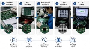
How Can EBest Circuit (Best Technology) Inspect Billboard Defect Before Shipment?

EBest Circuit (Best Technology) uses several inspection steps to reduce the risk of SMT defects before shipment.

First article inspection

  • Before batch production, we check component value, position, polarity, orientation, and soldering condition. This helps find problems before they affect the full lot.

AOI inspection

  • AOI is one of the main tools for finding billboard defect in SMT production. It can detect side-standing parts, missing parts, offset, skew, polarity errors, solder bridging, and poor solder joints.

Manual visual inspection

  • For uncertain AOI results, trained inspectors review the board with magnification and proper lighting. This helps confirm real defects and reduce false calls.

X-Ray inspection

  • X-Ray is mainly used for hidden solder joints, such as BGA, QFN, and LGA. For normal chip resistors and capacitors, AOI and visual inspection are usually more direct. Still, X-Ray is important for full PCBA quality control when hidden joints are present.

ICT and FCT testing

  • ICT and FCT can find open circuits, shorts, wrong values, and function problems. But they cannot replace visual inspection.

A billboarded component may pass electrical testing. Yet the solder joint may still be weak. That is why visual inspection and electrical testing should work together.

billboard defect in smt

How Does Billboard Defect Affect Electrical Performance and Long-Term Reliability?

Billboard defect may not cause instant failure. That is why it can be risky.

A side-standing part may still conduct. But the solder joint is not normal. The contact area may be small, and the joint may have lower strength.

This can lead to:

  • Higher contact resistance
  • Unstable electrical contact
  • Weak mechanical strength
  • Solder joint cracking
  • Failure during vibration
  • Failure after thermal cycling
  • Open circuit during field use

The risk is higher in products that face heat, vibration, shock, or long service life. This includes automotive electronics, industrial controllers, medical devices, outdoor equipment, power products, and communication systems.

So the right question is not only:

Does the board work now?

The better question is:

Will the board stay reliable in real use?

How Can SMT Assembly Prevent Billboard Defect from Happening Again?

Prevention should start before SMT production. A reliable supplier should control both design and process factors.

DFM review

  • Check pad size, pad symmetry, copper balance, solder mask opening, and component spacing. If one pad connects to a large copper area, thermal relief may be needed.

Stencil optimization

  • Control solder paste volume on both pads. For small chip components, more paste is not always better. Balanced paste is more important.

Stable paste printing

  • Control stencil cleaning, squeegee pressure, printing speed, paste condition, and PCB support. Good printing helps reduce solder imbalance.

Accurate placement

  • Use the correct nozzle, feeder setup, component library, and placement data. Small parts need tighter placement control.

Proper reflow profile

  • Avoid heating too fast. Give both sides of the component enough time to reach a balanced temperature. Adjust the profile based on board thickness, copper area, and component density.
Material control

  • Store PCBs and components correctly. Prevent oxidation and moisture issues. Review old or exposed components before production.

AOI trend review

  • AOI should not only catch defects. It should also help engineers find patterns. If the same location fails again, the team should review design, stencil, placement, and reflow together.

Why Choose EBest Circuit (Best Technology) for Reliable SMT Assembly and PCBA Manufacturing?

Customers searching for billboard defect in SMT usually need more than a definition. They need a supplier who can prevent the issue, inspect it, explain it, and fix it.

EBest Circuit (Best Technology) provides one-stop PCB and PCBA manufacturing support. Our services include PCB fabrication, component sourcing, SMT assembly, through-hole assembly, testing, and box-build assembly.

We support customers from prototype to mass production. Our team can review Gerber files, BOMs, assembly drawings, and test requirements before production.

Our PCBA support includes:

  • DFM review before production
  • PCB fabrication and PCBA assembly
  • Component sourcing support
  • SMT process control
  • AOI, X-Ray, ICT, and FCT testing
  • Engineering support for defect analysis
  • Prototype and batch production support
  • Quality control for demanding applications

For billboard defect, tombstone defect, solder bridging, poor wetting, and other SMT issues, our team reviews the issue from design, material, and process angles.

This helps customers reduce repeat defects, improve shipment quality, and build more reliable electronic products.

To sum up, billboard defect in SMT is not only a small visual issue. It can reflect pad design imbalance, solder paste variation, placement offset, reflow profile problems, or material solderability issues. For PCBA projects, the best approach is to prevent this defect before production through proper DFM review, stable SMT process control, and reliable inspection.


If your next PCB or PCBA project requires careful SMT assembly control, EBest Circuit (Best Technology) can support your project from early manufacturing review to final assembly and testing. To discuss your PCB fabrication or PCBA assembly requirements, contact us at sales@bestpcbs.com.

FAQs About Billboard Defect in SMT

1. Is billboard defect the same as tombstoning?

No. Billboard defect means the component stands on its side. Tombstoning means one end lifts from the pad. Tombstoning usually has a higher open-circuit risk.

2. Can a billboarded component pass electrical testing?

Yes. It may still touch the pads and pass testing. But the solder joint may still be weak. Visual inspection and reliability review are still needed.

3. Is billboard defect acceptable under IPC-A-610?

It depends on product class, component size, quantity, location, customer standard, and actual solder condition. The supplier should provide inspection evidence before making a judgment.

4. What causes billboard defect in SMT?

Common causes include uneven pad design, poor stencil design, unbalanced solder paste, placement offset, poor reflow profile, and weak solderability.

5. Which components are more likely to have billboard defect?

Small chip resistors and capacitors are more likely to have this defect. 0402, 0201, and 01005 packages need careful process control.

6. Can billboard defect be repaired?

Yes. Skilled technicians can repair it with proper tools and controlled heating. After repair, the board should go through visual inspection and electrical testing again.

7. How can a PCBA supplier prevent billboard defect?

The supplier should use DFM review, proper stencil design, stable solder paste printing, accurate placement, suitable reflow profile, and AOI inspection.

8. Why should customers care if the board still works?

Because the solder joint may be weak. The board may pass testing now but fail later during vibration, heat cycling, handling, or field use.

9. What should I ask my PCBA supplier about this defect?

Ask for the defect location, inspection images, IPC judgment basis, root cause, affected quantity, repair plan, and prevention action.

If you are preparing a PCB or PCBA project and want to reduce SMT assembly risks such as billboard defect, tombstoning, solder bridging, or poor wetting, EBest Circuit (Best Technology) can support you from the manufacturing stage. Our team can review your Gerber files, BOM, assembly drawings, and production requirements before PCB fabrication and PCBA assembly, helping you improve manufacturability and reduce avoidable process issues.

For PCB manufacturing, PCBA assembly, DFM review, component sourcing, and testing support, please contact us at sales@bestpcbs.com.

You may also like