





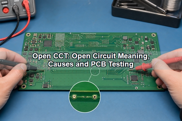
Open cct is a shortened way of writing open circuit: an electrical path is interrupted, so the affected branch cannot carry normal current. The interruption may be intentional, such as an open switch, or it may be a fault caused by a broken trace, failed via, poor solder joint, damaged connector or disconnected wire. Correct diagnosis requires checking the circuit state, measuring at the right reference points and separating a true open from a high-resistance or intermittent connection.
What Does Open CCT Mean?
In service manuals, test reports and diagnostic displays, CCT commonly abbreviates circuit. An open cct therefore means that one or more conductors in the intended path are no longer electrically continuous. The break can be complete, where current is effectively zero, or unstable, where vibration, temperature or mechanical pressure makes the connection alternate between open and conductive states.
An open circuit is a condition, not a single component. A switch in the OFF position creates an intended open. A blown fuse also opens a path, but it does so as a protection response. A cracked copper trace, unplated via or non-wetted solder joint creates an unintended open that must be located and corrected.
How Does an Open Circuit Affect Current, Voltage and Resistance?
In the ideal model, an open circuit has infinite resistance and carries zero current. Real assemblies are not ideal: a digital multimeter has finite input impedance, contaminated surfaces can leak current, and parasitic capacitance can pass a brief transient. These effects usually remain far below the current required for normal operation, but they explain why a sensitive meter may show a voltage even when the conductive path is broken.
Voltage depends on where it is measured. If a powered series circuit opens, nearly the full source voltage may appear across the break while current stays near zero. On either side of the break, voltage-to-ground readings depend on the surrounding components, pull-up or pull-down resistors, loads and measurement reference. A voltage reading alone therefore does not prove continuity.
| Quantity | Ideal open circuit | Practical interpretation |
|---|---|---|
| Current through the broken path | 0 A | Only leakage, capacitive transients or instrument current may remain |
| Resistance across the break | Infinite | A meter often displays OL or an out-of-range value |
| Voltage across the break | Can approach source voltage | Depends on the circuit topology and where the probes are referenced |
| Power delivered to the load | 0 W | The load cannot operate normally because sustained current is absent |
What Does an Open Circuit Diagram Show?
A schematic normally shows an open circuit as a visible gap, an open switch symbol or a disconnected terminal. The drawing identifies the intended electrical relationship; it does not necessarily reveal the physical location of an accidental break. A schematic may show one continuous net even when the fabricated board contains a cracked trace or an open via.
For troubleshooting, follow the net from source to load and divide it into testable sections. Mark connectors, switches, fuses, series components, vias and layer transitions because each creates a useful boundary. Comparing the schematic with board-view, netlist and layout data prevents a technician from mistaking separate nets, test points or isolated copper pours for a defect.
When Is an Open Circuit Intentional?
Open states are deliberately used wherever a design must interrupt current or isolate a signal. An open switch disables a load, a relay contact separates circuits, a transistor in cutoff approximates an open, and a high-impedance input minimizes loading. Test fixtures may also leave optional nodes unconnected by design.
- User control: an OFF switch or released normally-open pushbutton breaks the path.
- Protection: a fuse opens after excessive current, isolating the failed branch.
- Signal selection: relays, analog switches and transistor stages disconnect unused routes.
- Configuration: unpopulated jumpers or option resistors can leave a net intentionally open.
- Isolation during test: connectors or removable links separate circuits for measurement.
The design documentation should make intentional opens unambiguous. Mark no-connect pins, normally-open contacts, optional components and depopulated variants so that AOI programming, electrical test and repair instructions do not classify a correct open state as a defect.
What Causes an Open CCT on a PCB?
An unintended open cct can originate in the bare board, component, solder connection, cable or connector. The first diagnostic task is to establish whether the failure is permanent or intermittent and whether it affects one net, multiple nets or an entire power domain. A single silent input suggests a local path; several dead functions may point to a shared connector, fuse, regulator feed or return path.
Mechanical stress and temperature changes are common triggers for intermittent opens. Board flexing can separate a cracked trace, thermal expansion can move a marginal solder joint, and connector movement can disturb a worn contact. Record the failure conditions before probing because pressing on the board or moving a cable may temporarily restore the connection and hide the original evidence.
Which PCB Fabrication Defects Cause Open Circuits?
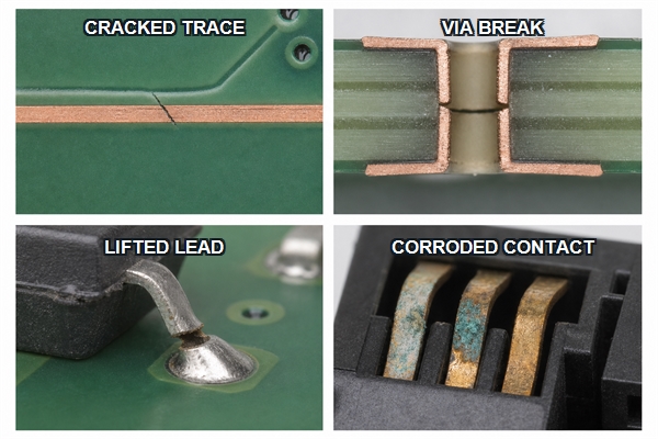
Bare-board opens occur when the copper path, plated hole or interlayer connection does not meet the netlist. Fine traces are vulnerable to over-etching, scratches and local neck-down. Vias can open because of plating voids, insufficient copper, barrel cracking or loss of connection at the capture pad. Inner-layer registration errors and drill breakout can reduce the annular connection until it fails electrical test or later separates under stress.
Reliable FR4 PCB manufacturing controls imaging, etching, drilling, desmear, copper plating and final electrical test as one connected process. The inspection plan should match the board architecture: a simple two-layer board may be fully accessible to a fixture, while fine-pitch multilayer designs often require flying-probe access, controlled test coupons and cross-section verification for critical plated structures.
- Over-etched or scratched copper traces
- Under-plated, voided or cracked via barrels
- Inner-layer pad breakout or poor layer registration
- Incomplete connection to plated-through holes
- Mechanical routing, scoring or depaneling damage
- Contamination or corrosion that progressively removes conductive material
Which Assembly Defects Cause Open Circuits?
Assembly opens usually occur at the component-to-pad interface. Insufficient solder paste, blocked stencil apertures, poor wetting, oxidized terminations, lifted leads and incorrect reflow profiles can prevent a sound joint. A tombstoned chip component leaves one terminal disconnected. BGA and QFN packages can contain hidden opens that are not visible from the top of the board.
Paste-deposit control begins with an appropriate SMT stencil, aperture design and printing process. After placement and reflow, a complete PCB assembly inspection strategy can combine solder-paste inspection, AOI, X-ray and functional testing according to package type and fault coverage. None of these methods should be treated as universal: AOI can see many exposed joints, while X-ray is more useful for hidden structures and functional test verifies behavior through an exercised path.
What Are Common Open Circuit Examples?
A lamp connected through an open switch is the simplest example: source voltage exists, but the switch gap prevents current through the lamp. On a PCB, the same electrical condition can be less obvious because the break may be microscopic or buried inside a via, package or connector.
| Example | Open location | Likely observation |
|---|---|---|
| Blown fuse | Fuse element | Downstream rail is absent; voltage may appear across the fuse |
| Cracked PCB trace | Copper conductor | One net loses continuity, sometimes only during flexing |
| Lifted IC lead | Lead-to-pad joint | A related input or output is inactive despite correct component placement |
| Open connector contact | Mating interface or crimp | Failure changes when the cable or connector is moved |
| Broken sensor wire | Harness conductor | Controller may report an open-circuit or out-of-range diagnostic code |
| Open via | Plated barrel or internal pad connection | Surface trace appears intact, but the net fails between layers |
How Can You Find an Open Circuit With a Multimeter?
De-energize the board before using resistance or continuity mode. Disconnect external power, remove batteries when practical and discharge stored energy. Measuring resistance on a live circuit can damage the meter, the board or both. Also account for capacitors, inductors and parallel paths, which can make the reading change or create an alternate route around the suspected break.
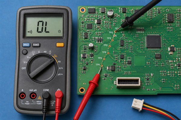
- Use the schematic and layout to identify both endpoints of the target net.
- Confirm the meter and leads by touching the probes together; continuity should sound and resistance should be near the lead resistance.
- Probe the net endpoints. OL or no beep suggests an open, but component isolation may be required.
- Divide the path at accessible pads, vias, connector pins and component terminals.
- Retest progressively smaller sections until one segment changes from conductive to open.
- Inspect that segment under magnification and use controlled flexing or thermal stimulation only when investigating an intermittent fault.
In-circuit continuity readings can be misleading because resistors, semiconductor junctions, transformers and protection devices may create alternate paths. When the result conflicts with the schematic, disconnect one component terminal or isolate the branch. The detailed multimeter testing guide explains probe placement and mode selection for broader PCB checks.
What Should a Multimeter Read Across an Open Circuit?
In resistance or continuity mode on an unpowered and isolated path, a complete open normally produces OL, O.L, infinity or a value above the selected range. The exact display depends on the meter. OL can also mean that the probes are disconnected, the range is too low for the measured resistance or the selected mode is wrong, so first verify the instrument by shorting the probes.
In voltage mode on a powered circuit, the meter may show nearly the full supply across the open because the meter itself draws very little current. For example, one probe on the source side and one on the load side of a broken series path can reveal the voltage drop at the break. Use voltage-to-ground measurements on each side to understand which node remains connected to the source and which is held by the load or another network.
What Is Open Circuit Voltage?
Open circuit voltage, commonly written VOC, is the voltage measured at a source or network output when no external load current is drawn. A high-impedance voltmeter approximates this condition. Batteries, solar cells, power supplies and sensor outputs can all have a measurable VOC.
VOC is not necessarily the voltage available under load. Internal resistance, current limiting, weak connections and source chemistry can cause the terminal voltage to fall when current is drawn. A battery may therefore show a plausible open-circuit voltage yet fail to power the circuit. Measure both unloaded and appropriately loaded behavior when source condition is in doubt.
What Is the Difference Between an Open Circuit and a Closed Circuit?
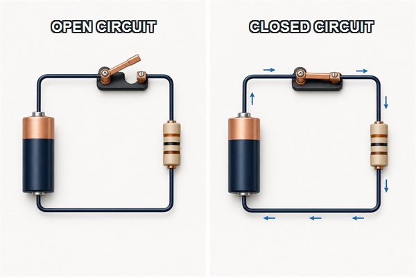
A closed circuit provides a continuous path through which current can flow when a voltage source is present. An open circuit interrupts that path. The distinction describes connectivity, not whether a design is operating correctly: a correctly opened switch and a correctly closed relay can both represent normal states.
| Condition | Path continuity | Ideal current | Typical use or symptom |
|---|---|---|---|
| Open circuit | Interrupted | 0 A | OFF switch, isolation or broken connection |
| Closed circuit | Continuous | Set by source and load | Enabled branch or completed signal path |
What Is the Difference Between an Open Circuit and a Short Circuit?
An open circuit has excessively high resistance in a path that should conduct. A short circuit has an unintended low-resistance connection between nodes that should remain separate. The resulting symptoms and risks differ sharply: an open stops the intended current, while a short can create excessive current, disturb signal levels or damage components.
| Fault | Electrical condition | Common PCB causes | Primary test |
|---|---|---|---|
| Open circuit | Required path is discontinuous | Broken trace, open via, lifted lead, poor joint | Continuity and segmented voltage tracing |
| Short circuit | Unwanted low-resistance path exists | Solder bridge, copper bridge, debris, failed component | Resistance-to-rail checks, current-limited power and thermal localization |
Do not apply unrestricted power to a board suspected of having a short. Begin with unpowered resistance checks and use a current-limited supply only within the assembly’s safe limits. For an open, voltage tracing can be useful after unpowered continuity checks establish that energizing the board is safe.
How Do PCB Factories Detect Open Circuits?
Bare-board electrical test compares actual continuity and isolation against the manufacturing netlist. Flying-probe systems are flexible for prototypes and varied builds, while fixture-based universal electrical test is efficient when volume and design stability justify dedicated tooling. These tests can detect opens between accessible net points, but the test program and access strategy must cover the required nets.

Assembly inspection adds different layers of evidence. 3D SPI checks paste deposits before placement; AOI evaluates visible component and solder conditions; X-ray examines hidden joints and internal package features; functional testing confirms behavior through exercised paths. EBest Circuit (Best Technology) can combine flying-probe or universal bare-board electrical testing with 3D SPI, AOI, X-ray and functional testing according to net access, package type and assembly structure.
These methods are complementary. AOI cannot prove the electrical continuity of every buried connection, and a basic functional test may not activate every unused interface. Test coverage should therefore be mapped to the design’s critical nets and known failure mechanisms. The related PCB circuit opening guide provides a fabrication-focused discussion of hidden and intermittent defects.
How Can Open Circuit Defects Be Prevented?
Prevention starts by removing fragile geometries and uncontrolled interfaces. Maintain practical trace widths, annular rings and copper clearances for the selected fabrication class. Add teardrops or local reinforcement where justified, protect copper from panel stress, and keep mechanically loaded connectors away from unsupported board edges. Use appropriate strain relief for cables and ensure enclosure loads do not flex solder joints.
- Follow validated trace, via and annular-ring rules instead of relying on minimum values everywhere.
- Use netlist-based bare-board electrical test for production panels.
- Design stencil apertures and reflow profiles around actual package terminations.
- Provide accessible test points on critical rails, returns, buses and safety-related signals.
- Support heavy connectors, switches and cables mechanically.
- Control moisture, ionic contamination and corrosive exposure.
- Use thermal cycling, vibration or flex testing when the service environment can drive intermittent opens.
For recurring failures, preserve the defective sample and identify the exact physical mechanism before changing multiple variables. A trace crack requires a different corrective action from a plating void, non-wetted lead or fretting connector. Process changes should be verified with the inspection method most capable of detecting that specific mechanism.
FAQ About Open CCT
Is an Open CCT Always Caused by a Broken Wire?
No. The open may be an intentional switch state or a fault in a fuse, PCB trace, via, solder joint, connector, component lead or internal component connection. The schematic and segmented continuity test identify which portion of the path is open.
Can an Open Circuit Be Intermittent?
Yes. Cracked solder joints, fatigued traces, damaged vias and worn connector contacts can change resistance with vibration, board flex or temperature. Logging the failure condition and testing under controlled stress can reveal a fault that disappears at room temperature on a stationary bench.
What Does Open CCT Mean in an Automotive Diagnostic Code?
It generally means the control module detects a missing electrical path or an out-of-range voltage consistent with an open circuit. The cause may be a broken harness conductor, disconnected plug, corroded terminal, failed load, poor ground or internal module fault. The exact test sequence must follow the vehicle wiring diagram and code definition.
Can a Board Pass Visual Inspection and Still Contain an Open Circuit?
Yes. A buried via crack, internal layer separation, hidden package joint or microscopic trace break may not be visible. Netlist electrical testing, X-ray, functional testing or sectional analysis may be required, depending on the suspected location.
Conclusion
Open cct means that an intended current path is interrupted. The most reliable diagnosis combines the schematic, safe continuity testing, voltage measurements at defined references and progressive isolation of the failed segment. In PCB production, netlist electrical test, paste inspection, AOI, X-ray and functional testing each address different open-circuit risks.
For PCB fabrication or PCBA support with test coverage matched to your board structure, contact EBest Circuit (Best Technology) at sales@bestpcbs.com.
You may also like







Tags: multimeter, open cct, open circuit, open circuit meaning, open circuit test, PCB Assembly, PCB testing