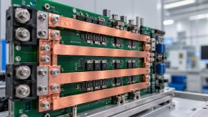
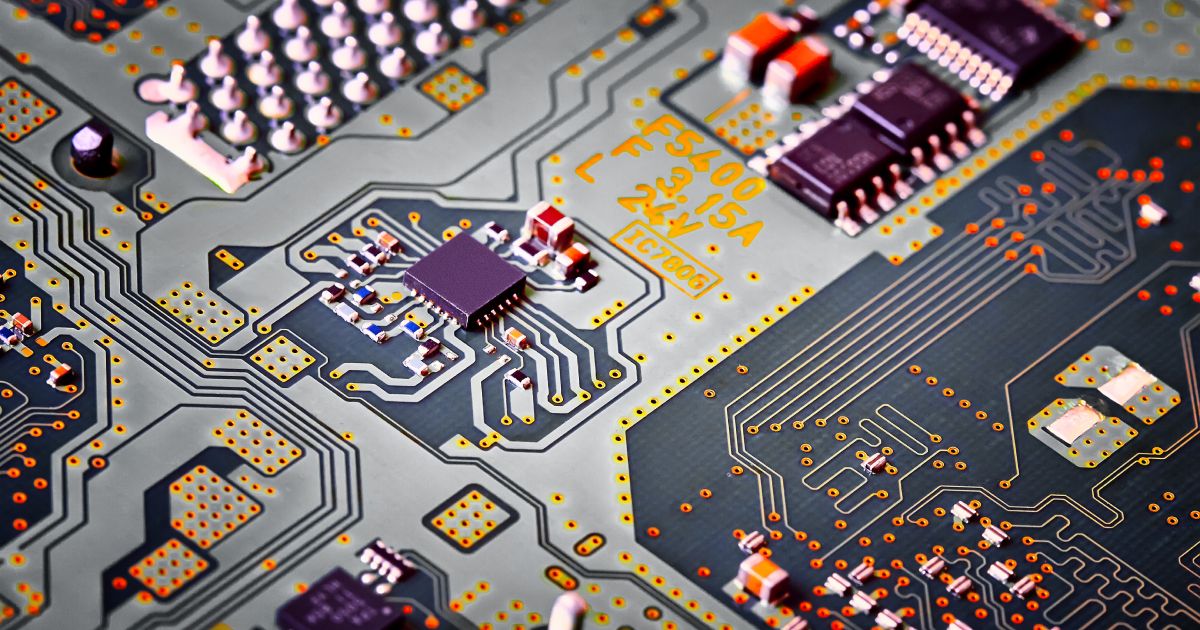
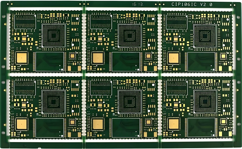
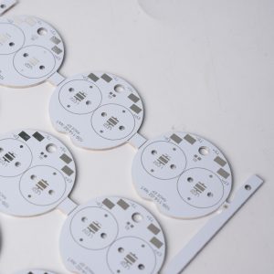
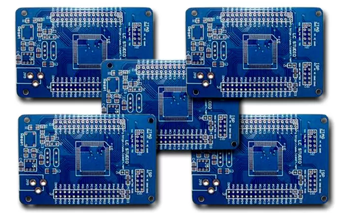
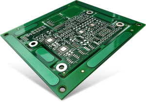
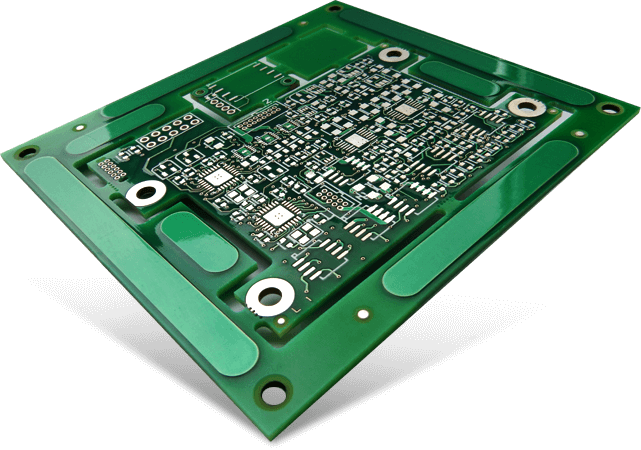
Copper pad design plays a direct role in PCB solderability, current flow, mechanical bonding, test access, and long-term circuit reliability. On a circuit board, these exposed copper areas may look simple, but they carry several important functions. They connect components, support solder joints, provide test points, and help create stable electrical interfaces.
This guide explains what a copper pad is, how it differs from a solder pad or copper contact pad, how pads are made during PCB fabrication, what surface finishes are used, and how damaged pads can be handled during prototyping or board evaluation.
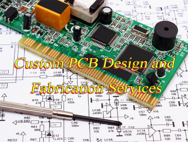
If your project involves fine-pitch components, high-current pads, contact pads, or repeated soldering concerns, an early DFM review can help identify risks before fabrication and assembly. Best Technology provides PCB manufacturing, PCBA assembly, surface finish guidance, and engineering support for prototype and production projects. For a technical review or quotation, pls feel free to send your Gerber files and BOM to sales@bestpcbs.com.
What Is a Copper Pad on a PCB?
A copper pad on a PCB is a defined copper area used for electrical connection, component attachment, testing, or signal transfer. It is created from the copper layer of the circuit board and exposed through the solder mask so that solder, probes, connectors, or conductive surfaces can make contact with it.
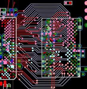
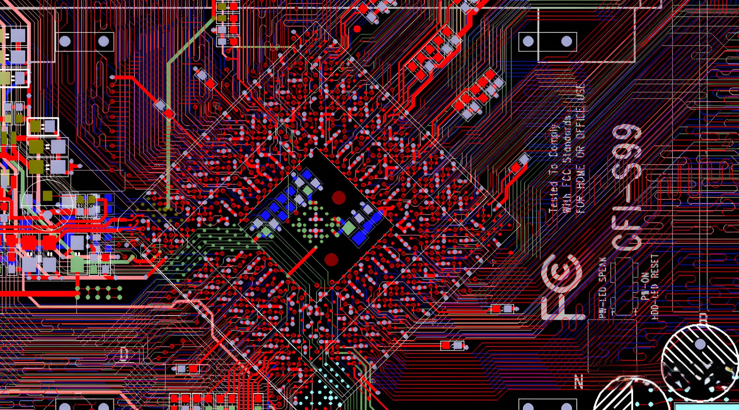
In PCB manufacturing, copper pads are formed together with copper traces, planes, vias, and other conductive features. During fabrication, unwanted copper is removed through imaging and etching, leaving the designed circuit pattern on the board. After that, solder mask is applied, and selected pad areas remain open for assembly or contact.
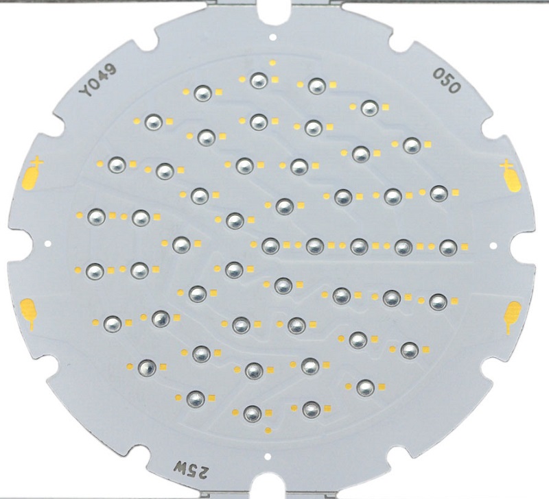
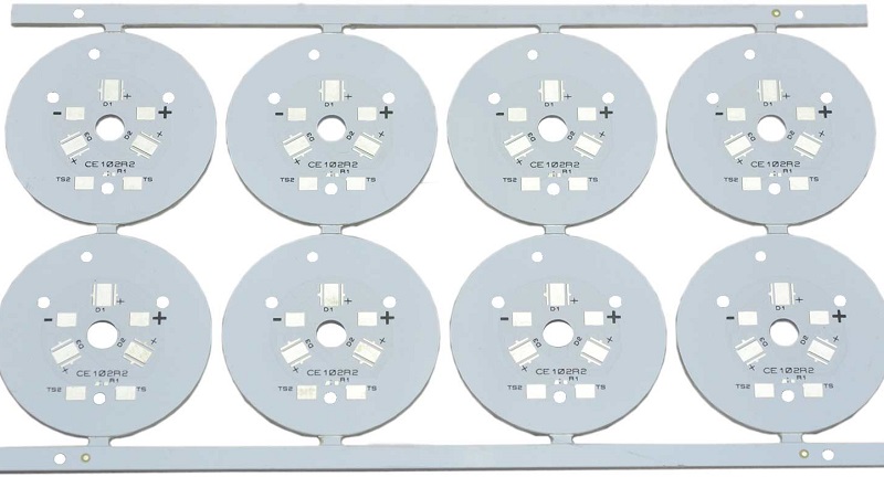
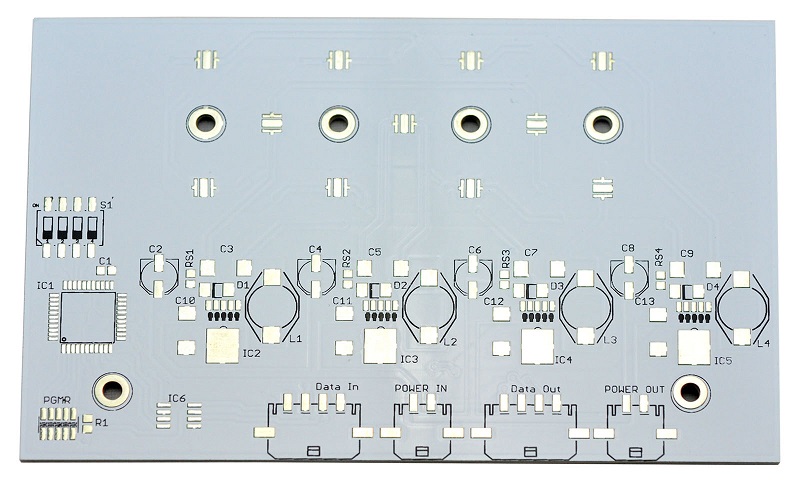
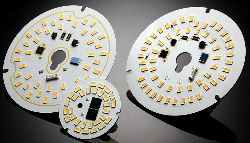
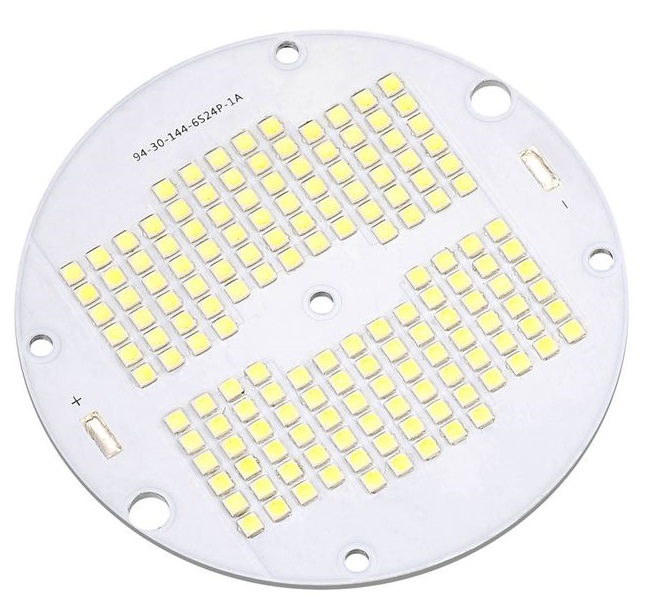
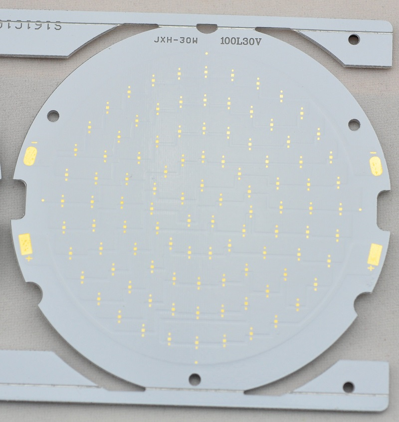
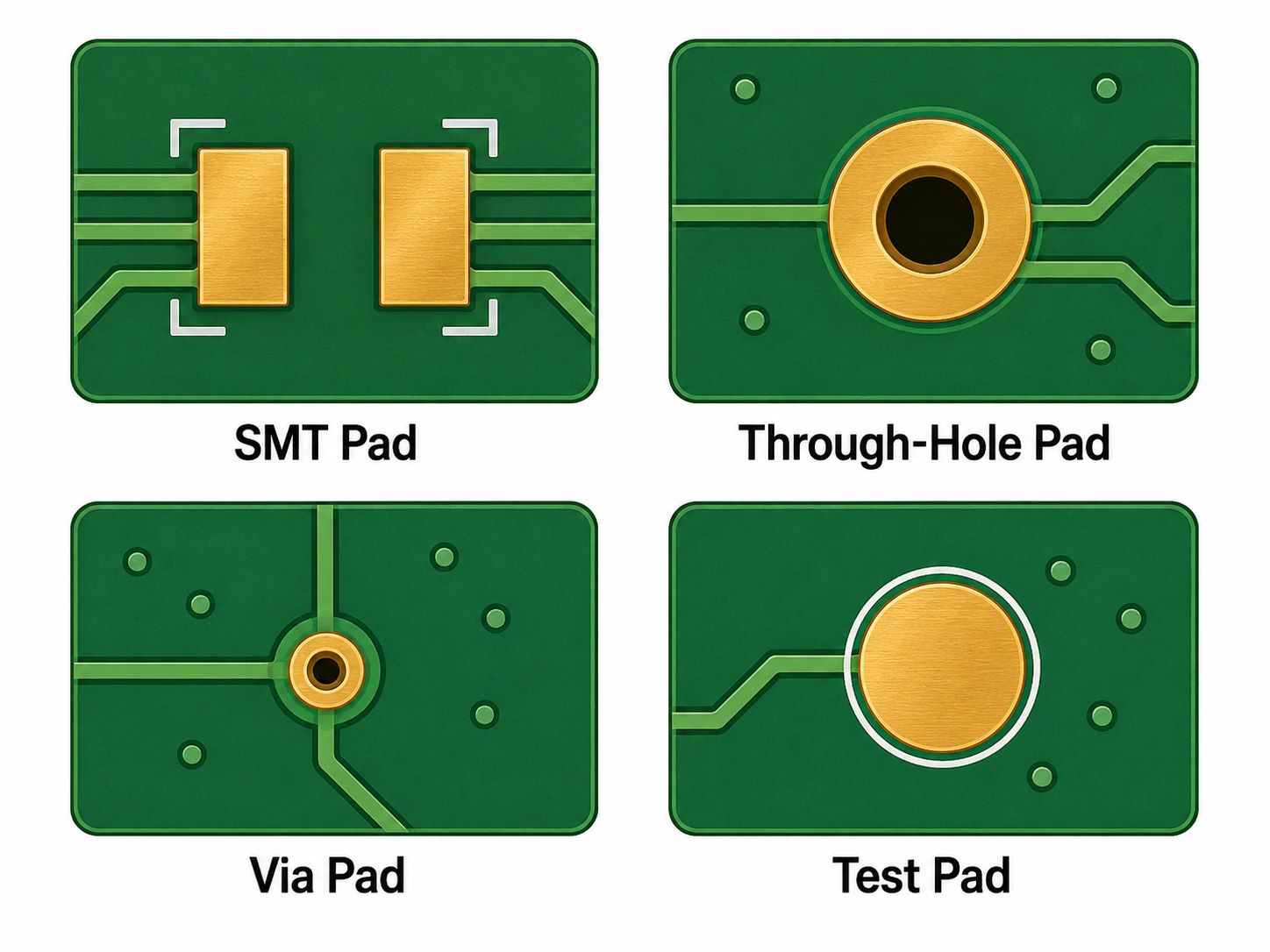
A PCB may contain many types of pads, including:
- SMT pads for surface mount components
- Through-hole pads for leaded components
- Via pads for interlayer connection
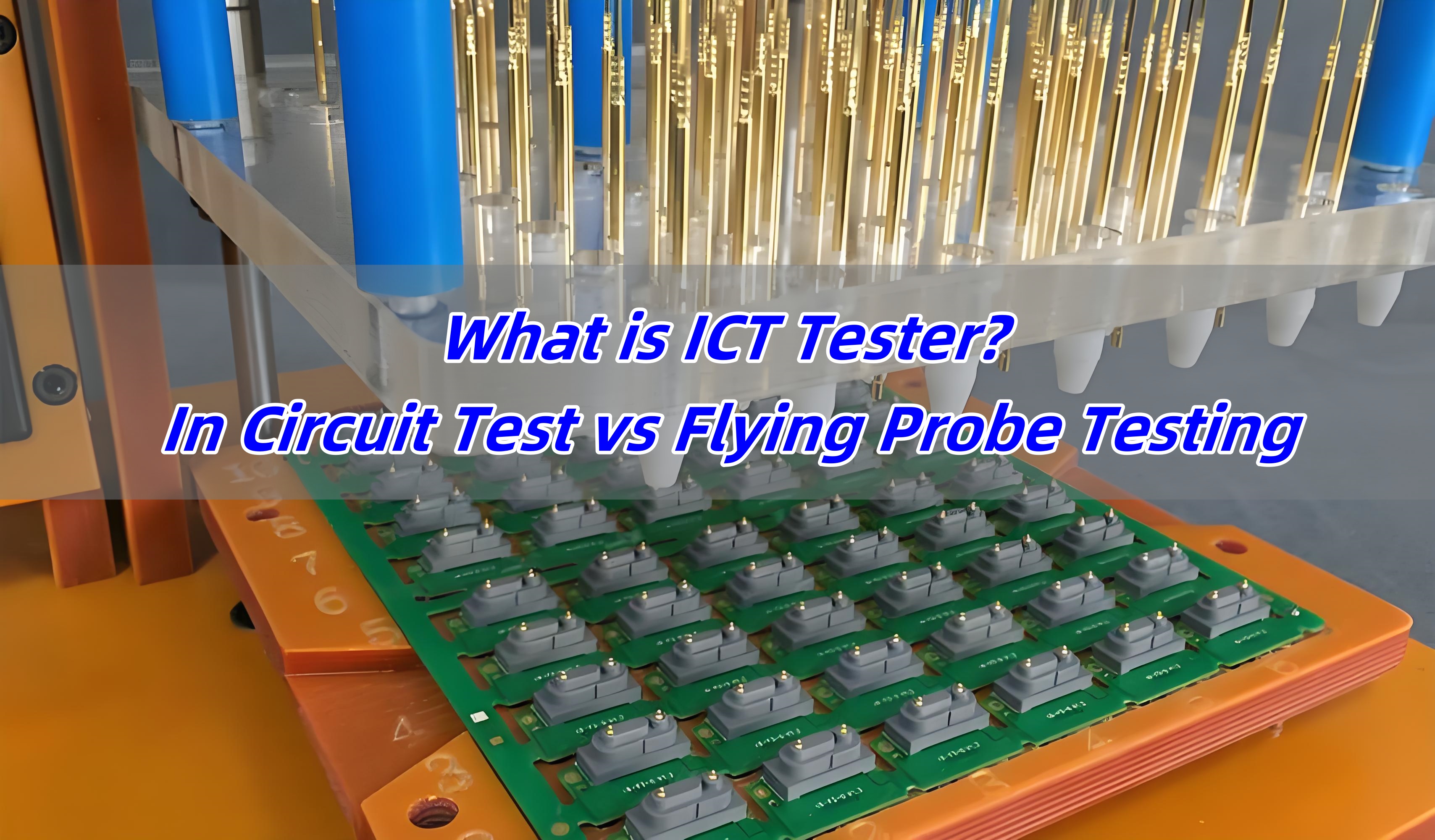
- Test pads for ICT or functional testing
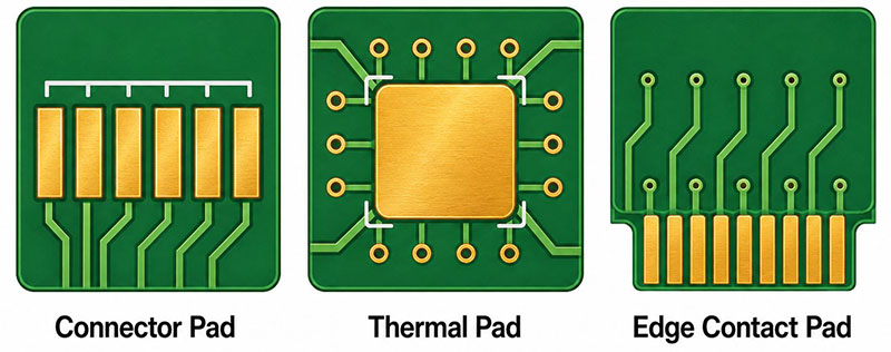
- Connector pads for board-to-board or cable interfaces
- Thermal pads for heat transfer under power components
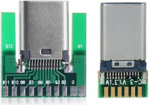
- Edge contact pads for card-edge connectors
Each pad type has its own design requirements. An 0402 resistor pad, for example, is very different from a high-current terminal pad or a BGA pad. The layout engineer must consider component footprint, assembly process, current capacity, plating finish, and inspection method before finalizing the pad design.
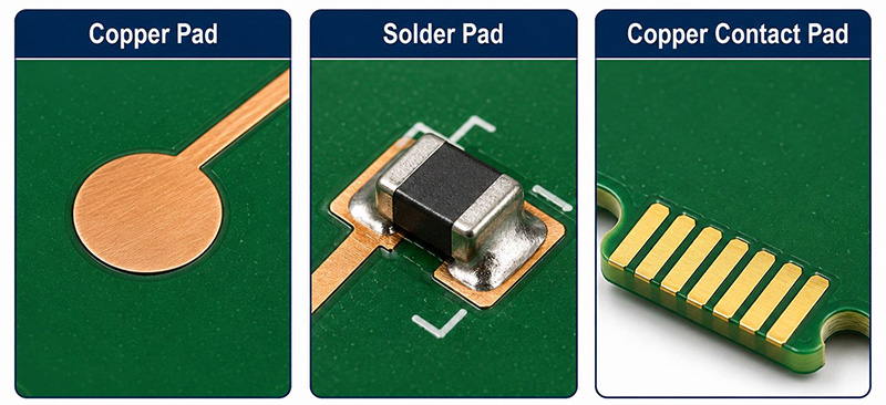
What Is the Difference Between a Copper Pad, Solder Pad, and Copper Contact Pad?
These terms are sometimes used interchangeably, but they are not exactly the same. Understanding the difference helps engineers communicate clearly with PCB manufacturers and assembly teams.
| Term | Meaning | Common Use |
|---|---|---|
| Copper pad | A copper area designed on the PCB layout | General term for exposed or plated copper features |
| Solder pad | A pad designed to receive solder and attach a component | SMT and through-hole component assembly |
| Copper contact pad | A conductive contact area for mechanical or electrical contact | Connectors, switches, test probes, battery contacts |
| Test pad | A pad used for electrical testing | ICT, flying probe, functional test |
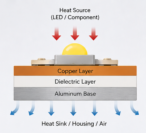
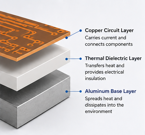
| Thermal pad | A pad used for heat transfer and sometimes grounding | Power ICs, LEDs, MOSFETs, thermal vias |
A solder pad is usually a copper pad with a surface finish applied, such as ENIG, HASL, OSP, immersion silver, or immersion tin. Its main purpose is to form a reliable solder joint between the PCB and the component terminal.
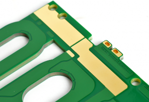
A copper contact pad may not always be intended for soldering. It may be used for spring contacts, pogo pins, keypads, battery terminals, or edge connectors. In these applications, wear resistance, flatness, plating hardness, and oxidation control become very important.
For example, a gold-plated edge connector pad is a copper contact pad. It needs strong abrasion resistance because it may be inserted and removed many times. A standard SMT capacitor pad has a different requirement: it needs good solder wetting and accurate solder paste deposition.
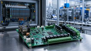
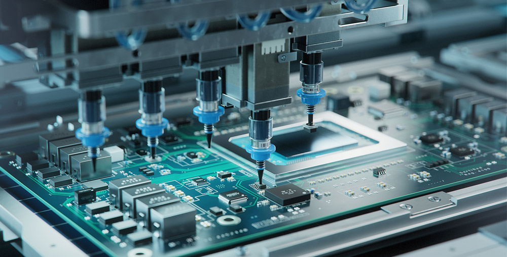
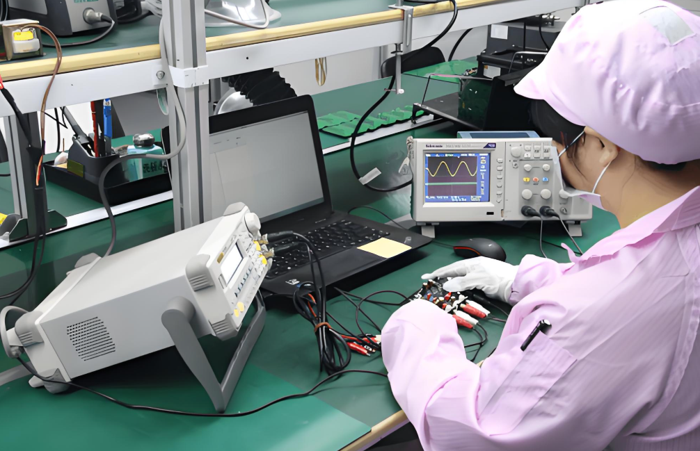
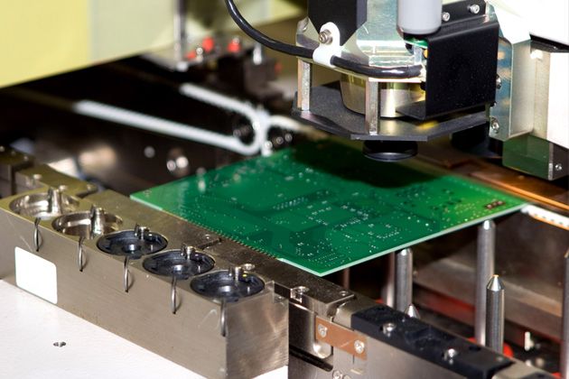
What Does a Copper Pad Do in PCB Assembly?
During PCB assembly, pads provide the interface between the bare circuit board and electronic components. The solder paste is printed onto the pads, components are placed on top, and the assembly is heated during reflow soldering. When solder melts and wets the pad surface, it creates both mechanical attachment and electrical continuity.
A properly designed pad supports several assembly goals.
It helps solder wet evenly.
- Good solder wetting depends on a clean surface, suitable finish, correct pad geometry, and proper reflow profile. When these factors are controlled, solder spreads across the pad and forms a stable joint.
It keeps components in position.
- Pad symmetry matters. If one pad is much larger than the other, or if thermal connection is uneven, small components may shift during reflow. This can lead to tombstoning, skewing, or weak solder joints.
It supports electrical performance.
- The pad connects the component terminal to traces, vias, planes, or other copper features. For high-speed, RF, or high-current boards, pad geometry can affect impedance, parasitic capacitance, current distribution, and heat spreading.
It improves inspection access.
- Pads must allow AOI, X-ray, probe testing, or visual inspection depending on the board type. For BGA packages, hidden solder joints may require X-ray inspection. For test points, pad size and spacing must match fixture or flying probe capability.
It contributes to mechanical reliability.
- A pad must stay bonded to the PCB substrate through soldering, handling, thermal cycling, and product operation. Copper adhesion, laminate quality, surface treatment, and assembly temperature all influence pad strength.
In short, pad design connects PCB fabrication with PCBA reliability. A small layout decision can affect paste printing, placement accuracy, solder joint quality, test coverage, and field performance.
Copper Pad PCB Design: Size, Shape, Clearance, and Annular Ring
A strong PCB pad design starts with the component datasheet and IPC footprint guidance. The pad must match the component lead, terminal, or ball while also fitting the assembly process used by the manufacturer.
Pad Size
Pad size affects solder volume, wetting area, and joint strength. If the pad is too small, solder coverage may be insufficient. If it is too large, solder may spread too far and create floating, skewing, or bridging risks. For fine-pitch ICs, even a slight size deviation can affect assembly yield.
For SMT components, pad size is usually determined by:
- Component terminal dimensions
- Solder fillet requirement
- Placement tolerance
- Solder paste stencil design
- Assembly process capability
- Product reliability class
Pad Shape
Common pad shapes include rectangular, round, oval, square, and custom thermal shapes. Rectangular pads are common for chip resistors, capacitors, IC leads, and connectors. Round or oval pads are often used for through-hole parts and vias.
For RF or high-frequency boards, pad shape may also influence signal transition. In these cases, pad design should be reviewed together with impedance control, reference plane continuity, and via structure.
Clearance
Clearance is the spacing between a pad and nearby copper features. It affects manufacturability, voltage isolation, solder mask definition, and assembly quality. High-voltage circuits need larger clearance and creepage distance. Fine-pitch designs require tighter control from the PCB manufacturer.
Designers should check clearance between:
- Pad to pad
- Pad to trace
- Pad to via
- Pad to copper pour
- Pad to board edge
- Pad to mechanical hole
Annular Ring
For plated through-hole pads and vias, the annular ring is the copper area surrounding the drilled hole. It provides a reliable connection between the plated barrel and the surface copper pad.
If the annular ring is too narrow, drilling tolerance may reduce copper support around the hole. This can affect soldering, mechanical strength, and electrical connection. For high-reliability boards, annular ring design should consider drill accuracy, finished hole size, copper plating thickness, and IPC class requirements.
Solder Mask Opening
Solder mask defines which part of the copper surface is exposed. Two common pad styles are solder mask defined and non-solder mask defined.
| Pad Style | Description | Typical Use |
|---|---|---|
| Non-solder mask defined | Solder mask opening is larger than the copper pad | Common SMT pads |
| Solder mask defined | Solder mask overlaps the copper pad edge | Some BGA and fine-pitch applications |
Non-solder mask defined pads are widely used because the copper edge defines the solderable area. Solder mask defined pads can help control pad exposure in certain dense designs, but they require precise solder mask registration.
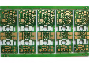
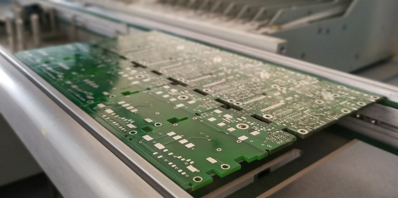
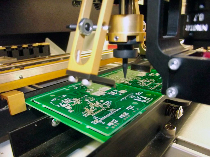
How Are Copper Pads Cut, Etched, and Plated on a PCB?
Copper pads are not usually “cut” one by one. They are formed during the PCB imaging and etching process. The manufacturer starts with copper-clad laminate or copper foil laminated onto the PCB core. The desired circuit pattern is transferred onto the copper surface using photoresist and imaging.
The general process includes:
- Copper-clad material preparation
The PCB base material is prepared with copper foil on one or both sides, depending on the stack-up. - Cleaning and surface preparation
The copper surface is cleaned to improve photoresist adhesion and imaging accuracy. - Photoresist application
A photosensitive film is applied to the copper surface. - Circuit imaging
The pad, trace, and plane pattern is exposed using the PCB artwork data. - Developing
Unwanted photoresist is removed, leaving protected copper areas according to the circuit design. - Etching
Exposed copper is chemically removed. The remaining copper forms pads, traces, and other conductive features. - Drilling and plating
For plated holes and vias, drilling is followed by copper deposition and electroplating to create conductive barrels. - Solder mask application
Solder mask covers most copper areas while leaving pads exposed. - Surface finish
A protective finish is applied to exposed pads to improve solderability and prevent oxidation.
For multilayer PCBs, copper pads may exist on outer layers, inner layers, or both. Inner-layer pads connect to vias or buried structures, while outer-layer pads are often used for assembly and testing.
Etching accuracy matters because copper width, pad size, and spacing must remain within manufacturing tolerance. The final pad geometry depends on copper thickness, etching compensation, imaging accuracy, and process control.
What Surface Finishes Are Used on Copper Pads?
Bare copper oxidizes when exposed to air. Oxidation can reduce solderability and create unreliable contact surfaces. For this reason, exposed pads are protected with a surface finish after solder mask processing.
The surface finish should match the assembly method, component type, shelf-life requirement, cost target, and reliability expectation.
| Surface Finish | Main Features | Common Applications |
|---|---|---|
| HASL | Good solderability, cost-effective, uneven surface | General electronics, larger components |
| Lead-Free HASL | RoHS-compatible version of HASL | Standard lead-free assembly |
| ENIG | Flat surface, good solderability, nickel-gold structure | Fine-pitch ICs, BGA, high-reliability PCB |
| OSP | Organic coating, flat and economical | SMT boards with controlled storage and fast assembly |
| Immersion Silver | Flat finish, good conductivity | High-speed, RF, and lead-free assembly |
| Immersion Tin | Flat surface, good solderability | Press-fit, fine-pitch, and selected lead-free applications |
| Hard Gold | Excellent wear resistance | Edge connectors, keypads, contact pads |
- ENIG is widely used for fine-pitch components because it provides a flat soldering surface. The nickel layer acts as a diffusion barrier, and the thin gold layer protects the nickel before soldering.
- OSP is common for cost-sensitive SMT production. It protects copper pads before assembly but requires good storage control and proper handling.
- Hard gold is preferred for copper contact pad applications where repeated mechanical contact is expected. It is not the same as soft immersion gold used in ENIG. Hard gold is thicker and more wear-resistant.
- HASL provides strong solderability but may create an uneven surface. For very fine-pitch components, BGA, or small passive components, flatter finishes are usually preferred.
Choosing the right finish helps improve solder joint consistency, test contact stability, and long-term product reliability.
How to Fix a Copper Pad on a Circuit Board?
A lifted or missing pad can happen during prototype debugging, excessive rework, overheating, mechanical stress, or poor handling. In lab repair, technicians may use micro-jumpers, conductive epoxy, replacement pad kits, or copper foil methods to restore electrical connection. However, for production boards, pad damage should be treated as a process or design issue, not a normal repair step.
Common causes of pad damage include:
- Excessive soldering iron temperature
- Long dwell time during manual rework
- Poor copper adhesion to the laminate
- Repeated component removal
- Strong mechanical pulling force
- Incorrect footprint design
- Insufficient annular ring on through-hole pads
- Incompatible reflow or rework profile
For prototypes, a technician may repair a damaged pad by reconnecting the component terminal to the correct trace or via. If the original pad is connected to a nearby trace, a fine wire jumper may be used. If it connects to a via or inner layer, the repair becomes more difficult and requires careful electrical verification.
Copper tape is sometimes used as a temporary repair material. It may help recreate a missing solderable area in low-risk prototypes, but it is not a preferred solution for production electronics. Adhesion strength, solderability, current capacity, and long-term stability must be checked carefully.
For manufacturing improvement, the better approach is to review:
- Pad size and copper area
- Laminate selection
- Copper peel strength
- Soldering temperature profile
- Rework method
- Component footprint
- Operator handling process
- Board storage and moisture control
If pad lifting appears repeatedly, the board design and assembly process should be reviewed together. A DFM check can identify pad geometry issues, thermal imbalance, solder mask problems, and potential assembly risks before mass production.
For PCB projects requiring stable pad quality, Best Technology can support PCB fabrication, surface finish selection, DFM review, PCBA assembly, and testing. For project discussion or quotation, contact sales@bestpcbs.com.
FAQs About Copper Pad
1. What is a copper pad on a PCB?
A copper pad is a defined copper area on a circuit board used for soldering, electrical contact, testing, or connection. It can support SMT components, through-hole leads, probes, connectors, or thermal transfer structures.
2. Is a copper pad the same as a solder pad?
Not always. A solder pad is a type of copper pad designed for soldering components. A copper pad can also be used as a contact pad, test pad, via pad, or thermal pad.
3. What is a copper contact pad used for?
A copper contact pad is used for direct electrical contact. Common examples include edge connectors, spring contacts, pogo pin test points, keypad contacts, and battery terminals. These pads often need a durable surface finish such as hard gold.
4. How are copper pads made on a PCB?
Copper pads are formed through PCB imaging and etching. The manufacturer protects the required copper pattern and removes unwanted copper. After solder mask processing, exposed pads receive a surface finish such as ENIG, HASL, OSP, immersion silver, or hard gold.
5. Why do copper pads need surface finish?
Bare copper can oxidize. A surface finish protects the pad, improves solderability, and supports reliable electrical contact. The finish is selected based on assembly process, component pitch, storage condition, and product reliability requirements.
6. Can you replace a missing solder pad with copper tape?
Copper tape may be used as a temporary prototype repair in some simple cases. It should be verified for adhesion, electrical continuity, solderability, and current capacity. For production boards, redesign, controlled rework, or professional process review is a better solution.
7. Why does a copper pad lift from a PCB?
Pad lifting can be caused by excessive heat, repeated rework, mechanical force, weak copper adhesion, poor footprint design, or unsuitable soldering conditions. Reviewing the pad design and assembly profile helps prevent repeated failures.
8. Which surface finish is best for copper pads?
There is no single best finish for every PCB. ENIG is suitable for fine-pitch and BGA assembly, OSP is economical for controlled SMT production, HASL works well for many general boards, and hard gold is suitable for contact pads that require wear resistance.
Have a PCB or PCBA project that requires reliable copper pad design? Best Technology supports rigid PCB, multilayer PCB, HDI PCB, flexible PCB, rigid-flex PCB, heavy copper PCB, aluminum PCB, copper substrate PCB, ceramic PCB, and Rogers/high-frequency PCB manufacturing, together with DFM review, surface finish guidance, component sourcing, PCBA assembly, and testing.
If you would like our engineering team to help review pad size, solder mask opening, annular ring, copper thickness, surface finish, or soldering reliability before production, please feel free to send your Gerber files and BOM to sales@bestpcbs.com. We would be glad to provide a technical review or quotation based on your project needs.