





Automated x ray inspection pcb helps buyers find hidden solder-joint risks that visual inspection or automated optical inspection cannot see beneath BGA, QFN, LGA, and other bottom-terminated packages.
However, simply requesting “X-ray inspection” does not define the inspection coverage, acceptance criteria, records, or response to a failed result. This guide explains what buyers should specify when automated X-ray inspection is part of a PCB assembly quality plan.
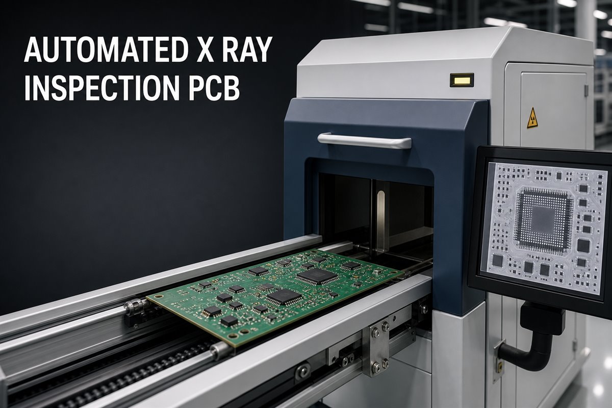
How Does Automated X Ray Inspection PCB Production Work?
An AXI system directs X-rays through an assembled circuit board and records how different materials absorb the radiation. Dense materials, including solder and copper, produce different grayscale patterns from laminate, component bodies, and air gaps.
Inspection software then evaluates selected regions against programmed criteria. Depending on the equipment and inspection plan, the system may check solder-joint shape, void area, ball alignment, bridging, missing connections, or barrel fill.
A repeatable automated sequence includes:
- Identify the board or production program.
- Align the PCB using fiducials or programmed reference points.
- Capture images of selected components and solder joints.
- Apply predefined inspection algorithms.
- Classify results as acceptable, defective, or requiring review.
- Store inspection images and result data when traceability is required.
- Route a suspected assembly for verification or rework.
Automation improves consistency and throughput, but it does not remove engineering judgment. The inspection program, image quality, component geometry, acceptance limits, and review process still determine whether the result is useful.
Before placing an order, buyers should identify the critical packages, required inspection coverage, applicable workmanship criteria, and evidence expected with the shipment.
When Should Buyers Require Automated X Ray Inspection?
Not every component on every PCBA requires X-ray inspection. Visible components may be inspected effectively with AOI, while electrical and functional tests evaluate different risks.
AXI becomes more valuable when solder joints cannot be seen directly or when a hidden defect could create expensive rework or field failure.
Common reasons to require AXI include:
- BGA, micro-BGA, CSP, LGA, or bottom-terminated components
- QFN or DFN packages with thermal pads
- Package-on-package assemblies
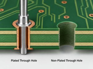
- Press-fit or through-hole connections requiring barrel-fill evaluation
- Double-sided PCB assemblies with overlapping components
- High-density boards with limited optical access
- First-article validation for a new component or assembly process
- Investigation of intermittent failures
- High-volume production requiring repeatable inspection
- Projects with customer-defined traceability requirements
The appropriate coverage may change during the product lifecycle. A prototype may need focused inspection of several critical joints. A first article may require broader evidence to validate the assembly process. Stable mass production may use risk-based sampling or an agreed automated inspection rate.
Buyers should not assume that every PCBA requires 100% AXI. The requirement should reflect component risk, production volume, process maturity, failure consequences, and the customer’s acceptance plan.
Inline X-Ray Inspection for High-Volume PCB Assembly
Inline AXI is integrated with the production flow so assemblies can enter, be inspected, and continue through the line with limited manual handling. It is most relevant when inspection speed, repeatability, and production data are important.
A high-volume product may justify inline AXI when it contains many hidden joints, requires consistent board-to-board inspection, or needs rapid feedback on assembly-process changes.
Buyers should clarify:
- Whether every board or only selected boards will be inspected
- Which components and regions are included in the program
- Whether the system performs 2D, 2.5D, or 3D analysis
- How double-sided assemblies are handled
- What happens when the machine flags a defect
- Whether a trained inspector reviews uncertain results
- How results connect to the board, panel, batch, or serial number
- Whether failed assemblies are reworked and inspected again
Inline inspection can provide faster process feedback. Repeated voiding or solder-volume variation may indicate a stencil, solder-paste, placement, or reflow issue. Finding the pattern during production can reduce the number of boards affected.
For prototypes, small batches, failure analysis, or targeted inspection, an offline or manually loaded system may provide sufficient flexibility. The buyer’s goal is to obtain inspection coverage and evidence appropriate to the project risk.
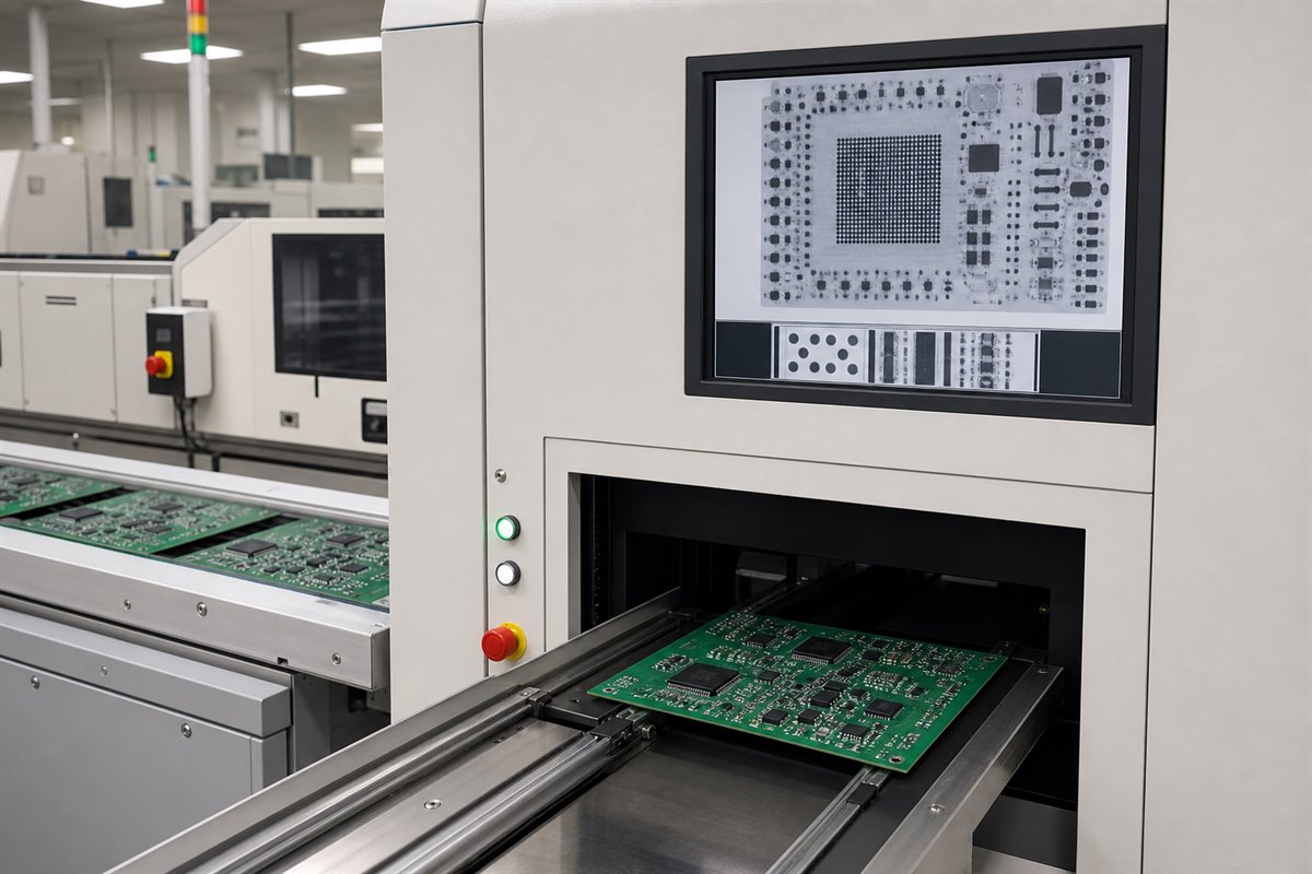
Automated X-Ray Inspection vs AOI
AXI and AOI examine different features of a PCB assembly. They complement each other and should not be treated as interchangeable.
| Inspection method | Strongest application | Typical limitations |
| AOI | Component presence, polarity, alignment, and visible solder joints | Cannot see solder joints hidden beneath component bodies |
| AXI | Hidden joints, internal solder distribution, voids, and certain through-hole conditions | May produce overlapping images or false calls and cannot verify circuit function |
| Electrical testing | Opens, shorts, and selected electrical conditions | May not identify the physical cause of a defect |
| Functional testing | Product behavior under customer-defined conditions | Passing results do not reveal every structural solder defect |
AOI can identify visible problems such as missing components, reversed polarity, tombstoning, misalignment, and abnormal exposed solder fillets. AXI is used where optical access is blocked, particularly under BGAs, QFNs, LGAs, and other bottom-terminated packages.
A strong PCB testing plan assigns each risk to the appropriate method. AOI may check placement and polarity, AXI may examine BGA joints, and functional testing may confirm behavior defined in the customer’s procedure. Requesting AXI alone does not create complete PCBA quality assurance.
2D vs 3D X-Ray Inspection
A 2D X-ray image combines structures between the source and detector into one projection. It can reveal solder bridges, missing balls, obvious voids, misalignment, and differences in solder distribution.
The challenge is overlap. Copper features, components, solder joints, and structures on the opposite side of a double-sided assembly may appear in the same image.
Three-dimensional or computed-tomography-based inspection captures images from multiple angles and reconstructs selected layers or cross-sections. This can help separate joints on opposite sides and provide more detailed information about complex packages.
| Project condition | Possible inspection approach |
| Single-sided assembly with accessible BGA patterns | 2D inspection may provide sufficient information |
| Double-sided assembly with overlapping joints | 3D analysis may separate top- and bottom-side structures |
| QFN thermal-pad void evaluation | 2D or 3D selection depends on geometry and acceptance needs |
| Complex package-on-package assembly | 3D inspection may provide clearer separation |
| Prototype troubleshooting | Flexible offline or angled inspection may be appropriate |
| High-volume production | Inspection coverage must be balanced with cycle time |
A more advanced image does not automatically produce a more reliable decision. Resolution, viewing angle, reconstruction method, program settings, component design, and operator review all influence the result.
What Can X Ray Solder Joint Inspection Detect?
X-ray inspection can reveal structural differences hidden beneath components, but detectability depends on the package, board construction, equipment, image quality, and programmed criteria.
Common findings include:
- Solder voids
- Bridging between adjacent joints
- Missing solder balls
- Insufficient solder
- Excessive solder
- Ball or component misalignment
- Inconsistent solder-joint shape
- Open or poorly formed connections
- Head-in-pillow indications
- Abnormal through-hole barrel fill
Each finding creates a different customer risk. A bridge may produce a short circuit, while an incomplete joint can cause an open or intermittent connection. Excessive voiding can reduce the effective soldered area and affect mechanical or thermal performance.
A visible void does not automatically mean the assembly must be rejected. Its location, size, distribution, component type, product requirements, and applicable acceptance criteria all matter.
The customer should define or approve:
- Critical components and joints
- Applicable workmanship standard and class
- Customer-specific acceptance criteria
- Void measurement method where required
- Sampling or inspection coverage
- Disposition of borderline results
- Required documentation
Without these inputs, the supplier may detect an image feature but still lack the authority to determine whether it is acceptable for the final product.
How Do AXI False Calls Affect Production?
A false call occurs when the automated system flags an acceptable feature as a possible defect. False calls can result from component variation, overlapping structures, image noise, unsuitable program limits, or differences between the actual board and the inspection reference.
Excessive false calls slow production, increase manual review, and may cause unnecessary rework. Limits that are too broad create the opposite risk: a real defect may not be flagged.
Important controls include:
- Using the correct PCB revision and inspection program
- Confirming component locations against released assembly data
- Establishing suitable regions of interest
- Setting limits for the actual package geometry
- Reviewing known-good and known-defective samples where available
- Tracking repeated false calls by component and defect type
- Revalidating the program after relevant design or process changes
- Requiring human review for uncertain results
Buyers should ask how the manufacturer handles a failed AXI result. An automated “NG” output should lead to a defined verification and disposition process, not immediate uncontrolled rework.
What AXI Inspection Evidence Should Buyers Request?
A verbal statement that a board “passed X-ray” may be insufficient for a critical project. Buyers should define what evidence is needed before production begins.
Useful AXI evidence may include:
- PCB or assembly identification
- Production lot, panel, or serial number
- Inspection date
- PCB revision and AXI program revision
- Inspected component references
- Inspection coverage or sampling plan
- Representative X-ray images
- Flagged defect type and location
- Pass, fail, or review result
- Approved disposition
- Rework and reinspection status
- Inspector or reviewer identification when required
The necessary record level should match the project. A routine commercial assembly may only need confirmation that the agreed inspection was completed. A high-reliability or traceability-controlled project may require component-level images and board-specific records.
Before quotation, provide Gerber files, BOM, pick-and-place data, assembly drawings, component references, inspection requirements, and acceptance criteria. This allows the manufacturer to evaluate whether the requested coverage and evidence are practical.
EBest Circuit (Best Technology) can review PCB manufacturability, support PCB fabrication and circuit board assembly, and coordinate agreed inspection and testing activities. Available X-ray method, coverage, reporting, and acceptance requirements should be confirmed for the specific project during quotation.
The customer remains responsible for the released design, product-specific acceptance criteria, regulatory requirements, and final product validation.
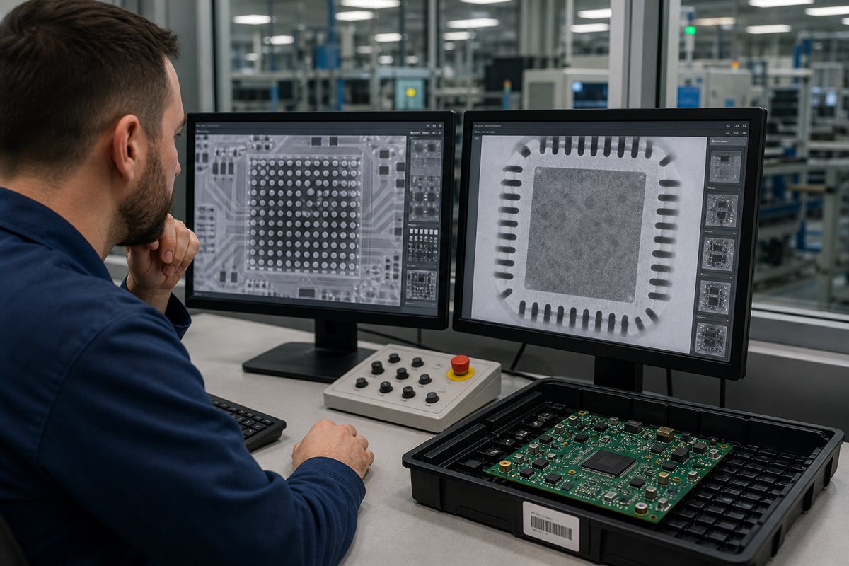
A Realistic BGA Assembly Inspection Plan
Consider a double-sided industrial-control PCBA containing a fine-pitch BGA, two QFN power devices, and several visible connectors.
The customer’s main concern is preventing hidden-joint problems from reaching system integration, where intermittent faults would be more expensive to diagnose.
- Review the released Gerber files, BOM, pick-and-place file, assembly drawing, and critical-component list.
- Confirm the BGA and QFN references requiring X-ray inspection.
- Use AOI for component presence, polarity, alignment, and visible solder conditions.
- Use the agreed X-ray method for hidden BGA and QFN joints.
- Review voiding, bridging, alignment, solder distribution, and other specified conditions.
- Record findings against the appropriate board, panel, batch, or serial number.
- Segregate assemblies with suspected defects.
- Obtain approval for any result outside the agreed criteria.
- Reinspect affected joints after authorized rework.
- Complete the customer-defined electrical or functional testing separately.
This plan separates the responsibilities of each inspection method and gives the buyer a clearer basis for comparing quotations. A quote stating only “X-ray inspection included” does not show whether one sample, every critical package, or every production board will be inspected.
FAQs About Automated X-Ray Inspection
Does every PCB assembly need automated X-ray inspection?
No. AXI is most valuable for hidden joints, complex assemblies, high production volumes, or projects in which an undetected solder defect creates significant risk.
Can AXI replace automated optical inspection?
No. AXI is strong at inspecting hidden internal structures, while AOI is efficient for visible component and solder conditions.
Does passing AXI prove that a PCBA works correctly?
No. AXI evaluates structural image features. It does not prove firmware operation, signal performance, power behavior, or complete product functionality.
Should buyers request 100% AXI inspection?
It depends on component risk, volume, process maturity, failure consequences, and traceability needs. Buyers should define critical joints and required coverage.
What files are needed to quote AXI with PCB assembly?
Provide Gerber files, BOM, pick-and-place data, assembly drawing, critical-component list, quantity, acceptance criteria, inspection coverage, and reporting requirements.
For a PCB or PCBA quotation involving hidden-joint inspection, send your project files and inspection requirements to sales@bestpcbs.com. EBest Circuit (Best Technology) can review the manufacturing package and confirm the available inspection support for the agreed production scope. Learn how automated x ray inspection pcb requirements fit your project before production begins.
You may also like


Tags: automated x ray inspection, automated x ray inspection pcb, PCB X-ray inspection