PCB manufacturing PCB manufacturing
Home > Blog

Quality Control

PCB Microsection Analysis: How Cross-Section Testing Finds Hidden Defects
Friday, August 21st, 2026
PCB microsection analysis laboratory with microscope and plated through-hole cross section
PCB microsection analysis exposes internal structures that external inspection cannot see.

PCB microsection analysis is a destructive inspection method that cuts through a board or test coupon, mounts the sample, grinds and polishes it, then examines the exposed structure under a microscope. It can show plating distribution, via-wall cracks, inner-layer connections, registration, laminate condition and other internal features that remain hidden during ordinary visual inspection.

The method is powerful, but a polished image alone is not a verdict. A useful result depends on representative sampling, correct preparation, a known inspection plane and acceptance criteria tied to the applicable drawing, procurement specification and product class. This guide explains how to plan the analysis, read the evidence and turn the report into a manufacturing decision.

What PCB Microsection Analysis Actually Shows

A microsection provides a direct two-dimensional view through selected internal PCB features. It is commonly used to evaluate plated through-holes, blind or buried vias, copper interfaces, laminate layers and selected solder joints. Because the sample is physically cut, the analyst can inspect material boundaries rather than infer them from an external image.

The method is especially useful when the question is structural: Is the hole wall continuous? Does the plated copper connect cleanly to the inner layer? Is there evidence of resin recession, separation, cracking or voiding? Are layers aligned around the inspected feature? These questions are different from verifying the electrical netlist, so microsection results should complement—not replace—appropriate electrical and functional tests.

Feature What the section can reveal Decision supported
Plated hole or via barrel Continuity, local thin areas, cracks, nodules or voids Plating-process and thermal-reliability review
Inner-layer connection Land contact, resin smear evidence, separation or breakout Drilling, desmear and registration review
Multilayer stack Layer position, dielectric condition and local registration Lamination and imaging-process review
Surface and hole finish Local layer interfaces and coating condition Finish-process investigation
Solder joint Internal wetting profile, voids, cracks and interface condition Assembly failure analysis

When a Microsection Is Worth the Destructive Sample

Use microsectioning when direct internal evidence is more valuable than preserving the selected sample. Good triggers include process qualification, lot acceptance required by contract, investigation of a suspected via or interconnect failure, validation after thermal stress, and confirmation that a corrective action changed the internal result.

Do not order a section merely because it appears thorough. Start with the failure question. If the issue is an open circuit, an electrical test can locate the affected net before cutting. If the concern is a hidden BGA solder joint, X-ray may narrow the location. If the concern is hole-wall plating or an inner-layer interface, cross-sectioning may provide the decisive evidence.

For an overview of where microsection preparation sits among other procedures, review the IPC-TM-650 PCB test methods guide. The applicable test method defines preparation or measurement practice; the purchase drawing and product specification still need to define what is acceptable for the actual board.

Coupon or Production Board: Choose the Sample Before Cutting

The sample must represent the process and the feature under investigation, or the microscope image can answer the wrong question with great precision. A production coupon avoids sacrificing a sellable board and can be designed around representative holes, traces and layer relationships. A failed production board may be necessary when the investigation concerns one specific field failure or localized anomaly.

Record the panel position, lot, board revision, coupon identity, target hole or via, prior thermal exposure and cutting orientation before preparation. For intermittent failures, first preserve photographs and electrical evidence. Once the sample is cut and polished, the original condition cannot be reconstructed.

  • Use a defined coupon when the goal is routine process monitoring or contractual conformance.
  • Use the affected board when location-specific evidence is essential and the sample can be sacrificed.
  • Use more than one location when the suspected problem could vary across a panel or stackup.
  • Keep an unsectioned control sample when comparison may be needed later.

How the Microsection Preparation Process Works

The usual sequence is target selection, sample removal, mounting, controlled grinding, fine polishing, optional micro-etching and microscopic examination. Each step can change the surface, which is why preparation quality must be checked before interpreting a defect.

  1. Define the target plane. Mark the exact hole, via, interface or joint and the direction of the intended cut.
  2. Remove the specimen. Leave enough material around the target to avoid mechanical damage at the feature of interest.
  3. Mount the sample. Encapsulate and support the specimen so dissimilar materials remain stable during grinding.
  4. Approach the target gradually. Coarse removal gets near the inspection plane; finer abrasives reduce deformation and deep scratches.
  5. Polish the exposed face. The final surface must be clear enough to distinguish copper, resin, glass reinforcement and interfaces.
  6. Apply micro-etch only when justified. Etching can improve contrast, but excessive etching may alter the apparent boundary.
  7. Capture calibrated images. Record magnification, scale, target identity and measurement locations.

IPC-9241 discusses variables and problems across this preparation chain. It is a valuable process reference, but it does not eliminate the need for a product-specific acceptance plan.

What to Measure Around Plated Through-Holes and Vias

Measure the features that connect directly to the suspected risk, not every visible dimension by habit. For plated holes and vias, the inspection plan may include local copper distribution, barrel condition, the inner-layer connection, annular relationship, dielectric separation and evidence of cracking or voiding.

Measurements must identify where they were taken. A single favorable point can hide a local thin area, while an off-center section can make the geometry look misleading. The report should show the complete inspected feature plus higher-magnification images of relevant interfaces.

Annular geometry is easier to interpret when the design intent is already understood. The related guide on annular rings in PCB design explains the relationship between the finished hole, pad and registration allowance.

How Microsections Reveal Lamination and Registration Problems

A well-targeted section can show whether internal layers and dielectric interfaces are positioned and bonded as expected at that location. The analyst may see local layer shift, uneven dielectric spacing, separation, resin-rich or resin-starved areas, disturbed glass bundles or damage near drilled features.

Interpret these observations in context. A cross-section is a narrow plane through a three-dimensional product. One local observation does not automatically describe the entire panel, and a visual difference is not automatically a reject. Correlate the image with panel position, stackup, drilling route, lamination history and the specified acceptance criteria.

HDI constructions deserve special attention because sequential lamination and microvia structures create multiple interfaces. For a wider process view, see the HDI PCB manufacturing process guide.

Which Defects Are Real and Which Are Preparation Artifacts

Scratches, edge rounding, copper smearing, pull-out, excessive etch and a section that misses the target center can imitate or conceal real defects. Before declaring a crack or void, check whether the feature continues consistently, whether adjacent material is distorted and whether a second preparation or viewing condition confirms it.

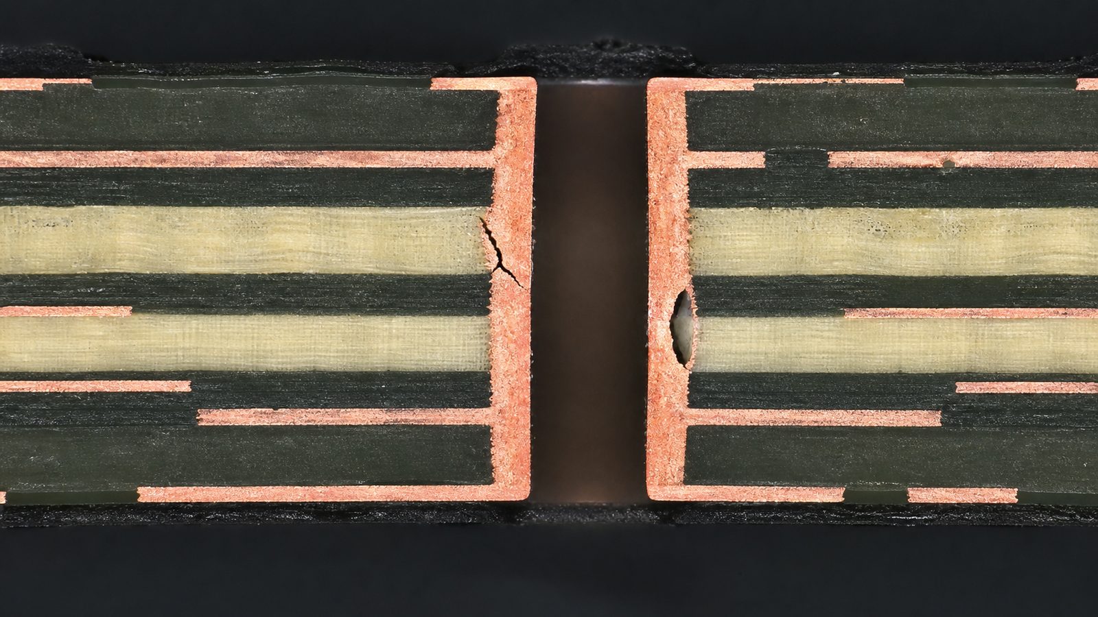
Illustrative PCB cross section showing a barrel crack and plating void for microsection defect review
Illustrative cross-section: suspicious features should be confirmed against preparation quality and the applicable acceptance criteria.

A disciplined report separates three statements: what is visibly observed, what criterion applies and what root-cause hypothesis remains to be tested. For example, “a discontinuity is visible at the knee” is an observation. “The feature does not meet drawing requirement X” is an acceptance conclusion. “Thermal stress caused the discontinuity” is a causal hypothesis that may require history, replication or additional analysis.

Microsection vs X-Ray, AOI and Electrical Test

No single inspection method covers all PCB risks; choose the method according to the physical question. Cross-sectioning gives direct material and interface evidence at one destroyed location. X-ray shows density and geometry without cutting. AOI evaluates visible surfaces. Electrical test verifies connectivity and isolation but does not explain every structural cause.

Method Best question Main limitation
Microsection What is happening inside this material interface? Destructive and highly location-dependent
X-ray Is hidden geometry, voiding or alignment suspicious? Overlapping features and material density can limit interpretation
AOI / visual inspection Are visible surfaces, patterns or components acceptable? Cannot directly see most internal interfaces
Electrical test Are intended connections present and unintended connections absent? May not reveal a structurally weak connection that still conducts
Functional test Does the assembled product perform its intended function? May locate the symptom without isolating the physical cause

A broader method-selection comparison is available in the PCB testing methods and equipment guide.

How to Read a PCB Microsection Report

A decision-ready report must connect every image and measurement to a traceable sample, target feature and acceptance requirement. Attractive microscope photographs without identification, scale or disposition are not enough for lot release or corrective action.

  • Confirm the purchase order, board number, revision, lot and sample identity.
  • Verify whether the sample is a coupon or production board and where it came from on the panel.
  • Check preparation orientation and whether the inspected plane passes through the intended feature.
  • Require a scale bar or calibrated measurement reference on measurement images.
  • Match each reported value to a clearly marked location.
  • Separate observations from acceptance decisions and root-cause hypotheses.
  • Identify the drawing, specification revision and product class used for disposition.
  • Record whether thermal conditioning or other preconditioning occurred before sectioning.
  • Ask for a clear Pass, Fail or Engineering Review disposition with the reason.

How to Write Acceptance Criteria Into the PO and Quality Plan

Specify the governing documents, product class, coupon plan, sampling trigger, inspected features and required report content before fabrication starts. A late request for “a microsection report” can produce images that do not answer the buyer’s actual reliability concern.

Do not copy a generic numerical limit into every project. Acceptance depends on board technology, applicable IPC performance specification, customer drawing, qualification status and contract. State which document controls if requirements conflict. Also define whether a failed coupon stops the lot, triggers additional samples or requires an engineering review.

A practical PO note can request: board and lot traceability; coupon identity and panel location; specified preconditioning; defined inspection features; calibrated images; the applicable requirement beside each result; and retention of the report for an agreed period.

What to Send for a Failure-Analysis Review

Send enough evidence to preserve the failure context before anyone chooses the cut location. The most useful package includes the board revision, Gerber or ODB++ data, stackup, fabrication notes, drill information, affected net or component, symptoms, electrical measurements, thermal history, lot data and marked photographs of the suspect location.

If assembly is involved, add the BOM, CPL, assembly drawing, reflow history when available and the exact point at which the failure appeared. State whether the goal is conformance verification, root-cause investigation or process comparison; each goal may require a different sample plan.

Never cut the only failed sample before documenting it. When the defect may be intermittent, preserve electrical behavior and external condition first. The sectioning plan should be approved by the person responsible for the investigation.

How Microsection Findings Should Change Production Controls

The value of microsection analysis comes from the control change it supports, not from the microscope image itself. A confirmed issue should be traced to the relevant process window—such as drilling, desmear, plating, lamination, imaging, thermal exposure or assembly—and linked to containment, root-cause verification and corrective action.

For recurring production, compare like-for-like evidence: the same coupon design, target feature, preparation orientation, measurement definition and acceptance rule. Otherwise, apparent improvement may be caused by a changed inspection method rather than a changed process.

  1. Contain suspect lots and protect traceability.
  2. Confirm the observation with suitable repeat evidence.
  3. Identify the process variable capable of producing that structure.
  4. Change and document the control or process window.
  5. Verify effectiveness with new representative samples.
  6. Update the control plan, work instruction or supplier requirement.

FAQ About PCB Microsection Analysis

Is PCB microsection analysis destructive?

Yes. The selected coupon or board area is cut, mounted, ground and polished. Use a production coupon when possible, and document any unique failed sample before sectioning because the original condition cannot be restored.

Is microsectioning the same as cross-section analysis?

In PCB work, the terms are commonly used for the same preparation-and-inspection approach. “Microsectioning” emphasizes specimen preparation, while “cross-section analysis” emphasizes examination and measurement of the exposed plane.

Can a microsection prove that the whole PCB lot is good?

Not by itself. It directly represents the inspected sample and plane. Lot conclusions require an agreed coupon design, sampling plan, panel-location logic and acceptance rule that make the evidence representative.

Can X-ray replace PCB microsection analysis?

Not for every question. X-ray is non-destructive and useful for hidden geometry and density differences, while a microsection directly exposes material interfaces. The two methods often complement each other during failure analysis.

What standards are commonly associated with PCB microsections?

IPC-9241 addresses microsection preparation guidance, and IPC-TM-650 includes relevant preparation and dimensional inspection methods. Product acceptance normally comes from the applicable performance specification, acceptability standard, drawing and purchase requirements.

Should a coupon be thermally stressed before sectioning?

Only when the qualification or investigation plan requires it. Preconditioning can expose weaknesses that are not visible in an as-received sample, but the condition, cycle and sequence must be recorded so results remain interpretable.

What makes a microsection report traceable?

It should identify the board, revision, lot, coupon or sample, panel location when relevant, target feature, preparation orientation, image scale, measurement locations, governing requirements and final disposition.

Why can two laboratories report different measurements?

Differences may come from sample position, section plane, edge preparation, calibration, measurement definition or interpretation. A shared method, marked measurement locations and retained images make comparisons more reliable.

How do I avoid confusing an artifact with a real crack?

Check preparation quality, nearby material deformation and whether the feature persists under another viewing condition or repeat section. A real defect conclusion should not rely on one ambiguous image.

What files should accompany an RFQ that needs microsection evidence?

Send Gerber or ODB++, stackup, drill data, fabrication drawing, board class or performance requirement, coupon or sampling expectations, required preconditioning, inspection features, report format, quantity and target schedule.

Turn the Cross-Section Into a Clear Manufacturing Decision

A good microsection plan starts before cutting: define the risk, choose a representative target, control preparation and connect every observation to an agreed acceptance rule. That discipline prevents both false rejects and false confidence.

Need a PCB or PCBA quotation with defined cross-section evidence? Send EBest Circuit your Gerber or ODB++ files, stackup, drill data, quantities, product class, coupon or sampling expectation, preconditioning requirement and target delivery date. Our engineering team can review the manufacturing package and clarify which inspection evidence should be included before production. Email sales@bestpcbs.com to request a DFM and quality-plan review.

You may also like

PCB Quality Agreement Checklist for Fabrication and PCBA
Monday, August 17th, 2026
OEM and PCB supplier teams reviewing quality agreement responsibilities and board samples
A PCB quality agreement should convert expectations into named responsibilities, controlled evidence and clear release decisions before the first purchase order.

This PCB quality agreement checklist defines how a customer and PCB/PCBA supplier control specifications, acceptance, traceability, changes, nonconformance and performance. The agreement supplements the drawing, purchase order and commercial contract by assigning who must do what, which records prove it, and when customer approval is required.

This checklist is for engineering, supplier quality and purchasing teams preparing a new supplier, new product or higher-risk production program. It is not legal advice; liability, warranty, confidentiality, governing law and other legal terms should be reviewed by qualified counsel.

If a shipped board fails, can both parties point to the same approved file, acceptance rule, affected lot and corrective-action owner?

If the answer depends on assumptions scattered across quotations and emails, the quality agreement is incomplete.

EBest Circuit can review project-specific fabrication, PCBA, inspection, test and documentation requirements before quotation.

Send Gerber/ODB++, drawings, stackup, BOM/CPL when applicable, quantity, acceptance criteria, traceability depth, required records, change-control rules and target delivery. Final scope is confirmed from the released project package.

The 12 PCB Quality Agreement Clauses to Set Before a PO

Clause Required decision Observable evidence
1. Scope and roles Products, sites, processes and responsible contacts Approved responsibility matrix
2. Document authority Which file/revision governs conflicts Released package and acknowledgement
3. Engineering review DFM/EQ ownership and design authority Closed questions and approved deviations
4. Materials/sub-tier control Approved sources, substitutions and outsourced steps Source/lot/process records
5. Acceptance Inspection, test, sampling, limits and reports Job-linked results
6. Traceability/records Lot/panel/unit depth, retention and retrieval Retrievable history
7. Change notification Triggers, notice, approval and effectivity Approved PCN
8. Deviations/nonconformance Containment, authority and disposition NCR/deviation record
9. CAPA/complaints Response, root cause and effectiveness Closed corrective action
10. Audit/access Audit rights, confidentiality and record access Audit plan/findings
11. Performance Quality, delivery and escalation metrics Scorecard/review minutes
12. Continuity/exit Disaster, obsolescence, inventory and transfer Continuity/transition plan

Define Scope, Sites and Responsibility Owners

Name the legal entities, manufacturing sites, product families, bare PCB/PCBA scope, component sourcing, testing, packaging and any special process. Identify engineering, quality, purchasing and account contacts plus an escalation path. If different factories or subcontractors perform parts of the work, state who remains accountable for the finished result.

Set the Document Hierarchy and Design Authority

List the controlled inputs: purchase order, Gerber/ODB++ or IPC-2581, drill data, fabrication drawing, stackup, BOM, CPL, assembly drawing, test specification and approved engineering queries. Define which record wins when they conflict and how both parties confirm the released revision.

The supplier may propose manufacturability changes, but design authority must be explicit. Use the PCB engineering change order checklist when an approved design changes after release.

Agree on Materials, Sources and Sub-Tier Processes

Define approved laminate/material families, copper, finish, solder mask, components and any customer-controlled sources. State substitution rules, counterfeit/traceability expectations, storage/shelf-life controls and customer-supplied material responsibilities. Require control of outside finish, special processes, bare-board sources or test labs that can affect acceptance.

Write Inspection, Test and Shipment Acceptance Rules

A quality agreement should name applicable specifications, drawing requirements, sample or 100% checks, test methods, acceptance limits, required reports and shipment-release authority. Separate bare-board electrical/visual/dimensional evidence from PCBA AOI/X-ray/ICT/functional evidence. Do not use “standard inspection” when the buyer expects a specific record.

The PCB testing guide helps choose evidence matched to the build and risk.

PCB quality agreement control loop for files materials inspection testing changes records and performance
Quality responsibilities form one loop: controlled inputs, qualified materials/processes, inspection, test, change control, records, corrective action and ongoing performance.

Specify Traceability Depth, Record Retention and Retrieval

Choose shipment, lot, panel or unit traceability based on risk and customer need. Define links to material/component lots, manufacturing order, revision, process/inspection/test records, rework and shipment. State retention period, format, access, backup and expected retrieval time. Avoid promising unit-level history if the agreed process only controls lots.

Control Supplier Changes, Deviations and Nonconformance

List material, process, site, equipment, subcontractor, design/configuration and supply-status changes that require notice and approval. The PCB supplier change notification checklist provides the PCN fields and effectivity gates.

Separately define temporary deviations and nonconforming product: containment, segregation, customer notification, material-review authority, use-as-is/rework/scrap/return decisions and traceability. The supplier should never treat shipment pressure as approval.

Define Complaint, CAPA and Effectiveness Requirements

Set who acknowledges a complaint, contains affected lots, provides interim status and submits root-cause/corrective-action evidence. Do not measure closure only by report date. Require verification that the cause was removed, related products/processes were reviewed and later production confirms effectiveness. Define how repeat or major issues escalate.

Set Audit Rights, Confidentiality and Record Access

Define planned and cause-based audit rights, notice, sites/processes in scope, remote/on-site access, customer/end-customer participation, confidentiality and corrective-action follow-up. Audit access should respect sensitive supplier information while still proving control. Use the PCB supplier audit checklist to connect clauses with evidence sampling.

Measure Supplier Performance and Escalation

Agree on a small set of defined metrics: accepted/defective quantity, escapes/returns, delivery, response time, CAPA aging and repeat findings. Define data source, calculation period, review frequency and escalation thresholds. A scorecard should trigger decisions—improvement plan, controlled new business, re-audit or disqualification—not exist as decoration.

Plan Business Continuity, Obsolescence and Supplier Exit

Address disaster recovery, capacity interruption, material/component obsolescence, EOL notice, last-time buy, customer-owned inventory/tooling, unfinished WIP and controlled transfer to another site or supplier. Define what records and approved data must be returned or transferred at termination. Legal ownership and liability terms belong with qualified contract review.

What to Send EBest Circuit Before Finalizing the Quality Scope

Use this PCB quality agreement checklist when sending the PCB/PCBA part and revision, released manufacturing files, application/risk context, quantity, acceptance criteria, test/report needs, traceability depth, record requirements, change-notification rules and target delivery. For assembly, include BOM/CPL, source restrictions, programming and functional-test inputs.

EBest Circuit can review the manufacturable quality scope and quotation assumptions for the project. The final agreement should identify what is feasible, which evidence will be delivered and which customer approvals remain required.

FAQ About PCB Quality Agreements

What is a PCB quality agreement?

It is an operational agreement assigning customer and supplier responsibilities for specifications, acceptance, traceability, changes, nonconformance, records and performance.

Is a quality agreement the same as a purchase order?

No. The PO places the order; the quality agreement defines continuing quality responsibilities and evidence.

Who should approve it?

Engineering, quality and purchasing should approve their responsibilities; legal counsel should review legal/commercial terms where appropriate.

Should prototypes need the same agreement as production?

Not always. Scale controls to risk, but even prototypes need clear files, acceptance, change authority and nonconformance handling.

What traceability level should be required?

Select shipment, lot, panel or unit depth from product risk and customer/regulatory needs, then confirm the supplier can execute it.

How are supplier changes controlled?

Define PCN triggers, notice, evidence, customer approval and the first affected lot/date/PO boundary.

What happens when quality performance declines?

Use agreed metrics and escalation: containment, corrective action, improvement plan, re-audit, restricted business or disqualification.

You may also like

PCB Supplier Change Notification Checklist for Process Changes
Monday, August 17th, 2026
Supplier and customer engineers reviewing PCB process change notification samples
A useful PCB supplier change notification gives the customer enough time and evidence to assess risk before the changed product enters a shipment.

A PCB supplier change notification (PCN) is the controlled notice a PCB or PCBA supplier sends before changing an approved material, process, site, equipment route, subcontractor or product configuration. It should describe the current and proposed states, affected items, reason, risk, qualification evidence, implementation boundary and requested customer decision.

The goal is not to generate more paperwork. It is to prevent an apparently minor supplier change from altering impedance, solderability, reliability, compliance, traceability, assembly behavior or long-term availability without the customer knowing which lots are affected.

Would your team learn about a material, factory or process change before the first changed PCB lot ships—or only after a quality problem?

If the purchase order and quality agreement do not define notification triggers, timing and approval authority, both customer and supplier may assume the other party owns the decision.

EBest Circuit can review project-specific PCB/PCBA change requirements and affected manufacturing data.

Send the controlled Gerber/ODB++, drawing, stackup, BOM/CPL if applicable, approved material/process requirements, quantity, validation needs and required notice/approval rules. Final feasibility and evidence depend on the released construction and change scope.

What a PCB Supplier Must Notify Before Making a Change

A supplier should notify changes that can affect the approved definition, manufacturing route, product performance, acceptance evidence or continuity of supply. The exact trigger list belongs in the purchase agreement, drawing, specification or supplier-quality agreement; it should not depend on one salesperson deciding whether a change seems important.

Notification does not automatically mean rejection. It creates a review gate so engineering, quality and purchasing can decide whether the change is equivalent, needs evidence, requires a limited qualification build or cannot be accepted.

PCB Change Triggers That Require Customer Review

Change area PCB/PCBA examples Customer question
Material Laminate, prepreg, copper foil, solder mask, surface finish chemistry, adhesive or approved component source Does form, fit, function, reliability or compliance change?
Process or equipment Lamination route, drilling/plating method, imaging, cleaning, soldering, rework, test or inspection method Is the output still controlled to the approved requirement?
Site or ownership Factory move, new line, merger, tooling transfer or different manufacturing entity Does qualification and traceability remain valid?
Subcontractor New outside finish, special process, bare-board source or assembly partner Who controls the external process and its records?
Design/configuration Stackup, panel, marking, BOM alternate, firmware or test limit proposed by the supplier Who has design authority to approve it?
Supply status Discontinuance, allocation, EOL material or emergency substitution What inventory and transition plan protects continuity?

PCN, ECO, Deviation and SCAR: Do Not Mix the Records

A PCN starts with the supplier and asks the customer to review a proposed product or process change. An engineering change order usually authorizes a customer-controlled design change. A deviation requests temporary permission to depart from an approved requirement. A supplier corrective action request (SCAR) addresses a failure and asks for root cause and corrective action.

One issue may require several linked records, but each has a different decision. The PCB engineering change order checklist covers customer-originated design release; this page controls supplier-originated change notice and approval.

Set Notice Timing by Contract and Risk, Not One Universal Number

There is no single notice period that fits every PCB program. Define the required advance notice in the contract or quality agreement and align it with qualification time, inventory exposure, regulatory/customer approval and supply continuity. A high-reliability material or site change may need more review than a documentation correction.

Emergency changes caused by obsolescence, disaster or sudden material unavailability still require prompt disclosure, containment and an agreed interim plan. “Emergency” should not silently turn a proposed substitution into an approved change.

Required Fields in a PCB Supplier PCN Template

PCN field Minimum useful content Approval value
Identity PCN number, supplier site, customer, affected part numbers/revisions and contacts Creates traceability
Current vs proposed state Specific before/after material, process, site, source or configuration Shows the real difference
Reason and risk Driver, urgency, known effects and potential failure modes Supports priority and depth
Affected scope Orders, inventory, WIP, finished lots and related products Defines containment
Qualification Test plan, comparison data, samples and acceptance criteria Makes equivalence observable
Effectivity Proposed date, PO, lot, date code or serial boundary Prevents mixed shipments
Decision Approve, reject, request evidence, limited approval or deviation Records authority and conditions

Assess Form, Fit, Function, Reliability and Supply Impact

Review the change against the released requirement, not only the supplier’s statement that it is “equivalent.” Check physical dimensions and interfaces, electrical behavior, thermal/mechanical performance, process compatibility, solderability, impedance, environmental/compliance documentation, inspection/test coverage, marking, traceability and service interchangeability.

Also review business impact: new tooling, MOQ, price, lead time, lifecycle, remaining old stock and the risk of splitting production between old and new states. A technically acceptable change can still create an uncontrolled supply transition.

PCB supplier material process site and component changes routed through approval and validation
Material, process, site, subcontractor and component changes should converge at one controlled impact review before qualification and the first changed lot.

Route the PCN Through Engineering, Quality and Purchasing Approval

Engineering assesses design and performance impact. Quality defines qualification, traceability and acceptance evidence. Purchasing assesses price, inventory, continuity and contract terms. Regulatory or customer-program owners join when their requirements are affected. Assign one coordinator and one final authority rather than collecting disconnected email opinions.

Record open questions, owner, due date and disposition. The supplier should not implement the changed state until the required decision is issued, unless a documented emergency/deviation path explicitly authorizes it.

Define Qualification Evidence Before Approving the Change

Evidence should target the changed risk. A material/stackup change may require updated construction, impedance or reliability review. A finish or soldering-process change may require solderability, microsection, profile or assembly evidence. A site/equipment transfer may require first-article comparison and process capability evidence. A component-source change may need authenticity, package, electrical, lifecycle and functional review.

Define sample size, method, limits and records before testing. Use the PCB testing guide to distinguish bare-board from assembly evidence, and use the PCB supplier audit checklist when the change also affects site or process qualification.

Control Effectivity, Existing Inventory and the First Changed Lot

Approval should state which lot, date code, PO or serial number first uses the change. Identify old material, WIP and finished inventory, then decide whether it may be used, segregated, returned, reworked or exhausted under a controlled boundary. Require the first changed lot to carry the agreed identification and evidence package.

After approval, update drawings, specifications, approved-source records, incoming inspection and supplier records. Monitor early lots for the failure modes considered in the impact assessment.

Put Change-Notification Rules Into the PCB Quality Agreement

  • define product/material/process/site/subsupplier and supply-status triggers;
  • state the required advance notice or emergency escalation path;
  • name customer and supplier contacts plus approval authority;
  • prohibit implementation before required approval;
  • define PCN fields, evidence, sample and document format;
  • set effectivity, inventory, traceability and first-lot rules;
  • define what happens when a change is implemented without notice;
  • require flow-down to relevant sub-tier suppliers.

The custom PCB supplier guide helps connect these controls to RFQ and supplier selection.

What to Send EBest Circuit for a Controlled PCB Change Review

Send the affected PCB/PCBA part and revision, current and proposed state, reason, target timing, open orders, inventory/WIP status and required approval process. Include Gerber/ODB++, fabrication drawing, stackup and material/finish requirements; add BOM, CPL, assembly drawing, test and programming data for PCBA.

State the validation evidence you require and whether any customer, regulatory or service approval is involved. EBest Circuit can review project-specific feasibility, manufacturing impact and quotation, but the released files and agreed acceptance plan remain the basis of approval.

FAQ About PCB Supplier Change Notifications

What does PCN mean in PCB manufacturing?

PCN commonly means product or process change notification: a supplier’s controlled notice of a proposed change affecting an approved PCB or PCBA.

Which PCB changes require a PCN?

Define triggers contractually; typical areas include material, process, site, equipment route, subcontractor, source, product configuration, test and supply status.

Is a PCN the same as an ECO?

No. A PCN usually originates with a supplier; an ECO authorizes a controlled engineering design change.

How much advance notice is required?

Use the purchase/quality agreement and applicable customer or regulatory requirement. Do not assume one universal period.

Can a supplier implement a change before approval?

Only if the governing agreement allows it or a documented emergency/deviation approval authorizes it.

What should be checked in the first changed lot?

Confirm identification, approved effectivity, targeted qualification evidence, traceability and any enhanced inspection or test.

What if a supplier changed a process without notice?

Contain affected lots, identify the implementation boundary, assess risk, request records and decide disposition plus corrective action.

You may also like

PCB Supplier Audit Checklist for Fabrication and PCBA
Monday, August 17th, 2026
Quality engineers auditing PCB factory process evidence and board quality
A supplier audit should connect claimed capability to controlled processes, sampled records and closed corrective actions.

A PCB supplier audit checklist helps buyers verify whether a fabrication or PCBA supplier can repeatedly build the actual product—not whether its presentation looks impressive. The audit should test factory ownership, process control, traceability, inspection, change management, subcontracting and corrective action with current evidence.

Use it before awarding a high-risk program, after a major process/site change, when performance deteriorates, or when the product moves from prototype to production. Scale depth to board and application risk.

Can the supplier trace one shipped lot backward from test result to materials, process records, approved data and operators?

If not, certificates and equipment lists cannot prove control of your order.

EBest Circuit can support project-specific manufacturing review and evidence requests.

Send Gerber/ODB++, drawing, stackup, quantity, test/document needs and supplier-audit questions. Add BOM, CPL and acceptance criteria for PCBA. Exact capability remains subject to the released construction.

Decide Audit Scope From Product Risk

Define site, product family, processes and evidence period before scheduling. Consider technology complexity, safety/reliability consequence, volume, prior escapes, new equipment, special processes and subcontractors. A remote document audit may screen a supplier; critical work may require process observation and record sampling.

Request Evidence Before the Audit

  • legal entity, site address, organization and manufacturing/subcontracting map;
  • quality certificates with site, scope, issuer and validity;
  • process flow, control plan, inspection/test plan and sample traveler;
  • equipment, calibration, maintenance and capability evidence relevant to the proposed build;
  • material approval, storage, shelf-life and lot-trace procedures;
  • document/change control, nonconformance, CAPA and complaint procedures;
  • recent delivery, quality and corrective-action performance;
  • data security, business continuity and disaster-recovery controls.

Verify Factory Ownership and Subcontractors

Match the quotation to the physical site that performs each step. Identify who controls CAM, imaging, lamination, drilling, plating, solder mask, finish, routing, electrical test, SMT/THT, cleaning, programming and functional test. For every outsourced special process, verify approval criteria, incoming acceptance, traceability and change notification.

A trading office can provide useful service, but the buyer must know who owns product quality and who can retrieve original process evidence.

Audit QMS, Document Control and Change Authority

Sample one current job. Confirm the operator used the approved revision, traveler, stackup, work instructions and inspection limits. Check obsolete-file removal, access control, backup, retention and customer approval for material, stackup, process, site or subcontractor changes. The PCB CAM guide explains why front-end edits need visible authority.

Trace Materials From Receiving to Shipment

Select a finished lot and walk backward. Verify laminate/copper or component identity, supplier, receipt, inspection, lot/date code, storage condition, shelf-life controls, issue-to-job record and remaining inventory. Check how substitutions and customer-supplied material are segregated and approved. Do not accept a generic certificate that cannot be tied to the audited lot.

Review PCB Fabrication Process Controls

Process Audit evidence Failure to challenge
Imaging/etching Artwork revision, setup, inspection and trend records Width/spacing or registration drift
Drilling/plating Tool life, bath control, coupon/microsection and acceptance Hole quality and interconnect risk
Lamination Approved stackup, material lot, press cycle and verification Thickness, registration or reliability variation
Finish/profile/test Process control, dimensions, electrical test and final records Solderability, fit or escaped opens/shorts

Audit only the processes relevant to the proposed construction; confirm capability from evidence, not a universal marketing maximum. Use the DFM checklist to connect design risks to factory controls.

PCB supplier audit control loop covering factory materials process inspection and performance
Qualification is a loop: verify site, material, process and inspection, then monitor performance and corrective action.

Review PCBA Controls When Assembly Is Included

Check BOM/CPL/program revision control, approved component sources, moisture sensitivity, ESD, solder paste and stencil control, feeder setup, first-article approval, reflow profile, selective/manual soldering, AOI/X-ray rules, rework authorization, cleaning, programming and functional test. Confirm defect data can be traced to line, lot, machine/program and disposition.

Sample Inspection, Test and Calibration Records

Choose records yourself rather than accepting a prepared example. Confirm equipment ID, calibration status, method, limits, result, sample size, failure handling and job/lot link. Review the PCB testing guide when deciding which evidence fits bare boards versus assemblies.

Test Nonconformance and CAPA With a Real Example

Follow one defect from detection through segregation, material review, customer notification, root cause, containment, corrective action, effectiveness check and recurrence prevention. Weak systems close actions when a report is issued; strong systems prove the cause was removed and related products/processes were reviewed.

Turn Findings Into Approval, Conditions or Rejection

Classify findings by product risk and systemic weakness. Record requirement, objective evidence, affected process, owner and due date. Approval options should be explicit: approved; conditionally approved with limited scope/quantity and CAPA; development supplier requiring verification; or rejected. Do not average a critical traceability failure away with high scores for housekeeping.

Monitor the Supplier After Approval

An audit is a baseline, not permanent approval. Review incoming defects, escapes, returns, delivery, responsiveness, deviations, change notifications, CAPA aging and repeat findings. Define re-audit triggers and require renewed evidence after site/process/ownership changes. The custom PCB supplier guide helps connect qualification to project RFQs.

FAQ About PCB Supplier Audits

What should a PCB supplier audit cover?

Factory identity, QMS, documents, materials, fabrication/assembly controls, inspection/test, calibration, traceability, subcontractors, changes, CAPA and performance.

Can a remote audit replace an onsite audit?

It can screen documents and records, but observation and independent sampling may be needed for high-risk processes.

How often should a PCB supplier be audited?

Set frequency from risk and performance; re-audit after major changes, repeated defects or serious escapes.

Are certificates enough?

No. Verify site/scope/validity, then sample how the system controls real jobs.

How do I verify traceability?

Select a finished lot and trace it backward to data revision, materials, operations, inspections and dispositions.

What is a critical audit finding?

A failure that threatens product safety, legality, identity, traceability, design authority or reliable process control.

What should I send EBest for qualification?

Send Gerber/ODB++, drawing, stackup, quantity, test/report needs and your supplier-quality questions; add BOM/CPL for PCBA.

You may also like

PCB Assembly First Article Inspection: Prove the Build Before Production
Saturday, August 15th, 2026
Engineer performing first article inspection on a newly assembled PCB
A first article is valuable only when it is built to the released baseline, inspected against defined characteristics, and held for a documented decision.

PCB assembly first article inspection is a documented production gate that checks whether the first build represents the released design and manufacturing package before more units are allowed to proceed. It is not a ceremonial photograph of one completed board and it is not a substitute for process control or product validation.

The inspection should connect the revision, parts, placement, solder, mechanics, programming, test, deviations, and approval state. Its exact scope depends on product risk, customer requirements, volume, novelty, and the evidence already created during design and prototype validation.

Will the first article report let an engineer decide “build, correct, or stop” without guessing which revision, part lot, measurement, test program, or deviation produced the unit?

If not, the report is an inspection scrapbook rather than a production-release record.

EBest Circuit can review Gerber or ODB++, BOM, AVL, CPL/centroid, drawings, approved deviations, inspection characteristics, programming and test requirements, quantity, traceability, and approval workflow before confirming a project-specific first article plan.

No universal EBest FAI form, sampling level, measurement system, report standard, or approval scope should be assumed without that review.

Use First Article Inspection as a Production Gate

Define the hold point, responsible reviewer, required evidence, response time, and permitted work while approval is pending. The gate should stop the defect multiplier: a wrong revision, rotated part, unapproved substitute, incorrect program, or mechanical mismatch should be found before the same error reaches the full lot.

State whether only the first unit is held, whether a small setup quantity may be built, and which operations must wait. Production urgency does not remove the need for a clear release authority.

Separate FAI From Prototype Testing and Routine Inspection

A prototype proves design questions, routine inspection monitors production, and FAI verifies that a defined manufacturing baseline produced an acceptable representative unit. These activities can share evidence but they do not have identical purposes.

A prototype hand-built with temporary parts may not represent the production route. The prototype-to-production assembly page explains why the manufacturing handoff needs its own controls.

Freeze the Revision and Acceptance Baseline

List every controlled input used for the first article. Include PCB fabrication data, assembly drawing, schematic reference, BOM/AVL, CPL or centroid, polarity data, mechanical model, work instructions, programs, test specifications, approved deviations, and customer notes.

Record revision identifiers and release dates. A report cannot prove conformance when it references “latest files” or combines documents from different releases.

Verify the Bare PCB and Fabrication Inputs

Confirm the board identity and the fabrication characteristics that can affect assembly or fit. Review part number and revision, outline, thickness where required, holes and slots, finish, markings, panel or breakaway condition, damage, cleanliness, and any controlled dimensional or electrical records.

The FAI need not repeat every supplier inspection, but it must identify the evidence relied upon and verify characteristics critical to the assembled product.

First article inspection gate from inputs and build through inspection test and approval
Inputs, build, inspection, test, and approval form a gate; skipping the baseline makes later evidence ambiguous.

Reconcile BOM, AVL, Lot, and Substitution Status

Compare every fitted and intentionally unpopulated reference against the released BOM and approved source list. Verify manufacturer part, value, package, quantity, lot/date code restrictions, customer-supplied material, substitutions, and deviation authorization.

A correct-looking package can still be the wrong electrical grade or source. Link component evidence to the first unit and preserve the comparison method.

Inspect Placement, Polarity, Orientation, and Hardware

Check reference designators, presence, absence, polarity, pin-one, orientation, offsets, seating, connector alignment, fasteners, spacers, heat sinks, labels, and other mechanical items against released data. Include manual and secondary operations, not only SMT placement.

The AOI quality guide helps separate automatable visible checks from characteristics that require another method or human judgment.

Evaluate Solder Joints and Hidden Connections

Use inspection methods matched to joint visibility and product risk. Visible solder can be assessed for wetting, bridging, opens, excess, insufficiency, disturbance, and damage; hidden BGA, QFN, bottom-terminated, or shielded joints may need suitable indirect or X-ray evidence.

Do not claim that a top-side photograph proves a hidden interface. The automated X-ray inspection guide explains what buyers should specify and what X-ray cannot prove alone.

Measure Mechanical, Fit, and Interface Requirements

Identify dimensions and interfaces that can stop enclosure fit, mating, cooling, fastening, optical alignment, cable routing, or service access. Define datum, tool, method, tolerance, unit, sample, and record for each required characteristic.

Use the actual assembly state required by the drawing. A measurement taken before hardware installation may not predict the completed product.

Verify Programming, Electrical Test, and Product Function

Record firmware or configuration identity, programming result, fixture and program revision, limits, measured data where required, and first-pass/final outcome. Include continuity, power, interface, calibration, or functional checks appropriate to the product.

The PCB assembly testing services guide helps define fixtures, limits, logs, retest, and failure disposition.

Build a First Article Report That Supports a Decision

For each controlled characteristic, show the requirement, source, method, result, status, evidence reference, reviewer, and disposition. Add unit identity, build date, PCB lot, component lots as required, document revisions, equipment identification where applicable, photographs, test files, deviations, and signatures or electronic approvals.

Structure the report so a reviewer can distinguish “not required,” “not inspected,” “not measurable,” “failed,” and “passed.” Blank cells are not evidence.

First article inspection evidence covering BOM placement solder test and deviations
BOM, placement, solder, test, and deviation evidence must point to the same unit and released baseline.

Contain Deviations Before More Units Are Built

When the first unit does not conform, stop affected work, identify scope, preserve evidence, and route the issue to the authorized owner. Record the requirement, actual result, affected unit, suspected cause, correction, reinspection, test, and decision.

Do not quietly edit the report, replace a part, or rerun a test until it passes. First-pass evidence helps distinguish setup errors, design ambiguity, component issues, and unstable process conditions.

Define Approval, Conditional Approval, and Rejection

Use explicit states with explicit permissions. Approval may release the defined production scope; conditional approval should list open items, quantity/time limits, containment, owner, and due date; rejection should identify the hold and required corrective evidence.

Link approval to the exact unit and baseline. An email saying “looks good” is risky when it cannot be connected to the report revision and unresolved deviations.

Trigger Re-FAI When a Change Can Alter the Result

Define which changes require full or partial first article repetition. Examples may include PCB revision, component substitution, footprint or program change, new fixture, process route change, new manufacturing location, long production gap, corrective action, or customer-directed review.

Use risk and affected characteristics to set the scope. Preserve the relationship between original approval, change record, new evidence, and release.

Compare FAI Quotes by Evidence and Hold Time

Normalize planning, setup quantity, inspection characteristics, measurement programming, AOI/X-ray or other evidence, electrical/functional test, report format, engineering review, customer hold time, corrections, reinspection, and exclusions. First article inspection cost depends on evidence scope, not just one board.

Ask what happens while approval is pending and how schedule changes if the first unit fails. A low FAI price may exclude the measurements or report the customer actually expects.

Send an RFQ Package That Defines First Article Release

Provide one controlled package. Include PCB and assembly data, BOM/AVL, CPL, drawings, schematic reference, mechanical model, workmanship and dimensional requirements, approved substitutions, critical characteristics, programming, test, traceability, report format, approver, response time, production hold, quantity, forecast, and delivery date.

Use the traceability requirements guide to define how the first unit, files, material, process, inspection, test, deviation, and approval remain linked.

PCB Assembly First Article Inspection FAQ

What is the purpose of first article inspection?
It verifies that the released design and manufacturing package produced an acceptable representative unit before broader production is released.

Is FAI the same as prototype testing?
No. Prototype work answers design questions; FAI verifies a defined production baseline and route, although some evidence may be reused.

Does FAI mean inspecting every feature?
The required characteristics come from product risk, drawings, specifications, customer requirements, and the agreed plan; do not assume a universal scope.

What documents should be frozen?
Freeze PCB data, BOM/AVL, CPL, drawings, programs, test requirements, deviations, and any acceptance sources used by the build.

Should hidden solder joints be inspected?
Use a method appropriate to visibility and risk; a top-side image alone cannot prove a hidden interface.

What should an FAI report contain?
Include unit identity, baseline revisions, requirements, methods, results, evidence, status, deviations, reviewers, and approval.

Can production continue while FAI is pending?
Only within the explicitly agreed hold and risk rule. Define what may proceed, quantity limits, and who accepts that risk.

When is re-FAI required?
Repeat the affected scope when a design, material, program, fixture, route, location, corrective action, or other change can alter the approved result.

Does EBest use one universal FAI standard and report?
No default should be assumed. Submit the customer and product requirements so scope, evidence, report, and approval can be confirmed.

What files are needed for an FAI quote?
Send PCB and assembly files, BOM/AVL, CPL, drawings, deviations, critical characteristics, programming, test, traceability, quantity, and schedule.

You may also like

Moisture-Sensitive Device Handling in PCB Assembly: From Receipt to Reflow
Saturday, August 15th, 2026
Moisture-sensitive electronic components in dry packaging beside a controlled PCB assembly line
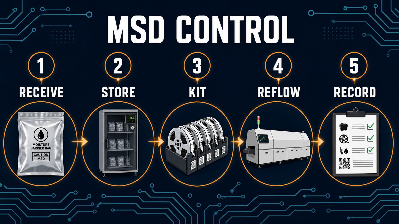
Moisture control is a chain of custody: label, dry pack, exposure clock, storage, kitting, reflow, and record must agree.

Moisture sensitive device handling PCB assembly controls protect plastic-packaged components from absorbed moisture that can expand during soldering and damage internal interfaces. The risk is difficult to manage after the fact because an affected package may show no obvious external warning before reflow.

A practical plan identifies sensitive parts, verifies packaging, starts exposure at a defined event, controls storage and kitting, handles uncertain material, and carries the history through reflow, rework, and shipment. Exact limits come from the current component label, manufacturer instructions, customer requirements, and approved handling standard.

Can your assembler show the remaining exposure allowance for each opened reel at the moment it reaches reflow?

If the answer depends on memory, a handwritten date without a time, or a shared estimate for several split reels, the process cannot reliably distinguish usable material from uncertain material.

EBest Circuit can review BOM, AVL, manufacturer part numbers, supplier labels, packaging condition, assembly route, reflow exposure, lot-traceability requirement, quantity, and schedule before confirming a project-specific moisture-control plan.

No dry-cabinet condition, bake profile, floor-life limit, resealing method, or equipment capability should be assumed without that review.

Identify Moisture-Sensitive Parts Before They Reach the Line

Map each manufacturer part number to the current moisture classification and handling instruction supplied for that exact package. Record the approved source, package type, lot, date code, label data, dry-pack status, and any customer-specific controls.

Do not infer one requirement from a similar component family or distributor description. A package change, alternate source, or revised manufacturer notice can change the applicable handling route. The component sourcing service page explains why source and part identity must remain connected to assembly planning.

Inspect Dry Packs, Labels, Desiccant, and Indicators at Receipt

Receiving should verify that the part, lot, quantity, label, sealed bag, desiccant, humidity indicator where required, and accompanying instructions are consistent. Check for tears, punctures, weak seals, missing fields, water damage, or evidence that the package has already been opened.

Capture the condition before warehouse relabeling. If a supplier label is covered or discarded, the assembly team may lose the only direct link to the original moisture status.

Quarantine Missing or Contradictory Moisture Data

Uncertain material is a disposition problem, not a production scheduling problem. Hold parts when the label, indicator, bag condition, exposure history, part number, or lot record is missing or contradictory. Engineering, quality, sourcing, and the customer can then choose an approved route.

Do not reset a clock by creating a new internal label. A new label can improve traceability only when it preserves the verified prior history.

Start the Exposure Clock at a Defined Event

Define exactly when controlled dry storage ends and exposure begins. The trigger may be bag opening or another event specified by the approved method; record date, time, operator, material identity, location, and applicable allowance.

The same rule must cover bags opened for inspection, sampling, relabeling, programming, or partial kitting. A reel should not receive a fresh allowance simply because it moves to another department.

Moisture-sensitive device control flow from receipt and storage through kitting reflow and recording
Receipt, storage, kitting, reflow, and recording must preserve one component identity and one exposure history.

Store Sealed and Opened Material Under Separate Rules

A sealed verified dry pack and an opened reel are different inventory states. Define locations, environmental controls, identification, access, monitoring, alarm response, and record requirements for each state. Prevent ordinary warehouse stock from being mistaken for controlled open material.

Storage equipment does not repair an unknown history. Its conditions and recovery assumptions must come from an approved procedure, not a generic rule copied from another product.

Build Kitting Around Remaining Floor Life

Kit only the quantity and timing that the line can consume within the approved remaining allowance. Coordinate setup, feeder loading, line stops, changeovers, inspection holds, maintenance, and expected reflow time rather than treating placement as the finish point.

Use first-expiring material deliberately and keep the reel identity visible at the feeder. A complete kit is not production-ready if its most constrained component will expire before soldering.

Link Reel Splits and Partial Lots to One Exposure History

When a reel, tray, or tube is divided, each child container must retain the parent part, manufacturer, lot, date code, quantity, moisture data, opening time, prior exposure, and remaining status. Barcodes or system records are useful only when the join is reliable.

Do not let a partial reel return to stock with a new local identifier that hides its earlier exposure. The PCB assembly traceability guide shows how component, process, and test records should connect.

Coordinate Staging, Placement, and Reflow Windows

Plan to the point of thermal exposure, not merely feeder load. Queue time, line balance, inspection, double-sided assembly, selective operations, interruptions, and weekend holds can consume the allowed window.

Record the actual route and define what happens when a board or component waits longer than planned. The lead-free PCB assembly guide explains why material handling and thermal planning must be coordinated rather than optimized separately.

Bake Only Under an Approved Component-Specific Route

Baking is not a universal reset button. Confirm that the exact component, carrier, packaging, terminals, labels, trays, tapes, and reels can tolerate the selected route, and follow the current manufacturer or customer-approved instruction.

Define authorization, equipment, loading, time, temperature, maximum repetitions when applicable, cooling, handling after bake, new status, and records. Excessive or inappropriate baking can create other material or solderability risks.

Reseal Returned Material With Its Remaining-Life Record

Line return should preserve, not restart, the history. Record removal time, consumed quantity, remaining exposure, condition, desiccant and indicator requirements, reseal event, operator, and new controlled-storage location.

Use packaging appropriate to the approved method and protect labels from being separated from the reel. Recounting inventory does not replace exposure reconciliation.

Moisture-sensitive device handling risks including open bag humidity mixed lots over-bake and missing records
Open bags, uncontrolled humidity, mixed lots, unsuitable baking, and missing logs turn moisture status into an assumption.

Contain Expired, Damaged, or Uncertain Material

Stop and identify all affected containers and assemblies when the allowed exposure is exceeded or the history cannot be proven. Preserve labels, times, environmental records, line location, affected board serials or lots, and any completed reflow.

Disposition may include approved recovery, inspection, test, customer review, scrap, or another documented action. Do not blend uncertain parts with verified stock or process them simply to avoid a line stop.

Keep Moisture History Through Rework and Second-Side Reflow

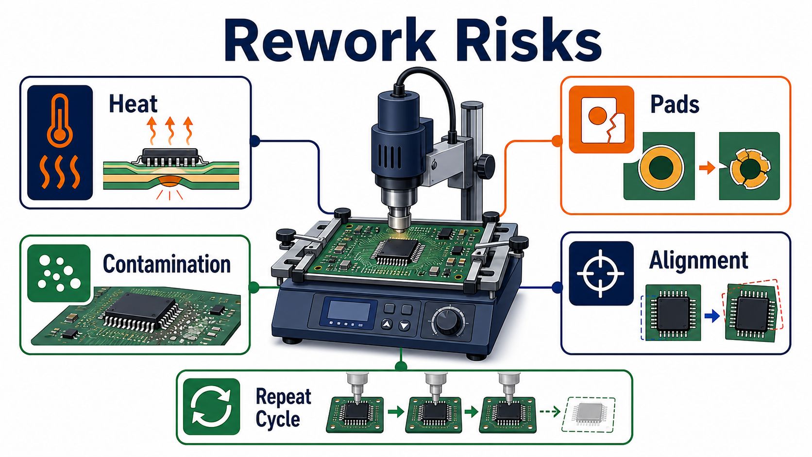
Additional thermal cycles and repair handling require their own review. Account for assemblies waiting between sides, packages exposed during troubleshooting, replacement components opened for rework, and any component-specific restrictions.

The BGA soldering guide provides useful context for moisture-sensitive packages and reflow evidence. Link rework material and results back to the affected assembly.

Compare Assembly Quotes by Included MSD Controls

Normalize receiving inspection, controlled storage, exposure tracking, partial-reel handling, line staging, approved recovery, resealing, traceability, reporting, and exclusions. One quote may include ordinary warehouse handling while another includes a project-specific control plan.

Ask who supplies dry packaging, how opening and return events are recorded, what creates a production hold, who approves baking, and which records ship with the product.

Send an RFQ Package That Defines Moisture Handling

Provide one revision-controlled package. Include PCB and assembly files, BOM and AVL, manufacturer part numbers, approved alternates, lot/date-code restrictions, supplier packaging and label requirements, classification data, customer standard, assembly sides, reflow route, line timing, recovery approval, traceability, test, quantity, forecast, and delivery target.

State whether the customer expects per-reel, per-lot, or per-serial evidence. The PCBA manufacturing guide helps align these component controls with the full build route.

Moisture-Sensitive Device Handling FAQ

What makes an electronic component moisture sensitive?
Its package can absorb moisture that may expand during soldering and stress internal package interfaces; use the exact manufacturer classification and handling data.

When does floor-life exposure begin?
Use the event defined by the approved handling method and record it consistently, including bags opened for inspection or partial kitting.

Can a new label restart the exposure clock?
No. Relabeling must preserve verified prior history; it cannot create new remaining life.

Should every opened reel be baked?
No. Bake only when the exact part and packaging have an approved route and the material status requires it.

What happens when a reel is split?
Each child container needs the parent identity, lot, moisture data, opening time, prior exposure, quantity, and remaining status.

Does dry storage erase earlier exposure?
Do not assume so. Apply the approved rule for the exact component and preserve the full history.

Why track reflow time instead of placement time?
The critical plan must include staging, line stops, inspection holds, and the actual path to the relevant thermal cycle.

How should uncertain material be handled?
Quarantine it, preserve evidence, identify affected assemblies, and obtain documented engineering or quality disposition.

Does EBest publish universal dry-cabinet or bake settings?
No. The capability source does not confirm those settings; the project must be reviewed against component and customer requirements.

What should be sent for an MSD-controlled quote?
Send PCB data, BOM/AVL, manufacturer parts, moisture labels or requirements, assembly/reflow route, quantity, traceability, test, and schedule.

You may also like

Conformal Coating Inspection for PCB Assembly: Coverage, Defects, and Release
Saturday, August 15th, 2026
Conformal coating inspection of a PCB assembly under controlled lighting
A useful coating inspection proves the specified areas are protected while connectors, contacts, test points, and other keep-outs remain usable.

Conformal coating inspection PCB assembly planning must begin before material is applied. A glossy board is not automatically a protected board: the coating can miss a critical edge, bridge into a connector, trap contamination, remain uncured, or hide damage that existed before coating.

This guide gives buyers and engineers a release path from incoming assembly condition through masking, application, cure, inspection, test, repair, and traceable acceptance. Exact material, method, thickness, cure, and equipment must be confirmed for the project rather than assumed from a general quote.

Can your supplier show where coating is required, where it is forbidden, and what evidence releases each assembly?

If the answer is only “visual inspection,” the RFQ is missing the drawing boundaries, defect criteria, cure evidence, test plan, and repair rules needed to compare suppliers.

EBest Circuit can review Gerber or ODB++, BOM, assembly drawings, coating and masking requirements, component constraints, quantity, inspection evidence, test requirements, and delivery target before confirming project-specific support.

The coating material, thickness, application method, cure process, inspection equipment, and acceptance standard are not universal capabilities and must be agreed for the actual build.

Define the Coating and Inspection Requirement Before Production

Release a controlled requirement that identifies the coating material or approved family, coverage zones, keep-outs, thickness basis when applicable, cure condition, appearance limits, inspection method, and acceptance authority. Link it to the correct assembly revision and product environment.

A purchase order line that says “apply conformal coating” leaves the supplier to guess which surfaces, components, edges, vias, connectors, test points, and hardware need protection or exclusion. That uncertainty becomes a quote gap and a production dispute.

Inspect PCB Assemblies Before Coating Starts

Coating should not become a cover for existing defects or contamination. Verify assembly revision, cleanliness requirement, component presence and orientation, solder condition, damage, markings, connectors, test status, and any customer hold points before masking or coating.

Record pre-coat acceptance when later investigation would be difficult. The broader PCBA manufacturing guide shows why inspection and test gates must be planned as one route rather than added at shipment.

Turn the Masking Drawing Into an Inspectable Boundary

Mark every keep-out with a clear datum, dimension, component reference, or controlled image. Common exclusions may include connector contacts, mating surfaces, switches, sockets, grounding points, test pads, programming contacts, heat-transfer interfaces, optical windows, labels, or adjustment features.

Define allowable edge variation and what counts as coating intrusion. A vague red cloud on a screenshot is hard to measure and harder to reproduce after a revision change.

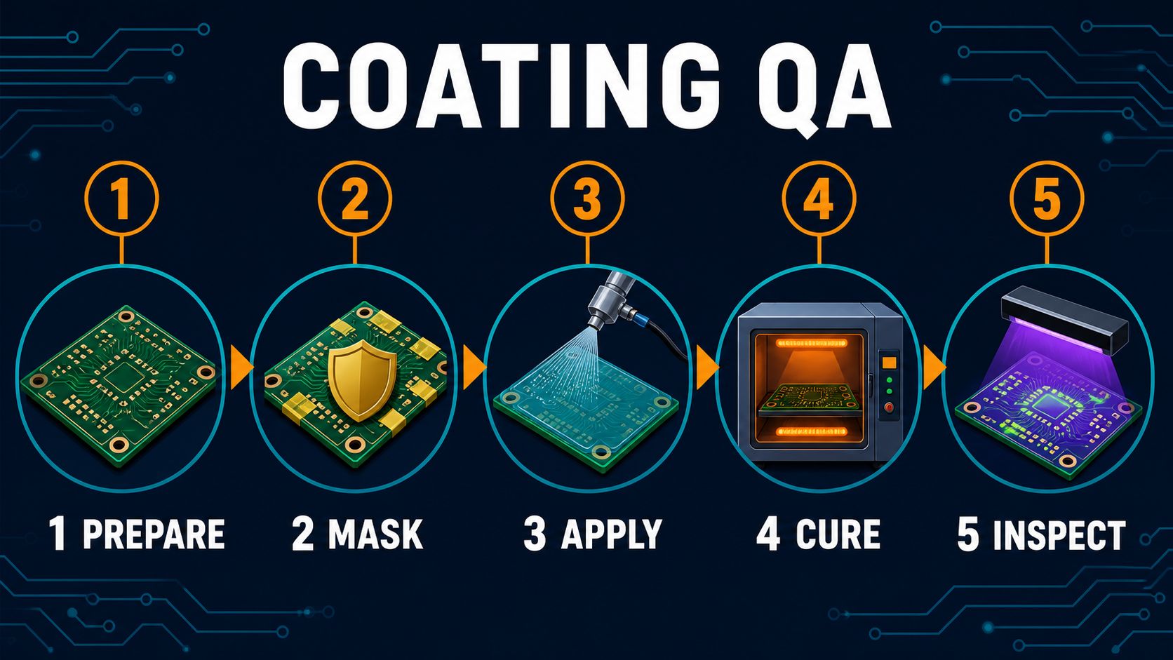
Control Coating Preparation, Application, and Cure Records

Inspection begins with process identity. Record the material lot and expiry where required, mix or preparation status, viscosity or environmental checks when specified, application method, program or operator, time, cure route, and any hold between steps.

Do not copy generic temperature, time, or humidity values into the RFQ. Use the selected material data, product limitations, customer requirements, and an approved work instruction.

Conformal coating quality flow from preparation and masking to application cure and inspection
Preparation, masking, application, cure, and inspection create one evidence chain; a missed upstream control cannot be repaired by a final glance.

Check Coverage Without Hiding Keep-Out Violations

Inspect both required coverage and forbidden coverage. Confirm the board side, component bodies, leads, solder joints, edges, corners, and local zones named by the drawing, while checking that coating has not entered contacts, test points, fastener surfaces, or other keep-outs.

Use a route that prevents inspectors from focusing only on bright, easy-to-see surfaces. Coverage must be evaluated against the released map, not against the appearance of a nearby “good” board.

Separate Cosmetic Variation From Functional Defects

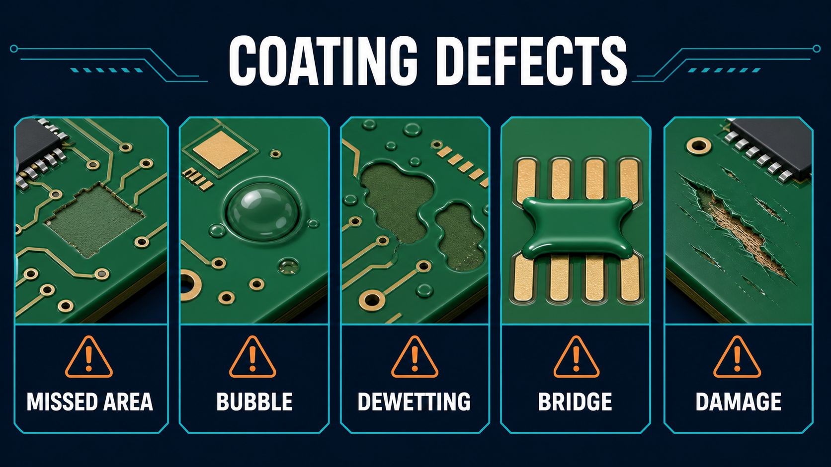
Define which conditions affect protection, electrical behavior, mechanical fit, cure, adhesion, or future service. Typical review categories include missed areas, thin or heavy zones, bubbles, voids, dewetting, fisheyes, runs, pooling, cracks, contamination, fibers, bridging, overspray, lifting, discoloration, and damage.

Names alone are insufficient. Specify location, size or extent where needed, risk, disposition, and whether the condition can be repaired. Do not reject harmless variation or accept a functional keep-out violation because both are called “appearance.”

Use UV, White Light, and Magnification for Different Questions

No single viewing condition answers every inspection question. UV response can help reveal coverage for compatible materials; white light shows color, contamination, pooling, masking residue, and physical damage; magnification helps evaluate edges, leads, bubbles, cracks, and small intrusions.

Inspection performance depends on the selected coating and board. Define lighting, viewing access, magnification, reference samples, and evidence capture where the product risk requires them. The AOI quality guide explains why automated optical results also depend on detectable features and programmed criteria.

Treat Thickness and Cure as Specification-Driven Evidence

Measure thickness only with a method, location, timing, and acceptance range suitable for the selected coating and assembly. A wet-film reading, dry-film result, coupon, witness panel, or other method answers a different question; the RFQ must state which evidence is required.

Cure verification may rely on approved time and environment records plus inspection or test defined by the material and customer. “Dry to the touch” is not a universal release criterion.

Inspect Under Components, Leads, Edges, and Shadowed Areas

Plan access for areas that are difficult to see after application. Tall components, close stand-offs, lead rows, connectors, board edges, heat sinks, mechanical hardware, and dense local geometry can create shadows, capillary flow, pooling, or incomplete penetration.

Decide whether these areas require direct viewing, angled optics, a witness feature, a process validation, or a documented exception. Do not promise complete under-component coverage unless the design, material, method, and acceptance approach support it.

Conformal coating defect map showing missed area bubble dewetting bridge and handling damage
Useful defect categories connect a visible condition to location, product risk, disposition, repair, and reinspection.

Test the Assembly After Coating Without Damaging the Evidence

Repeat the electrical or functional checks needed to show that coating, masking removal, cure, and handling did not change performance. Define accessible test interfaces before coating and protect them according to the masking plan.

State limits, fixture, program, data retention, retest, and failure disposition. The PCB assembly testing services guide helps buyers distinguish structural inspection from electrical proof.

Control Repair, Touch-Up, and Reinspection

A coating repair is a controlled process, not an invisible cosmetic edit. Authorize the defect, protect the assembly, remove or prepare material as approved, correct the cause, reapply the selected coating, cure it, reinspect the full affected zone, and repeat required testing.

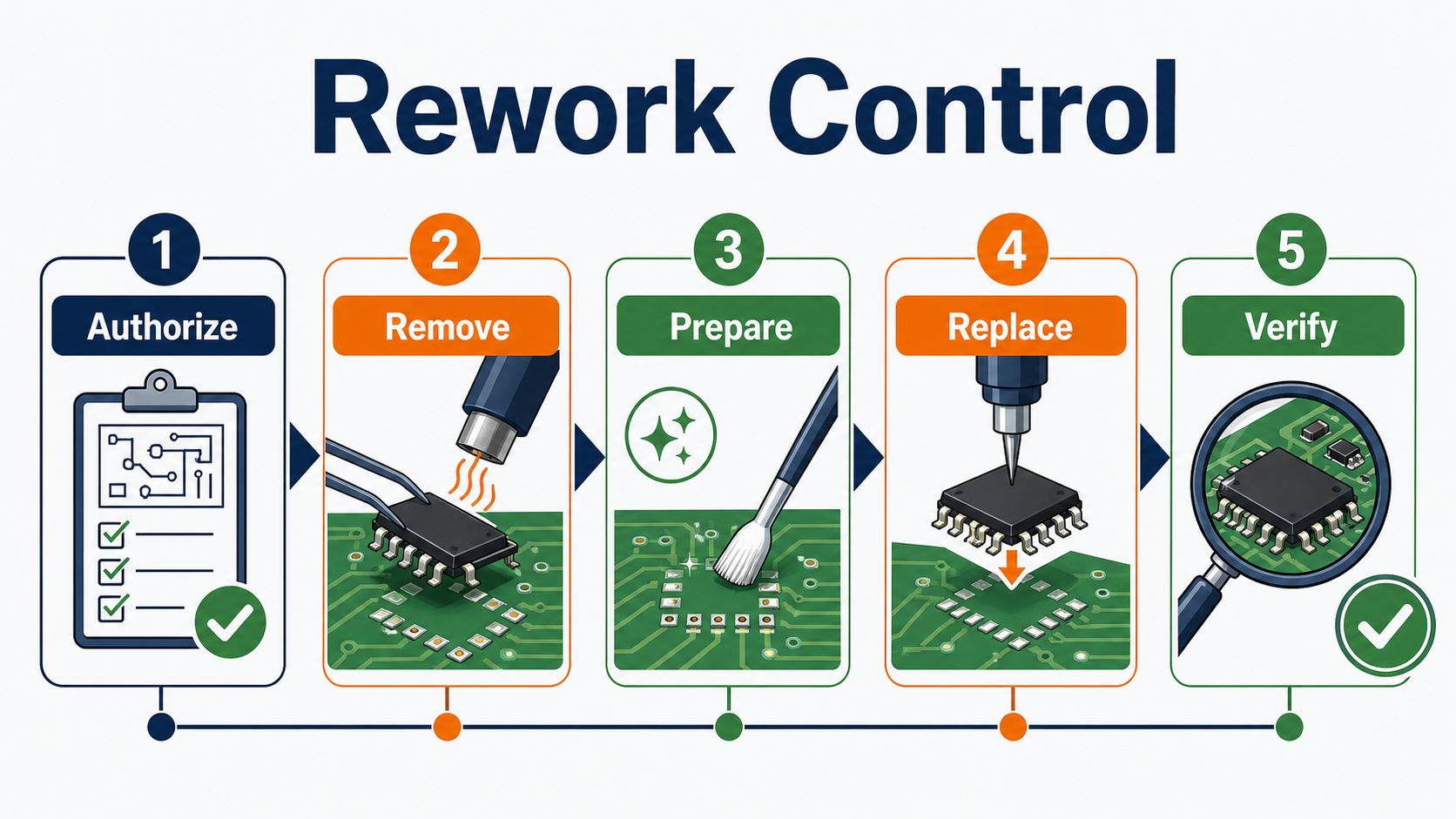
Record repair count, location, material, operator, date, inspection, and disposition when traceability is required. Use the PCB assembly rework process to structure authorization and release evidence.

Link Coating Evidence to the Correct Lot or Serial Number

Traceability should connect the assembly revision, coating material lot, work instruction, process date, inspection result, repair, test, and shipment identity at the level the customer requires. Preserve both first-pass and final acceptance when failures or repairs matter.

The PCB assembly traceability requirements guide helps define the join keys and retention scope before quoting.

Compare Conformal Coating Quotes by Included Evidence

Normalize material sourcing, cleaning or preparation, masking labor and tooling, application method, cure, inspection, thickness evidence if specified, test, traceability, samples, repair, packaging, NRE, and exclusions. A low unit price may omit masking complexity or post-coat test.

Ask whether the quote assumes customer-supplied material, validated drawings, reusable masks, witness coupons, special handling, or a fixed batch size. Compare the deliverable evidence, not only the coating name.

Send an RFQ Package That Defines Coating Release

Provide one revision-controlled package. Include PCB and assembly data, BOM and AVL, drawings, selected coating or approval route, environmental objective, keep-out map, component restrictions, cleaning requirement, application and cure constraints, coverage and defect criteria, thickness evidence if required, inspection method, test, traceability, quantity, packaging, and schedule.

Ask the supplier to mark every assumption and exclusion. EBest Circuit will review the submitted package and confirm what can be supported for the specific project.

Conformal Coating Inspection FAQ

What should be inspected before conformal coating?
Verify revision, cleanliness requirement, assembly defects, component condition, markings, connectors, test status, and any customer hold point before masking.

Does UV light prove coating thickness?
No. UV response can help reveal coverage for compatible materials, but thickness needs a specified measurement method and location.

Which areas are usually masked?
The drawing may exclude contacts, connectors, switches, sockets, test points, grounding or heat-transfer surfaces, labels, optics, and adjustment features.

Are bubbles always rejectable?
Not by name alone. Acceptance depends on size, location, extent, coating specification, product risk, and the released defect criteria.

How do inspectors find missed coating?
They use the approved coverage map with suitable white light, UV when compatible, magnification, viewing angles, and evidence capture.

Should assemblies be tested after coating?
Use the product-specific electrical or functional checks needed to prove that coating, cure, masking removal, and handling did not change performance.

Can coating be repaired?
Yes when an approved repair route defines preparation, material, cure, reinspection, test, and traceability; do not treat touch-up as an undocumented cosmetic action.

How is conformal coating thickness specified?
Define the selected material, required range, measurement method, location, timing, coupon or witness approach, and disposition rules.

Does EBest use a default coating material and inspection machine?
No default should be assumed. Submit the project requirements so material, application, cure, inspection, and test scope can be reviewed and confirmed.

What files are needed for a conformal coating quote?
Send PCB and assembly data, BOM, drawings, coating and masking requirements, component constraints, quantity, inspection evidence, test, traceability, packaging, and delivery target.

You may also like

Press-Fit PCB Assembly Process: Hole Control, Insertion, and QA
Saturday, August 15th, 2026
Press-fit PCB assembly with a supported board connector and controlled insertion press
Press-fit assembly depends on the complete system: compliant pin, finished plated hole, board support, alignment, insertion cycle, and verification.

A press fit PCB assembly process creates an electrical and mechanical connection by inserting compliant pins into controlled plated through holes without soldering the joint. Success depends on matching the connector specification to the finished-hole geometry, supporting the board, aligning every pin, monitoring insertion, and verifying the finished assembly.

This guide helps engineers and buyers prepare a press-fit RFQ without assuming that a generic drill size, connector name, or press setting will work for every board.

Can the supplier prove that the pin, finished hole, board support, and insertion cycle form one controlled process?

A connector may look seated while one pin is folded, one hole is damaged, or the board has flexed. Define input specifications and release evidence before production.

EBest Circuit can review the customer’s connector data, PCB files, hole requirements, mechanical model, insertion specification, quantity, and acceptance plan before confirming project-specific support.

No EBest finished-hole tolerance, pin compatibility, force limit, press equipment, or yield should be assumed without that review.

What the Press-Fit PCB Assembly Process Must Control

The process must protect hole integrity, pin geometry, board structure, seating, and electrical performance. Control the released connector, plated-hole requirement, PCB revision, fixture, orientation, insertion sequence, force or displacement evidence where required, inspection, test, and traceability.

Press-fit is not simply “push until seated.” The connection relies on elastic interaction between the compliant section and the plated hole, so both component and PCB data are manufacturing inputs.

Confirm the Connector and Compliant-Pin Specification First

Use the exact manufacturer part number and current application specification. Record pin style, approved hole range, board thickness or engagement constraints, insertion tool, seating reference, force guidance, repair rules, and any keep-out or support requirements.

Do not substitute a visually similar connector or infer compatibility from nominal pitch. Approved alternates need engineering review and revision control.

Translate Pin Data Into Finished-Hole Requirements

The connector specification usually applies to the finished plated hole, not only the mechanical drill. The fabrication drawing must communicate the finished-hole requirement, plating context, tolerance, and inspection method agreed for the selected part.

Drill size, plating, material behavior, and process variation interact. The verified EBest capability source contains no press-fit-specific entry, so this article does not publish a universal EBest value. The design should be reviewed against the connector data and actual PCB construction.

Design the PCB Layout for Access and Mechanical Support

Provide space for the connector, insertion tool, fixture, board support, and inspection. Keep nearby components, tall hardware, connectors, and underside features clear of the press path and support points.

Review copper, planes, hole-to-feature spacing, board edges, cutouts, stackup, and mechanical loads. The PCB design constraints guide explains why fabrication and assembly limits must be coordinated before release.

Inspect Boards and Connectors Before Insertion

Screen inputs before a press cycle converts an input defect into board damage. Verify part number, orientation, pin condition, hole pattern, board revision, cleanliness, damage, warpage, and required measurements or records.

Protect pins during handling. Bent, contaminated, missing, or previously inserted connectors need disposition before loading.

Build a Fixture That Supports the Board Near the Connector

The fixture should react insertion load without excessive board bending. Support close to the hole field while clearing underside pins, components, solder joints, and tooling features. Use stable datums and prevent reversed loading.

A fixture that supports only the panel edges can allow local flex, laminate stress, or damage to neighboring assemblies. Validate support on the actual board, not a simplified outline.

Press-fit PCB process from hole specification and support through alignment insertion and verification
Hole requirements, local support, pin alignment, controlled insertion, and verification are one linked process.

Align Every Pin Before Force Is Applied

All pins must enter the intended holes without side load or tilt. Use connector and board datums, guiding features, visual checks, or tooling appropriate to the design. Begin with controlled engagement and stop if resistance appears abnormal.

Do not use increasing force to overcome misalignment. A single bent pin can damage plating, enlarge a hole, tilt the connector, or create a latent intermittent connection.

Insert the Connector With a Controlled Press Cycle

Apply load through the approved connector surface and insertion tooling. Control speed, travel, seating reference, parallelism, and stop condition as required by the connector and assembly plan.

Prevent contact with housings or features not designed to carry insertion load. Monitor the board and connector throughout the cycle; unusual sound, tilt, force, or travel requires containment.

Use Force-Displacement Data as Process Evidence

When required, force-displacement monitoring can show whether the cycle followed the approved signature. Define which values or curve features are recorded, how limits are established, how connector pin count affects interpretation, and what happens after an out-of-limit result.

A curve is evidence only when linked to the correct unit, connector, fixture, program, and acceptance rule. Do not publish or apply generic force limits across different connectors.

Inspect Seating, Pins, Holes, and Board Condition

Post-insertion inspection should confirm seating and check for damage introduced by the operation. Inspect connector height or seating feature, tilt, exposed compliant sections where applicable, bent or missing pins, board cracks, mask damage, laminate stress, and nearby components.

Access to both sides and the exact criteria depend on the assembly. Record the result against the lot or serial identity.

Test Electrical Continuity and Product Function

Mechanical seating does not prove electrical performance. Define continuity, isolation, signal, power, programming, or functional checks appropriate to the connector’s role. Preserve first-pass and final results.

The PCB assembly testing services guide helps define limits, logs, retest, and failure disposition. Broader assembly handoff is covered in the PCBA manufacturing guide.

Press-fit PCB risks including hole size board flex pin damage tilt and repair
The process must contain hole, board, pin, alignment, and repair risks rather than relying on final appearance.

Control Removal, Repair, and Repeat Insertion Risk

Removal is a separate engineered process. Define extraction tooling, board support, connector disposition, hole inspection, allowable replacement, electrical verification, and repeat-cycle rule. Do not assume a hole or pin remains acceptable after extraction.

The PCB assembly rework process guide explains authorization, evidence preservation, site inspection, test, and release.

Compare Press-Fit Assembly Quotes and Exclusions

Normalize connector sourcing, PCB review, hole inspection, fixture NRE, tooling, press programming, cycle evidence, per-unit insertion, inspection, test, traceability, removal, repair, and exclusions. Two prices are not comparable if one assumes customer-supplied validated tooling while the other includes development.

Ask who owns and maintains the fixture, how connector changes are handled, and how out-of-limit cycles are dispositioned.

Send a Press-Fit RFQ Package Suppliers Can Review

Provide one revision-controlled package. Include PCB fabrication and assembly data, stackup, finished-hole callout, connector data, mechanical model, insertion tool and seating requirements, fixture concept, quantity, forecast, press evidence, inspection, electrical/functional test, traceability, repair rule, packaging, and target date.

Use the traceability guide to define how connector lot, PCB lot, program, curve, inspection, and test are linked.

Press-Fit PCB Assembly Process FAQ

What is a press-fit PCB connection?
It is a solderless connection made when a compliant pin is inserted into a controlled plated through hole.

Is press-fit the same as through-hole soldering?
No. The electrical/mechanical interface comes from the compliant pin and plated hole rather than a solder joint.

Should the drawing specify drill size or finished hole?
The connector requirement normally relates to the finished plated hole; fabrication data must also define the process inputs needed to achieve it.

Why is local board support important?
It reacts insertion load near the connector and reduces flex and stress on the board and neighboring components.

What causes bent press-fit pins?
Misalignment, damaged input parts, hole mismatch, tilted tooling, inadequate guidance, or forcing an abnormal cycle can bend pins.

Is force monitoring always required?
Not universally. Use it when the connector, product risk, customer, or process plan requires it and define the acceptance logic.

How is seating verified?
Use approved mechanical/visual criteria, pin inspection, board condition checks, and electrical or functional test.

Can a press-fit connector be removed and reused?
Do not assume so. Follow connector guidance and engineering disposition for the pin, hole, board, and replacement process.

Can EBest publish a universal press-fit hole tolerance?
No. The original capability source has no press-fit entry; the exact connector, hole, plating, stackup, and process require project review.

What files are needed for a quote?
Send PCB data, stackup, connector specification, hole requirements, mechanical model, fixture/insertion criteria, quantity, test, traceability, and schedule.

You may also like

PCB Assembly Rework Process: Control Heat, Evidence, and Release
Saturday, August 15th, 2026
Controlled PCB assembly rework process under microscope with localized heating
Controlled rework starts with authorization and ends with documented inspection, testing, and disposition.

A PCB assembly rework process should correct one authorized condition without creating hidden damage elsewhere. The work must control sample identity, component removal, localized heat, pad condition, replacement alignment, cleaning, inspection, electrical or functional verification, and the release record.

Rework is not the same as diagnosis or unrestricted repair. This guide shows buyers and engineers how to define the work, acceptance checks, repeat-cycle limits, and RFQ evidence before a supplier touches the assembly.

Will the board be more reliable after rework—or merely appear to pass?

Ask which defect is authorized, how existing evidence is preserved, what thermal and mechanical risks apply, which acceptance criteria release the unit, and how prior heat cycles remain traceable.

EBest Circuit can review a customer’s affected units, assembly data, defect description, approved instruction, component information, acceptance criteria, and required test before confirming project-specific support.

Do not assume package, coating, hidden-joint, heat-cycle, equipment, certification, or yield capability before the actual board and scope are reviewed.

What a Controlled PCB Assembly Rework Process Must Achieve

Successful rework restores the authorized requirement while protecting the surrounding assembly. It should leave traceable evidence of the original defect, work performed, replacement material, inspections, test result, and final disposition.

A visual improvement alone is not enough. The board must meet the same functional and quality intent used to release acceptable production, plus any rework-specific checks for pads, adjacent parts, contamination, coating, and prior heat exposure.

Decide Whether to Rework, Repair, Use As Is, or Scrap

Disposition comes before tooling. Rework returns an assembly to the drawing or specification; repair may use an authorized method that differs from the original design; use-as-is accepts a documented deviation; scrap removes the unit from use.

Review product risk, defect mechanism, accessibility, replacement availability, board value, prior cycles, hidden damage, acceptance authority, and verification cost. A technically possible action may still be a poor lifecycle decision.

Authorize the Exact Unit, Defect, and Work Instruction

The instruction must identify the board, revision, location, defect, permitted action, materials, tools, settings or process window, acceptance checks, and approval authority. Prevent operators from extending one authorization to neighboring defects or additional units without review.

Record serial or lot identity and link the instruction to the controlled revision. The traceability requirements guide explains how this supports containment and later retrieval.

Preserve Original Evidence Before Touching the Board

Photograph and document the as-received condition before cleaning, heating, or removing parts. Preserve first-failure logs, inspection images, firmware, component lot, reflow history, and earlier interventions.

If the cause is not confirmed, complete or coordinate the investigation first. The failure-analysis service guide shows why premature rework can destroy the evidence needed to prevent recurrence.

Remove Coating, Adhesive, or Hardware Without Creating Damage

Access preparation is part of the rework risk. Identify coating, underfill, staking, adhesive, shields, heat sinks, connectors, and mechanical supports around the target. Define compatible removal and restoration methods.

Inspect after access is created. Scratches, lifted mask, damaged traces, displaced neighbors, residue, or mechanical stress must be contained before heat is applied.

Choose Tools and a Thermal Strategy for the Actual Assembly

Tooling should fit package geometry, board construction, copper mass, nearby components, and heat sensitivity. Consider board support, preheat, localized heat, nozzle, airflow, contact method, extraction, shielding, temperature monitoring, and cooling.

A generic setpoint is not a thermal profile. The relevant result is controlled heating that achieves removal or soldering without exceeding agreed limits or adding unnecessary cycles. Lead-free assemblies may need specific process review; see the lead-free PCB assembly guide.

PCB rework control sequence from authorization through removal preparation replacement and verification
Every stage needs a defined input, authorized action, and release check.

Remove the Component Without Lifting Pads or Disturbing Neighbors

Removal begins only after solder is adequately released. Excess force can lift pads, tear barrels, distort the board, or transfer heat to adjacent components. Use controlled extraction and stable support rather than prying.

After removal, preserve the component when analysis or lot traceability requires it. Document visible damage and inspect adjacent parts that were exposed to heat, airflow, tools, or mechanical load.

Clean and Inspect the Site Before Replacement

The landing site must be suitable for another soldering cycle. Remove residual solder and approved flux or contamination without thinning pads, damaging mask, or leaving debris. Inspect pads, traces, vias, mask, laminate, and planarity.

Stop if copper is lifted, pads are missing, laminate is discolored or delaminated, barrels are damaged, or the site no longer matches the approved instruction. Do not hide site damage under a new component.

Place and Solder the Replacement Component

Verify the replacement part, lot, orientation, moisture or handling status, and approved source before placement. Apply the authorized solder or flux method, align to the land pattern, support the board, and execute the controlled thermal sequence.

Inspect surrounding components after cooling. Clean only as required by the approved process and restore removed coating, staking, shielding, or hardware when the work instruction calls for it.

Control BGA, QFN, and Other Hidden-Joint Rework

Hidden-joint packages require controls beyond surface appearance. Define removal, site preparation, component preparation, paste or flux method, alignment, thermal process, cooling, inspection, and acceptance.

Imaging may support verification, but its scope and criteria must be agreed. The X-ray inspection guide explains how to frame hidden-joint evidence. Do not assume every anomaly or void automatically rejects the unit.

PCB assembly rework risks including heat pad damage contamination alignment and repeat cycles
Localized rework can introduce thermal, pad, cleanliness, alignment, and cumulative-cycle risks that must be controlled.

Inspect and Test the Reworked Assembly

Release checks should address both the original defect and new risks introduced by rework. Use the applicable visual, dimensional, optical, imaging, continuity, electrical, programming, or functional checks defined in the instruction.

Preserve first-pass and post-rework results. The PCB assembly testing services guide helps define limits, logs, retest, and failure disposition.

Record Parts, Heat Cycles, Results, and Disposition

The record should identify who changed what, why, how, and with what result. Capture board identity, defect code, instruction revision, removed and replacement part, lot where required, date, operator or authorization, thermal cycle, inspection, test, and disposition.

Define a repeat-rework limit or escalation rule. Repeatedly heating the same location without an engineering review can accumulate damage while erasing the original failure history.

Compare Rework Scope, NRE, Risk, and Exclusions

Normalize quotations by the work and evidence included. Compare intake engineering, setup or fixture NRE, coating or hardware removal, component sourcing, programming, per-unit work, inspection, hidden-joint verification, testing, reporting, scrap handling, shipping, and exclusions.

Ask how non-reworkable units are handled and who authorizes expanded scope. Low unit price is not comparable if it excludes site damage, replacement material, verification, or documentation.

Send a Rework Package Suppliers Can Execute

A quote-ready package should remove ambiguity before the boards move. Include affected quantity and identities, failure description, root-cause status, photos, design and assembly data, replacement components, approved instruction, coating and mechanical details, test procedure, acceptance criteria, prior heat/rework history, report needs, and target schedule.

For a new design or first build, use NPI manufacturing to validate the baseline and prevent the same rework from becoming a recurring production step.

PCB Assembly Rework Process FAQ

What is PCB assembly rework?
It is an authorized process that returns an assembly to the released drawing or specification by correcting a defined nonconformance.

What is the difference between rework and repair?
Rework restores the original requirement; repair may use an approved method that differs from the original design.

Should root cause be known before rework?
When prevention matters or evidence may be lost, investigate first. Emergency containment still needs documented authorization and preserved evidence.

Can every component be reworked?
No. Feasibility depends on package, board, damage, access, coating, prior cycles, product risk, replacement availability, and acceptance criteria.

Why is preheat used?
When appropriate, it can reduce thermal gradients and localized demand. The actual strategy must match the assembly.

How are lifted pads handled?
Stop and obtain an engineering disposition. Do not conceal pad or trace damage under the replacement component.

How is BGA rework verified?
Use the agreed combination of process records, optical checks, suitable imaging, electrical test, and functional test.

How many times can a board be reworked?
There is no universal count. Define an engineering review or limit from board construction, component, location, history, and risk.

What records should be retained?
Keep identity, reason, instruction, removed/replacement material, work date, authorization, thermal cycle, inspection, test, and disposition as required.

What files are needed for a rework quote?
Provide photos, identities, design/assembly data, defect and cause status, replacement parts, instruction, coating/mechanics, acceptance tests, quantity, and deadline.

You may also like

PCB Assembly Failure Analysis Service: From Symptom to Corrective Action
Saturday, August 15th, 2026
PCB assembly failure analysis using microscopy electrical probing and X-ray evidence
Failure analysis should preserve the unit, reproduce the symptom, eliminate competing explanations, prove root cause, and connect the finding to corrective action.

A PCB assembly failure analysis service should deliver more than a list of possible defects. It should protect the evidence, reproduce the reported symptom, select the least destructive checks first, distinguish design, process, component, firmware, and fixture causes, and show why the final root-cause conclusion fits the evidence.

The investigation scope depends on the symptom, sample quantity, product history, available records, acceptable destructive work, and decision the customer must make. This guide explains how to prepare a failure-analysis RFQ and how to judge whether the resulting report can support containment and corrective action.

Can the investigation prove why the PCBA failed without destroying the only useful evidence too early?

Before cleaning, reworking, powering, updating firmware, or removing parts, record the as-received state and agree on the test sequence. An uncontrolled first action can erase residue, thermal evidence, intermittent behavior, solder condition, or software state.

EBest Circuit can review the build files, manufacturing records, symptom description, failed samples, and requested deliverables before confirming project-specific support.

Send Gerber or ODB++, BOM, CPL, schematic where permitted, firmware and checksum, test logs, serial/lot history, photos, environmental history, known-good samples, failure rate, allowed destructive methods, and required report. Specialized laboratory methods must be confirmed for the actual case rather than assumed.

What a PCB Assembly Failure Analysis Service Must Deliver

The service should connect symptom, evidence, mechanism, root cause, affected population, and corrective action. A useful report states what was received, how samples were identified, which checks were performed, what each result means, which hypotheses were eliminated, and what additional uncertainty remains.

The final conclusion should be proportional to the evidence. “Possible solder issue” may be a screening observation; it is not a root cause. Root cause explains the condition and the process, design, material, software, or handling path that created it.

Preserve the Failed Unit Before Evidence Is Lost

Treat every returned board as evidence. Photograph packaging and the as-received unit, record serial number and revision, protect electrostatic-sensitive parts, preserve contamination, and document any mechanical damage or signs of prior repair.

Do not automatically clean, bake, power, reflash, reseat connectors, or touch suspect joints. Define who may operate the sample and under what safe conditions. If the unit is hazardous, burned, swollen, wet, or mechanically compromised, isolate it and apply an appropriate safety plan before analysis.

Define the Symptom and Reproduce It Safely

A precise symptom is the investigation’s first measurement. Record operating state, input voltage, load, temperature, communication, timing, firmware, peripherals, mechanical position, and failure signature. “Board dead” is insufficient if the actual observation is an overcurrent trip after a specific command.

Reproduction should use current limits, monitored rails, controlled fixtures, and an approved sequence. Compare the failed unit with a known-good unit under the same conditions. If the fault is intermittent, record frequency and triggers rather than repeatedly stressing the board until a new failure is created.

Build a Timeline From Manufacturing and Field Records

The failure timeline can reveal what the physical sample cannot. Connect component lots, PCB lot, assembly revision, process history, inspection, programming, test, rework, shipment, installation, usage, and field event.

The PCB assembly traceability requirements guide explains how unit identity supports this lookup. Compare failures by lot, date, line, program, supplier, component, location, operating hours, and symptom. A cluster can identify a population at risk before the laboratory work is complete.

Start With Visual, Electrical, and Non-Destructive Checks

Begin with methods that preserve the sample for later tests. Useful early work may include external visual inspection, microscopy, resistance and diode-mode comparisons, controlled power observation, thermal imaging, current signature, connector checks, optical inspection, and suitable imaging.

Review the existing production evidence before generating new data. The AOI guide shows what visible assembly information may already exist. Note that a passed production test only proves the conditions and limits executed at that time.

Separate Design, Process, Component, Firmware, and Fixture Causes

Organize hypotheses by cause family to avoid blaming the first visible anomaly. A burned component may be the result of an upstream short, incorrect power sequence, firmware command, fixture connection, contamination, or inadequate thermal margin.

PCBA failure cause map covering design process component firmware and fixture causes
The investigation should test competing cause families instead of treating the most visible damage as the original cause.
Cause Family Evidence to Compare Typical Control Question
Design Margins, startup, loads, protection, layout, thermal path Can the same symptom be produced on known-good hardware?
Process Inspection, profiles, recipes, handling, contamination, repair Does the finding cluster by lot, station, or operation?
Component Lot, source, value, damage, electrical behavior Is the part cause, contributor, or casualty?
Firmware File, checksum, configuration, logs, sequence Does a controlled software state change the symptom?
Fixture/system Cables, contacts, loads, instruments, peripherals Does the failure follow the board or the setup?

Use X-Ray and Imaging for Hidden Assembly Evidence

Imaging can examine joints or structures that are not visible from the surface. The question should identify the package, interface, defect mechanism, view, comparison sample, and acceptance basis. Imaging alone may show an anomaly without proving electrical consequence.

The automated X-ray inspection guide explains hidden-joint planning. For failure analysis, correlate images with electrical location, symptom, design geometry, known-good boards, and later physical evidence when authorized.

Authorize Cross-Section or Other Destructive Work Carefully

Destructive analysis should answer a specific question that non-destructive work cannot resolve. Mark the target, record the pre-cut condition, define orientation and depth, preserve reference samples, and agree on custody of the remaining material.

Do not section the only failed joint simply because a laboratory method is available. First confirm that location correlates with the symptom and that the customer accepts losing the original structure. Record preparation artifacts separately from true failure features.

Correlate Findings Across Failed and Known-Good Units

A comparison set prevents normal variation from being labeled a defect. Include failed units with the same symptom, failed units with different symptoms, known-good units from the affected lot, and known-good units from a stable baseline when available.

Keep identities and histories separate. If all samples are pooled or unlabeled, the investigation cannot connect a physical finding to production condition or field behavior. Sample selection should support the decision, not merely increase count.

Prove Root Cause Instead of Listing Possibilities

Root cause requires converging evidence. The proposed mechanism should explain the symptom, location, timing, affected population, physical evidence, and comparison results. A confirmation test, controlled recreation, design calculation, process correlation, or targeted experiment may strengthen the conclusion.

Separate confirmed root cause from contributing factor and unverified hypothesis. Also state limitations: unavailable records, altered samples, insufficient quantity, intermittent behavior, or methods outside scope.

PCBA failure analysis flow from symptom through root cause to corrective action
A defensible analysis moves from the observed symptom to a proven mechanism and then to an action that prevents recurrence.

Contain the Affected Lot While Analysis Continues

Do not wait for a final report before controlling a credible risk. Identify potentially affected lots or serial ranges, hold unshipped material, preserve samples and records, define temporary screening, and communicate the containment boundary.

Temporary screening is not permanent corrective action. It should have a documented detection limit, false-pass risk, ownership, release authority, and exit condition. The PCBA test-plan guide helps define executable screens and evidence.

Turn Root Cause Into Corrective and Preventive Action

Corrective action must change the condition that created the failure. Actions may affect design, material, supplier control, work instruction, process recipe, handling, fixture, firmware, inspection, test, or change management.

Define owner, implementation date, affected revisions, verification method, sample size, acceptance criteria, and effectiveness review. The action is incomplete if the team cannot show that the failure mechanism was removed or reduced and that no new risk was introduced.

Define the Failure Analysis Report and Evidence Package

Specify the report before the investigation begins. Request sample inventory, as-received photographs, procedure, equipment or method identification as applicable, raw observations, annotated images, electrical data, comparisons, hypothesis table, conclusion strength, limitations, and corrective-action recommendations.

Decide whether physical samples, sections, removed parts, images, and electronic data must be returned. Link every result to the correct sample identity and record revision.

Compare Scope, Sample Needs, Lead Time, and Exclusions

Quotations are comparable only when they investigate the same question. Normalize intake review, reproduction work, included non-destructive methods, destructive authorization, sample quantity, known-good comparisons, engineering hours, external laboratory work, report level, meetings, shipping, and exclusions.

Ask how additional work is approved if the initial evidence is inconclusive. A low entry price may cover inspection only, while a higher quote may include controlled reproduction, hypothesis testing, and an actionable report.

Send a Failure Analysis RFQ That Can Be Executed

Package the investigation like a controlled engineering job. Include unit and lot identities, revisions, symptom, operating conditions, failure frequency, safety concerns, manufacturing/test records, design files, firmware, field history, prior interventions, sample list, known-good baseline, allowed destructive methods, required conclusion, report format, and deadline.

If lead-free soldering or thermal history is relevant, include solder alloy, paste, profiles, repair history, and handling conditions; the lead-free PCB assembly guide provides useful process context.

PCB Assembly Failure Analysis Service FAQ

What is PCBA failure analysis?
It is a controlled investigation that links a board-level symptom to evidence, failure mechanism, root cause, affected population, and corrective action.

Should a failed board be reworked before analysis?
Usually not until the as-received state is documented and the plan is approved. Rework can remove the evidence needed to explain the failure.

Why start with non-destructive methods?
They preserve the unit for later comparisons and targeted destructive work. The sequence should move from broad, evidence-preserving checks to focused confirmation.
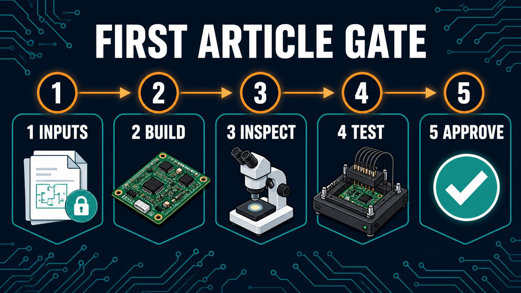
Does an X-ray anomaly prove root cause?
No. It must correlate with the electrical symptom, location, comparison units, and an accepted failure mechanism.

How many samples are needed?
It depends on failure variation, rate, available evidence, and decision. Provide multiple failed and known-good units when possible.

What is the difference between failure mode and root cause?
Failure mode describes how the unit failed; root cause explains the condition and path that created that failure.

Can firmware cause an apparent assembly failure?
Yes. Firmware, configuration, programming, and fixture behavior can produce symptoms that resemble hardware defects, so they must be controlled.

What records help the investigation?
Unit genealogy, component lots, revisions, process records, inspection, programming, test logs, rework, shipment, and field history can narrow the affected population.

What should a failure-analysis report include?
It should include sample identity, methods, observations, comparisons, eliminated hypotheses, conclusion, evidence strength, limitations, and corrective recommendations.
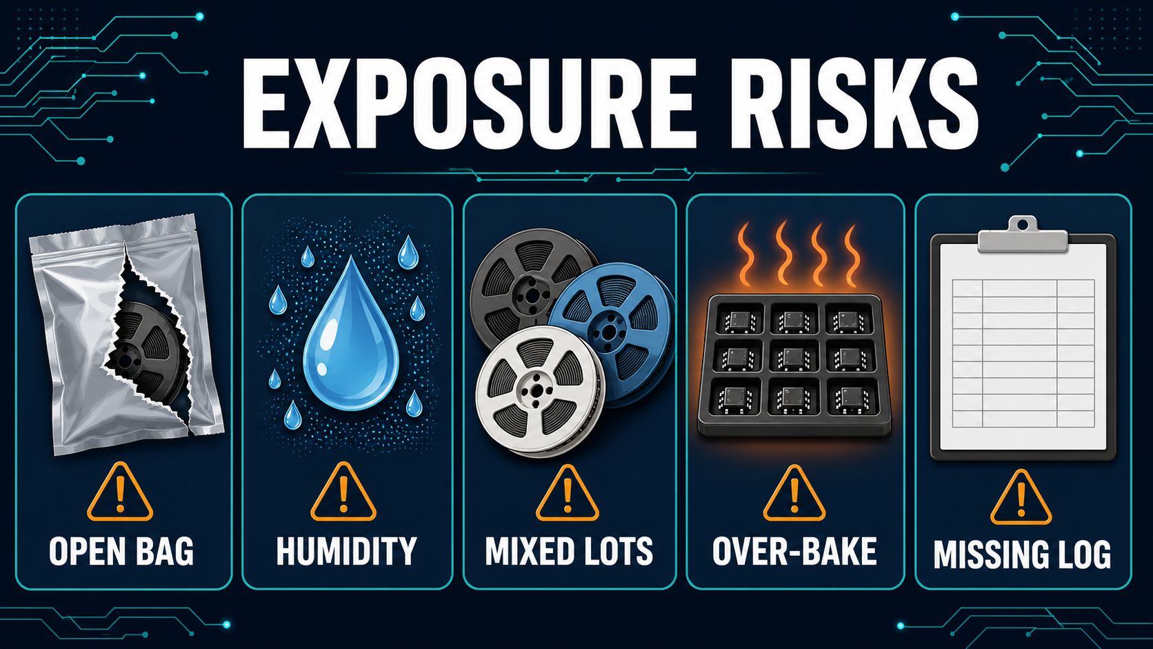
Can EBest Circuit promise a specific laboratory method before review?
No. EBest Circuit can review the package and confirm project-specific support, sample needs, and whether specialized external analysis is required.

You may also like