PCB manufacturing PCB manufacturing
Home > Blog

Custom PCB

Custom PCB Manufacturer for Prototype and Production Builds
Monday, July 20th, 2026
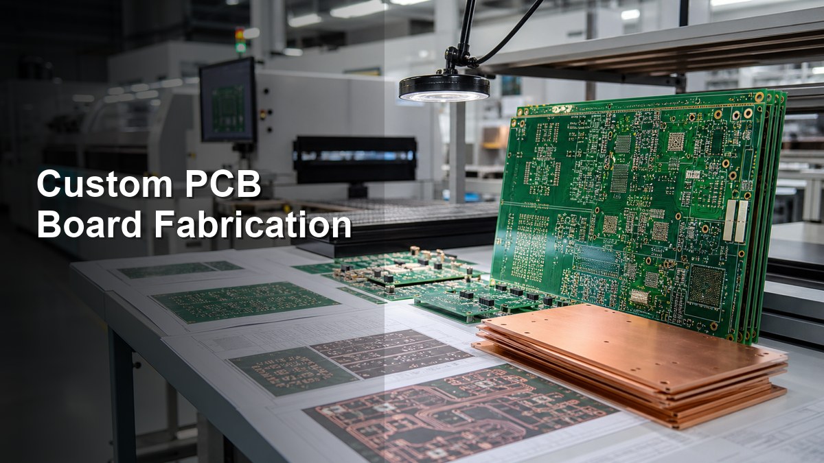
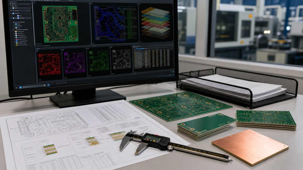
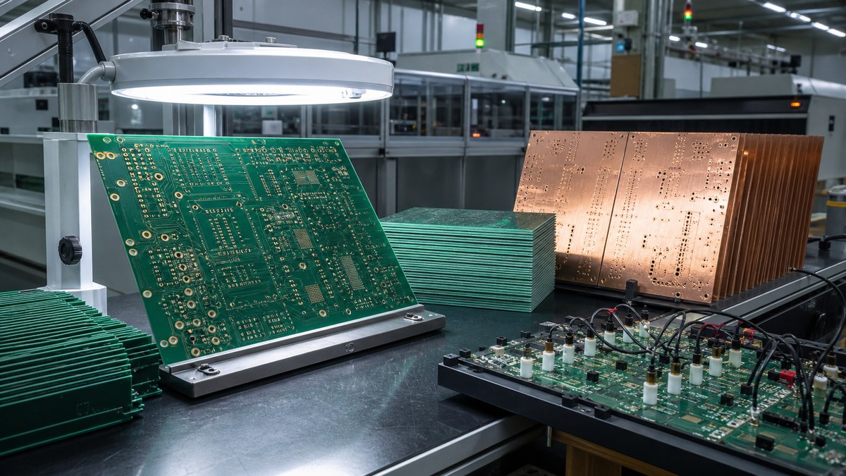
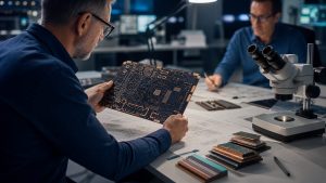
Custom PCB manufacturer engineering review for build-ready circuit boards

A custom PCB manufacturer should do more than make a board from Gerber files. The right partner checks stackup, materials, copper weight, drill data, surface finish, solder mask, panelization, assembly needs, testing requirements and quote assumptions before production starts.

For buyers, the real decision is not simply which factory can produce the lowest unit price. It is whether the manufacturer can turn your design files into reliable boards with the right manufacturing route, clear DFM feedback, stable quality controls and enough support for prototype, small-batch or production orders.

Before choosing a custom PCB manufacturer, check whether your quote package is truly build-ready.

Custom PCB orders often fail at the handoff between design, quotation and production. Buyers should check these risks early:

  • The supplier quotes a standard board even though the design needs special material, controlled impedance, heavy copper, HDI, flex, rigid-flex, metal core or ceramic review.
  • The Gerber, drill, stackup and fabrication drawing do not describe the same board.
  • The quote excludes assembly, BOM review, CPL data, testing, programming, conformal coating or packaging requirements that affect the real project cost.
  • The manufacturer accepts files without flagging spacing, annular ring, solder mask, copper balance, panelization or tolerance risks.
  • The buyer compares suppliers only by unit price and misses quality evidence, communication speed and engineering support.

EBest Circuit supports custom PCB projects with DFM review, manufacturing and optional PCBA coordination.

  • We review Gerber, ODB++, drill files, stackup, fabrication drawings, BOM and CPL files when the project requires a complete PCB or PCBA quotation.
  • We help buyers confirm material, copper, surface finish, board thickness, impedance, solder mask, panelization and testing requirements before production release.
  • We support custom discussions across FR4, HDI, heavy copper, metal core, ceramic, flex and rigid-flex PCB categories when the files need project-specific confirmation.
  • We keep the RFQ discussion focused on build risk, quality controls and realistic project scope instead of only a unit-price comparison.

Custom PCB Manufacturer in One Practical Answer

A custom PCB manufacturer builds boards to project-specific files, materials, dimensions, stackups and quality requirements rather than a fixed catalog design. The manufacturer should review whether the design can be fabricated, assembled, inspected and delivered under the requested conditions.

This article is written for engineers, sourcing teams and product teams comparing custom printed circuit board manufacturers for prototypes, engineering builds, low-volume production or supplier qualification.

When Do You Need a Custom PCB Manufacturer Instead of a Standard PCB Order?

You need a custom PCB manufacturer when the board has requirements that a simple online quote form cannot fully judge. Examples include tight spacing, high layer count, impedance control, unusual thickness, heavy copper, RF laminate, thermal substrate, bend areas, assembly constraints or specific inspection requirements.

If your board is a basic two-layer FR4 prototype, a simple quote tool may be enough. If the board affects heat, signal integrity, fit, vibration, enclosure assembly, compliance documentation or field reliability, the manufacturer should review the files before price becomes the only decision.

What Buyers Should Check Before Sending Files

The best supplier comparison starts with a clean file package and a clear definition of what must be built. A manufacturer cannot quote accurately if the board data, material request, finished thickness, copper weight, surface finish and assembly scope are incomplete or contradictory.

Buyer Check Why It Matters What to Send
Board data Defines the physical circuit Gerber or ODB++, drill, outline and fab notes
Stackup Affects impedance, thickness, lamination and cost Layer order, dielectric targets and copper weight
Material Controls thermal, RF, flex or reliability behavior FR4 grade or special material request
Assembly scope Changes BOM, CPL, stencil, inspection and testing BOM, CPL, assembly drawing and test notes
Acceptance criteria Reduces disputes after delivery IPC class, inspection needs and special notes

How EBest Circuit Supports Custom PCB Manufacturing Projects

EBest Circuit can review custom PCB projects from the manufacturing route through optional PCBA support. The useful starting point is a complete RFQ package, not a vague board description.

For broader capability context, buyers can review EBest Circuit’s PCB manufacturing capabilities. If a project needs assembly, the PCBA and SMT assembly support page helps connect fabrication with component mounting and production planning.

Specifications a Custom PCB Manufacturer Must Confirm

A reliable custom PCB quote should confirm the board specifications that affect manufacturability, cost and risk. At minimum, the discussion should cover layer count, finished thickness, copper weight, minimum trace/space, minimum finished hole, solder mask, silkscreen, surface finish, impedance and panelization.

Some specifications are standard for one factory but special for another. Treat special materials, unusual copper, tight tolerance, HDI, metal core, ceramic, flex or rigid-flex requirements as project-confirmation items rather than assumptions.

Prototype, Small Batch and Production Fit

The right custom PCB manufacturer should match the order stage: prototype, engineering validation, small batch or production. Prototype builds usually prioritize DFM feedback and fast learning, while production builds need stable documentation, repeatable inspection and clear change control.

Buyers should ask whether the quote supports only bare boards or also future assembly, test fixtures, packaging and repeat ordering. A low prototype price can become expensive if the supplier cannot support the next build stage.

Materials, Stackup and Copper Choices

Material, stackup and copper decisions should be confirmed before comparing supplier prices. FR4 remains common for many boards, while special projects may require high Tg FR4, RF laminate, aluminum, copper base, ceramic, flex or rigid-flex structures.

For FR4-related project planning, see EBest Circuit’s FR4 PCB material options. For any special material or tight process requirement, the safest wording is project confirmation: send the files and ask the manufacturer to verify whether the requested construction is standard, special or not recommended.

DFM Review Before Custom PCB Fabrication

DFM review catches manufacturing risk before CAM release, procurement and production scheduling. It should check spacing, annular ring, drill aspect ratio, copper balance, solder mask bridge, silkscreen clearance, board outline, panel rail, fiducials and test access.

A good DFM review does not replace the engineer’s design responsibility. It helps identify file conflicts and production risks early enough to revise the layout, change a material assumption or clarify a tolerance before the order is released. For a connected view of design release and production planning, see the PCB design and manufacturing workflow.
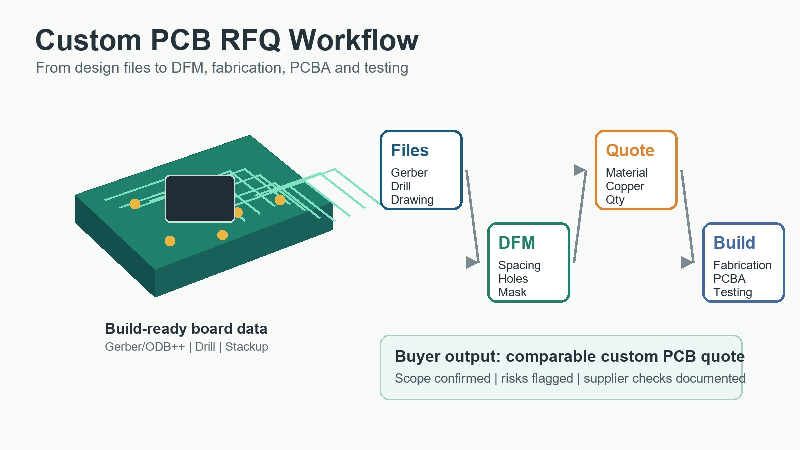
Custom PCB RFQ workflow from design files to DFM review manufacturing PCBA and testing

PCBA, BOM and Component Sourcing Support

If the finished product needs assembly, the custom PCB quote should include PCBA assumptions early. Bare-board fabrication and assembly are connected by pad design, solder mask, stencil openings, component availability, CPL accuracy, inspection method and test requirements.

When a project includes assembly, ask the manufacturer to review BOM, CPL, assembly drawing, polarity notes, special components, programming and functional test expectations together with the bare board files.

Quality, Inspection and Testing Evidence

Quality evidence matters more than broad claims such as “high quality” or “best manufacturer.” Ask what inspection steps apply to your board type: electrical test, AOI, X-ray for hidden solder joints, impedance report, first article review, final visual inspection or functional test when the project requires it.

The exact evidence should match the order. A simple bare board does not need the same proof package as a high-density assembly, and a prototype may need different documentation than a repeat production run.

Cost Drivers in a Custom PCB Quote

Custom PCB cost changes when the design requires more material control, process complexity, inspection effort or assembly coordination. Main drivers include layer count, board size, material, copper weight, minimum trace/space, finished hole size, surface finish, impedance, routing, quantity, testing and PCBA scope.

Do not compare suppliers only by the first quoted unit price. Compare what is included, what is excluded, what requires engineering confirmation and what happens if files need revision after DFM review.

For cost-focused buying checks, use the cheap PCB manufacturing cost and quality checklist as a companion reference. If the project is still in first-article validation, the prototype PCB manufacturing RFQ guide helps connect early builds with future production assumptions.

RFQ File Checklist for Custom PCB Manufacturing

A complete RFQ package reduces quote delay and prevents mismatched assumptions. Send the manufacturer enough information to identify the board, build route, inspection needs and commercial scope.

  • Gerber or ODB++ files and NC drill data.
  • Fabrication drawing with board thickness, copper, finish, tolerance and notes.
  • Stackup and impedance targets when required.
  • Quantity, target date and prototype or production stage.
  • BOM, CPL, assembly drawing and test plan if PCBA is included.
  • Special material, thermal, high-current, flex, rigid-flex, ceramic or metal-core requirements.

Red Flags When Comparing Custom PCB Manufacturers

Supplier red flags usually appear before production if buyers ask the right questions. Be careful when a manufacturer quotes without checking files, gives a very low price with unclear exclusions, avoids DFM discussion, cannot explain inspection steps or pushes all responsibility back to the buyer after file upload.

Price, speed, location and past supplier experience are useful comparison points, but the final decision should still depend on the board’s engineering risk and the supplier’s ability to support your exact build.

Questions to Ask Before You Approve a Supplier

The final supplier decision should be based on build fit, evidence and communication clarity. Before approving a custom PCB manufacturer, ask direct questions that reveal whether the supplier understands your project.

  1. Which specifications are standard, special or need engineering confirmation?
  2. What DFM issues should be corrected before production?
  3. Which material, copper and surface finish options fit the application?
  4. What inspection or test evidence will be supplied?
  5. Does the quote include only bare boards, or also assembly, BOM review and testing?
  6. What information is still missing from the RFQ package?

Custom PCB Manufacturer FAQ

What is a custom PCB manufacturer?
A custom PCB manufacturer builds printed circuit boards from project-specific design files, materials, dimensions, stackups and production requirements. The supplier should confirm manufacturability before fabrication.

Is a custom PCB manufacturer different from a PCB maker?
Sometimes the terms overlap. In buying decisions, a custom PCB manufacturer usually implies stronger file review, process confirmation, material choice, quality control and project support than a simple hobby PCB maker.

What files are needed for a custom PCB quote?
Send Gerber or ODB++, NC drill, fabrication drawing, stackup, quantity and special requirements. For assembly, also send BOM, CPL, assembly drawing, test notes and programming requirements if applicable.

Can a custom PCB manufacturer also assemble the board?
Some manufacturers can coordinate PCBA, while others only fabricate bare boards. Confirm BOM review, CPL review, SMT, through-hole, inspection and testing scope before comparing quotes.

Final Recommendation

Choose a custom PCB manufacturer that can prove fit for your board, not just quote the lowest price. The strongest RFQ process starts with complete files, clear specifications, DFM review, quality evidence and a supplier that can support the project stage you are actually building.

Send your Gerber or ODB++, drill files, stackup, fabrication drawing, quantity, target schedule and BOM/CPL if assembly is needed to sales@bestpcbs.com. EBest Circuit can review your custom PCB manufacturing requirements and provide a practical quotation path for bare boards, PCBA or build-ready projects.

You may also like

Custom PCB Manufacturer Selection and RFQ Guide
Wednesday, July 15th, 2026
Custom PCB manufacturer RFQ guide with engineer reviewing circuit boards

A custom PCB manufacturer should be chosen by file review quality, build capability, assembly scope, testing plan, communication and quote transparency, not only by the lowest instant price. The current supplier comparison landscape show that buyers are comparing online prototype suppliers, PCB fabrication companies, assembly providers and forum recommendations before ordering.

This guide helps engineers and purchasing teams compare custom PCB manufacturing options, prepare RFQ files and decide when bestpcbs is a practical supplier for prototypes, low-volume builds, special materials or PCB assembly.

Custom PCB Manufacturer at a Glance

A custom PCB manufacturer turns project-specific Gerber or ODB++ data into fabricated circuit boards, and may also support assembly, component sourcing, testing and production planning. The useful buying question is whether the supplier can review your actual project risk before production starts.

Buyer question What to check Why it matters
Can they build the board? Layer count, material, copper, drill, finish and special process fit Custom PCB work depends on the actual stackup and feature limits.
Can they review the files? DFM feedback, missing notes and quote assumptions Prevents avoidable fabrication holds.
Is assembly included? BOM, CPL, component sourcing, inspection and test scope PCBA risk is often larger than bare-board risk.
Is the quote comparable? Same files, same finish, same test, same freight and same lead-time assumptions Different quote scopes make price comparisons misleading.

Customer Pain Points in Custom PCB Manufacturing Projects

Custom PCB projects often fail at the handoff between design intent and manufacturing reality, so the supplier must help clarify files, materials, tolerances, assembly scope and inspection expectations before production.

Customer Pain Point Project Risk How bestpcbs Helps
The Gerber or ODB++ package is released, but stackup, material or copper requirements are still incomplete. The quote may look acceptable while the real build requirement remains undefined. bestpcbs requests fabrication data, stackup notes, material, copper, finish and quantity together so engineering review can catch missing assumptions early.
The project needs both PCB fabrication and assembly, but BOM and placement data are not checked together. Component risk, footprint mismatch or assembly constraints may appear after boards are already made. bestpcbs can review PCB files with BOM and CPL when PCBA is required, helping buyers connect fabrication and assembly decisions before release.
Special requirements such as impedance, HDI, flex, rigid-flex, metal core, ceramic or heavy copper are not described clearly. The supplier may quote a standard board even though the design needs a controlled process route. bestpcbs asks buyers to call out special process, material, test and documentation needs so the quote can reflect the actual project risk.
The buyer wants a low price, but also needs fewer engineering surprises. Missing DFM checks can lead to redesign, delay, scrap or unexpected cost later. bestpcbs positions the RFQ around DFM review, manufacturability questions and acceptance requirements, not only unit price.

Custom PCB Buyer Priorities Before Quote

Custom PCB buyers should define the board structure, material, finish, tolerance, assembly scope and testing needs before comparing suppliers. A custom quote is only useful when each supplier is pricing the same requirements.

Prepare Gerber or ODB++ files, drill data, drawings, BOM, CPL, quantities and application notes. A supplier that reviews these files early can help identify missing details before cost, lead time or manufacturing risk becomes locked in.

When This Custom PCB Manufacturer Guide Fits

This guide fits buyers who need more than a commodity two-layer prototype order. It is especially useful when the design has controlled impedance, HDI, rigid-flex, high current, metal core, ceramic, RF, assembly or testing requirements that an instant calculator may not fully evaluate.

If the project is a broad supplier search, the existing custom PCB supplier page is a useful companion. This article focuses more narrowly on manufacturer selection and RFQ preparation.

Prototype, Low-Volume and Production Options

Prototype, low-volume and production PCB orders should be compared separately because each stage has a different risk profile. A supplier that is convenient for a first prototype may not be the right production partner if assembly, testing, revision control or special process support becomes important.

Project stage Main buyer need Supplier check
Prototype Fast learning and file validation DFM review, material availability and revision feedback.
Low volume Stable process before scaling Repeatability, inspection, assembly data and cost assumptions.
Production Yield, traceability and supply continuity Process control, test plan, packaging and forecast support.
custom pcb manufacturer RFQ checklist for supplier review
custom pcb manufacturer RFQ checklist for supplier review.
custom pcb manufacturer risk review flow before production
custom pcb manufacturer risk review flow before production.

For prototype-specific preparation, see the prototype PCB manufacturing RFQ checklist.

PCB Types and Materials to Confirm

Custom PCB manufacturing becomes risky when the RFQ does not clearly state the board type, material and process assumptions. Buyers should tell the manufacturer what the board must do, not only send files and ask for price.

  • FR4, high Tg, Rogers or other high-frequency material.
  • Single-sided, double-sided, multilayer, HDI or rigid-flex structure.
  • Heavy copper, metal core, ceramic or other special construction.
  • Controlled impedance, plated slots, blind/buried vias or fine pitch features.
  • Surface finish, solder mask color, board thickness and copper weight.

For deeper capability context, the PCB fabrication manufacturer selection guide and multi-layer PCB page are relevant internal references.

DFM Review Before Custom PCB Manufacturing

DFM review is the point where a custom PCB manufacturer proves whether it is only taking an order or actually reducing manufacturing risk. A good review should flag unclear notes, missing drill data, tight spacing, stackup conflicts, panelization issues, solder mask problems and assembly access concerns.

  • Check minimum trace and spacing against copper and process needs.
  • Review drill size, annular ring, slots, cutouts and board outline.
  • Confirm stackup, dielectric, impedance and controlled layer order.
  • Review panelization, fiducials and tooling holes if assembly is needed.
  • Confirm solder mask openings, silkscreen readability and polarity marks.
  • Identify which questions must be answered before production release.

PCB Assembly and Component Sourcing Scope

If the project needs PCBA, evaluate the manufacturer as a fabrication and assembly partner, not only as a bare-board supplier. Assembly introduces BOM risk, package mix, component sourcing, soldering profile, polarity, inspection and test requirements.

Bestpcbs can support PCBA and PCB assembly service together with board fabrication. Send BOM, CPL, assembly drawing, substitute rules and test requirements with the Gerber package so the assembly review happens early.

Testing and Quality Control Questions

Testing requirements should be defined before ordering because a low quote may include fewer checks than the project actually needs. Custom PCB quality is not only about whether the board powers on; it is about whether the board matches the design and can be repeated.

Quality item What to ask Why it matters
Bare-board electrical test Is continuity and isolation testing included? Confirms the fabricated board matches the netlist.
Impedance report Is controlled impedance verified when required? Critical for high-speed and RF designs.
Assembly inspection Will AOI, X-ray or functional checks be used? Depends on component package and risk.
Traceability How are revisions, lots and component substitutions controlled? Important for repeat orders and field support.

What Determines Custom PCB Manufacturing Cost?

Custom PCB cost is driven by board complexity, material, copper, surface finish, minimum features, testing, assembly scope, quantity, lead time and the completeness of the RFQ package. A cheap online price can change once missing requirements are added.

Use the custom PCB cost guide to compare quote drivers in more detail. For supplier selection, make sure each manufacturer is pricing the same board, same files, same tests and same shipping assumptions.

How to Compare Custom PCB Manufacturers

Compare custom PCB manufacturers by the questions they ask, the assumptions they document and the risks they help remove before production. Price still matters, but it should be compared after the scope is aligned.

  • Do they support the required board type and material?
  • Do they perform DFM review before release?
  • Can they quote fabrication and assembly together when needed?
  • Do they explain test, inspection and reporting assumptions?
  • Can they handle prototype, low-volume and repeat production stages?
  • Do they avoid unsupported promises about universal lead time or yield?

Quote Files to Prepare Before Contacting a Manufacturer

A complete RFQ package lets a custom PCB manufacturer quote the real project instead of guessing from partial design files. This is the easiest way to reduce delays and false quote comparisons.

  • Gerber or ODB++ fabrication files and drill files.
  • Stackup, material, copper, thickness and surface finish notes.
  • Mechanical drawing for outline, slots, cutouts and critical dimensions.
  • Controlled impedance requirements and special process notes.
  • BOM, CPL and assembly drawing if PCBA is required.
  • Testing, inspection, packaging and labeling requirements.
  • Quantity, revision, project stage and target lead time.

Common Custom PCB Sourcing Risks

The most common sourcing risk is comparing manufacturers before the project scope is clear. That creates hidden differences in material, test coverage, assembly ownership, freight, lead time and revision control.

  • Do not compare a bare-board quote with a turnkey PCBA quote.
  • Do not assume instant online pricing includes every special process.
  • Do not leave controlled impedance, testing or surface finish unclear.
  • Do not wait until after the order to send BOM and CPL for assembly.
  • Do not choose a supplier only because a forum recommends them for a different board type.

Frequently Asked Questions About Custom PCB Manufacturers

What is a custom PCB manufacturer?

A custom PCB manufacturer fabricates printed circuit boards from project-specific design files rather than selling a fixed standard board. The manufacturer may support prototypes, production boards, special materials, DFM review, assembly and testing depending on the project.

How do I choose a custom PCB manufacturer?

Choose by matching the supplier’s capability to your board type, material, stackup, assembly scope, testing needs and delivery plan. Then compare price after every supplier is quoting the same files and requirements.

Can one supplier handle both custom PCB fabrication and assembly?

Yes, if the supplier supports both fabrication and PCBA. A combined path can reduce handoff errors because Gerber or ODB++, BOM, CPL, assembly drawings and test notes can be reviewed together.

What should I send for a custom PCB quote?

Send Gerber or ODB++, drill files, stackup notes, material and finish requirements, quantity, mechanical drawings, testing requirements and target lead time. For assembly, also send BOM, CPL and assembly drawings.

Final RFQ Recommendation

Before choosing a custom PCB manufacturer, align the files, scope and acceptance criteria so every quote is based on the same project. This matters more than collecting many fast prices that do not include the same assumptions.

For a custom PCB quote, send Gerber or ODB++ files, drill data, stackup, material, copper, surface finish, mechanical drawings, BOM, CPL, assembly drawings, testing requirements, quantity and target lead time to sales@bestpcbs.com. Best Technology / bestpcbs can review the package, confirm which items need DFM or process checking and help compare the project as prototype fabrication, PCBA, low-volume production or a repeat manufacturing RFQ.

You may also like

Custom PCB Design for Sensors: Signal, Power and Test Checks
Monday, July 13th, 2026
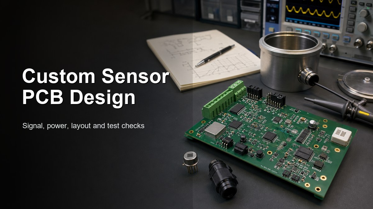
Custom sensor PCB design workbench with sensor board, oscilloscope and enclosure parts

Custom PCB design for sensors should be reviewed around signal accuracy, low-noise power, grounding, connector placement, calibration access, test points, environmental protection and production-ready RFQ files. A sensor PCB is not only a small carrier board for a sensing element. It is the interface between the real world and the electronics that must read that signal consistently.

This guide is written for engineers and buyers preparing a custom sensor PCB or sensor PCBA for industrial devices, IoT products, environmental monitoring, equipment controls, medical-adjacent instruments, automotive modules or field equipment. It focuses on manufacturable board design and supplier review, not on selecting one specific sensor IC.

What does custom PCB design for sensors need to solve?

A sensor PCB needs to preserve the signal the sensor produces while surviving the mechanical, electrical and environmental conditions around the final product. The board may measure temperature, pressure, humidity, light, motion, gas, current, position or vibration, but the design checks follow a similar pattern: protect the signal path, control noise, provide stable power and make the board testable.

Low-current analog sensors may need guarded routing, short high-impedance traces and careful leakage control. Digital sensors may need clean I2C, SPI, UART, CAN, RS-485 or wireless module routing. Compact sensor products may use an HDI PCB when the enclosure is tight and the connector, MCU, RF section and sensing element compete for space.

Sensor board area PCB design check Buyer or engineer risk
Signal path Short routing, shielding, filtering, impedance or guard traces when needed Noise, drift or unstable readings can hide the real sensor output
Power supply Low-ripple rails, local decoupling, regulator heat and startup behavior Power noise can show up as false measurement changes
Grounding Analog/digital return paths, chassis connection and cable shield plan Ground loops or poor return paths can create hard-to-debug faults
Environment Coating, enclosure interface, sensor exposure window and connector sealing Humidity, dust, chemicals or vibration can change readings or damage the board
Production test Test pads, calibration points, programming access and fixture clearance Good prototypes can become slow or inconsistent in volume builds

Which sensor applications need a custom PCB?

A custom PCB is useful when the sensor board must fit a product enclosure, meet a specific noise target, connect to a harness, support calibration or survive a defined operating environment. Evaluation boards are useful for early testing, but they rarely match the size, connector, grounding, power and protection requirements of the final product.

Common examples include environmental sensor nodes, industrial monitoring modules, battery and charger sensors, flow meters, load-cell interfaces, motor feedback boards, optical sensor boards, wearable sensor modules and equipment health monitoring electronics. Many designs can use an FR4 Printed Circuit Board. High-frequency, wireless or antenna-connected sensor products may need RF material decisions, controlled routing or a review against an RF PCB capability page.

How should low-noise layout be planned?

Low-noise sensor layout starts with floorplanning: keep the sensor front end, reference, ADC, filter, connector and noisy switching circuits in controlled zones. A layout can pass a simple connectivity check but still produce unstable data if switching regulators, antennas, motors, relays or long cable inputs couple noise into the measurement path.

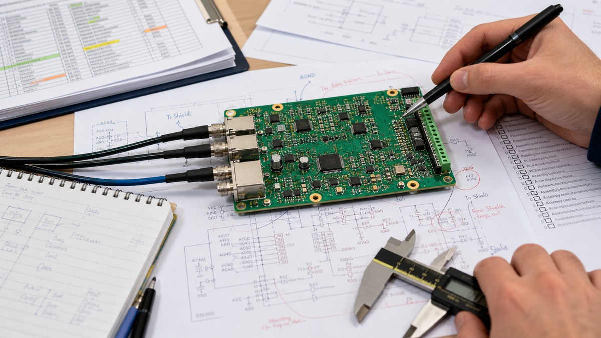
Custom sensor PCB DFM review with schematic, connector cables and layout notes
Sensor PCB design should be reviewed as a complete signal chain, not only as a component placement task.

Place the sensor and analog front end close together when the signal is small. Keep high-current switching loops away from sensitive inputs. Use a continuous reference plane where possible, and avoid splitting a return path under critical traces without a clear reason. For cable-connected sensors, review ESD, surge, filtering and shield termination before release. If the design uses a flex tail or adhesive-mounted sensing element, confirm bend area, stiffener position and assembly handling early.

What power and grounding checks matter most?

Power and grounding checks should answer whether the sensor reading stays stable during startup, load changes, communication bursts and nearby switching events. Sensors that look accurate on a bench supply can become noisy when they share power with radios, relays, motors, LEDs, heaters or long cable harnesses.

Ask the designer or supplier to review regulator choice, decoupling placement, reference voltage routing, ground return, cable shield strategy and any required isolation. If a sensor board includes both sensitive analog inputs and digital communication, the layout should support both signal integrity and production assembly. When the order includes SMT, through-hole parts, connectors and final inspection, discuss the project as a Prototype PCB Assembly or production PCBA job instead of a bare PCB only.

How should connectors, cables and enclosures be designed?

Sensor PCB reliability often depends on connector orientation, cable strain relief, enclosure clearance and how the sensor is exposed to the measured environment. A board can be electrically correct but hard to assemble if the cable exits the wrong side, the sensor window does not align, or the test pads are blocked by the housing.

Before fabrication, compare the PCB outline with the enclosure model, mounting bosses, gasket, sensor opening, cable routing and service access. For field devices, define whether the board needs conformal coating, potting, a vented enclosure, connector sealing or a separate daughterboard. If the supplier is expected to assemble the PCB into a housing or harness, treat the RFQ as a Box Build Assembly discussion.

When do flex or rigid-flex sensor boards make sense?

Flex and rigid-flex sensor boards make sense when the sensing element must sit away from the main electronics, bend around a shape, reduce connector count or fit a compact enclosure. They are common in wearables, medical-adjacent devices, compact industrial sensors, optical modules, probes and adhesive-mounted sensing assemblies.

Flex is not a shortcut around mechanical design. Bend radius, copper direction, stiffener location, adhesive choice, strain relief and assembly sequence still need review. If a sensor product uses a flexible circuit, compare the design against a proven custom flex PCB design checklist before ordering production tooling.

What should be included in the sensor PCB test plan?

The test plan should prove that the board can be fabricated, assembled, programmed, calibrated and checked repeatedly before it reaches the final product. For sensor PCBA, continuity alone is usually not enough. The test may need known input conditions, reference measurements, firmware loading, communication checks and pass/fail limits.

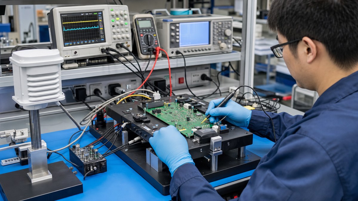
Sensor PCBA functional testing with oscilloscope, test fixture and environmental sensor enclosure
Plan functional test and calibration access before the board is released for production.

Add test pads for power rails, ground, programming, communication lines and critical analog nodes. Keep them reachable after assembly and enclosure installation. If calibration is needed, define the calibration input, equipment, firmware state and acceptable tolerance. A supplier’s PCB test equipment and fixture planning should be discussed before volume production, not after failed boards appear.

RFQ checklist for custom sensor PCB design

A strong RFQ package lets the supplier review sensor accuracy, manufacturability, assembly risk and test coverage before quoting price and lead time. Send controlled files instead of screenshots or partial exports.

  1. Gerber files, drill files, netlist and controlled revision number.
  2. Schematic, stackup, copper weight, board thickness and surface finish requirement.
  3. Sensor type, expected signal range, accuracy goal and calibration requirement.
  4. Power input range, current load, regulator notes and any battery or charger interface.
  5. Connector, cable, enclosure, coating, potting or gasket information.
  6. BOM, approved alternates, centroid file and assembly drawing for PCBA.
  7. Programming method, firmware loading requirement and functional test criteria.
  8. Environmental notes such as temperature, humidity, vibration, dust, chemicals or outdoor exposure.

Supplier questions buyers should ask

The best supplier questions force a real DFM and test review instead of a generic board price. Use them before approving the first build.

  • Which parts of this sensor design create the highest layout or assembly risk?
  • Are the sensor, connector and enclosure clearances consistent with the mechanical file?
  • Do any analog inputs need additional spacing, guarding, shielding or cleaning controls?
  • Are the test pads reachable after assembly and enclosure installation?
  • Which components have sourcing risk or need approved alternates?
  • Can the test fixture simulate or verify the sensor input reliably?
  • What should change before moving from prototype to pilot production?

Sensor boards often depend on stable parts. If a project uses specialized sensor ICs, connectors, filters, references or wireless modules, involve Component Sourcing early so substitutes do not change measurement behavior without engineering approval.

FAQ

What is custom PCB design for sensors?

Custom PCB design for sensors means designing a circuit board around a sensing element, signal chain, power system, connectors, firmware access and test plan for a specific product. The goal is to read the sensor accurately and build the board repeatedly, not just connect a sensor IC to a controller.

Does every sensor PCB need a four-layer board?

No. Simple low-speed digital sensor boards may work on two layers when routing, power and grounding are clean. Mixed-signal, wireless, compact or low-noise sensor boards often benefit from four or more layers because a stable reference plane and controlled return paths reduce layout risk.

What causes noise in sensor PCB readings?

Common causes include unstable power rails, poor grounding, long high-impedance traces, switching regulator noise, nearby motors or relays, cable pickup, weak shielding, poor filtering and bad test setup. The fix depends on the sensor type and signal level, so schematic and layout review should happen before fabrication.

What files are needed for a sensor PCB quote?

Send Gerber and drill files, schematic, stackup, board drawing, BOM, centroid file, assembly drawing, enclosure notes and test requirements. If calibration, coating, potting, firmware loading or box build is required, include those details in the first RFQ.

Can a PCB supplier improve sensor accuracy?

A PCB supplier can help with manufacturability, material choice, assembly quality, inspection and repeatable testing. Accuracy still depends on the sensor IC, circuit design, layout, calibration method, firmware and operating environment. Treat supplier feedback as one part of the engineering review.

Conclusion

Custom PCB design for sensors should start with the measurement problem, not with board price. Define the signal, power rails, grounding, enclosure, connector, calibration and test plan before production files are released. Then ask the supplier to review manufacturability and assembly risk against the real use case. That process gives the sensor board a better chance of producing stable readings in the final product.

You may also like

Custom PCB Board Fabrication
Sunday, July 12th, 2026
Custom PCB board fabrication with circuit boards, copper panels and manufacturing documents
Custom PCB board fabrication works best when the supplier can review the design intent, materials, stackup and inspection needs before production starts.

Custom PCB board fabrication is the process of turning production-ready design data into a physical printed circuit board built to a specific stackup, material, copper weight, surface finish, tolerance and inspection requirement. A reliable fabrication order is not defined only by board size or layer count. It depends on clean Gerber or ODB++ data, drill files, material availability, manufacturable design rules, controlled process steps and clear acceptance criteria.

For engineers and buyers, the most useful question is not simply “who can make a custom PCB?” The better question is “what information does the fabricator need to build this board correctly the first time?” This guide explains the file package, material decisions, fabrication steps, inspection checks and supplier questions that matter before RFQ.

What Is Custom PCB Board Fabrication?

Custom PCB board fabrication means manufacturing a bare PCB from a customer-specific design rather than buying a standard off-the-shelf board.

The design may be a simple two-layer FR4 board, a dense multilayer board, an HDI board, a heavy copper power board, a metal-core board, a ceramic substrate, or another application-specific construction. The fabricator prepares production tooling from the supplied data, images the copper layers, drills holes, plates vias, applies solder mask and legend, adds the chosen surface finish, routes or scores the outline, and tests the board before shipment.

A custom board gives the designer control over shape, connector position, layer structure, impedance, copper width, heat path, mounting holes and assembly fit. That control also creates responsibility: unclear design notes, missing drill files or unrealistic tolerances can delay production or create boards that are technically built but not suitable for the final product.

Files Needed Before a PCB Can Be Fabricated

A fabricator can only confirm price, lead time and manufacturability when the production file package describes the board without guessing.

For bare PCB fabrication, send Gerber or ODB++ files, NC drill files, board outline, layer stackup, copper weight, finished thickness, material requirement, solder mask color, legend color, surface finish, impedance notes, controlled-depth drilling notes, special plating requirements and a fabrication drawing if tolerances matter. If the board will later be assembled, include the BOM, centroid file and assembly drawing early so the bare board can support the assembly process.

PCB fabrication file review with CAM layers, drill drawing, sample boards and calipers
File review should catch stackup, drill, outline, material and tolerance issues before the board enters production.

Common file problems include an outline that does not match the mechanical drawing, plated and non-plated holes mixed in one unclear drill file, missing impedance information, no material callout, ambiguous copper weight, or a solder mask opening that conflicts with fine-pitch parts. These problems are easier to fix before fabrication than after panels are released to production.

Material and Stackup Choices That Change Fabrication Risk

Material and stackup decisions control cost, lead time, yield and long-term reliability more than many buyers expect.

Standard FR4 printed circuit board builds are usually easier to quote and schedule than special laminates. However, high Tg FR4, RF material, ceramic substrate, metal-core construction, rigid-flex material and heavy copper boards may be necessary for temperature, power, frequency or mechanical requirements. The right material should be chosen for the operating environment, not only for the lowest unit price.

Stackup also matters. Controlled impedance, sequential lamination, buried vias, blind vias, via-in-pad, thin dielectric spacing and unusual finished thickness can all add manufacturing checks. If the design needs high wiring density, compare the layout against realistic HDI PCB process limits before asking for fast delivery.

Typical PCB Fabrication Steps Buyers Should Understand

The fabrication process is a controlled chain of imaging, drilling, plating, finishing and testing steps, so a weak early decision can affect the final board.

Stage What Happens Buyer Check
CAM and DFM review Files are checked for manufacturability, layer alignment, drill data, spacing and special notes. Confirm all design files match the intended revision.
Material preparation Copper-clad laminate, prepreg, copper foil and special materials are prepared. Verify material grade, board thickness and copper weight.
Inner and outer layer imaging Copper patterns are transferred and etched according to the design data. Check fine line and spacing against supplier capability.
Drilling and plating Mechanical or laser holes are drilled, then plated to connect layers. Review hole size, annular ring and aspect ratio risk.
Solder mask and surface finish Solder mask, legend and finish such as HASL, ENIG, OSP or immersion silver are applied. Select a finish that fits component type, shelf life and assembly method.
Profiling and testing Boards are routed, V-scored, electrically tested and inspected before packing. Define acceptance criteria and required reports before production.

For a broader process reference, Best Technology’s PCB manufacturing page shows how raw material preparation, lamination, drilling, plating, solder mask, testing and packing fit together in a complete bare-board flow.

This PCB process video is used as a visual supplement only; the checklist above should still be reviewed in text before RFQ.

Design Rules That Should Be Checked Before RFQ

DFM review should focus on the few design limits that can change yield, price or delivery before the buyer approves production.

  • Minimum trace width and spacing for the chosen copper weight.
  • Minimum mechanical drill, laser drill and finished hole size.
  • Annular ring, drill-to-copper clearance and edge-to-copper clearance.
  • Aspect ratio for plated through holes and microvia structure for HDI boards.
  • Solder mask bridge width for fine-pitch components.
  • Controlled impedance stackup, dielectric thickness and copper roughness assumptions.
  • Panelization, V-score or routing needs for assembly handling.
  • Surface finish compatibility with BGA, fine pitch, wire bonding or storage conditions.

If the project includes SMT, through-hole assembly or turnkey sourcing, bare board fabrication should be planned with PCB assembly support in mind. Pad design, fiducials, panel rails, solder mask openings and test points can make assembly easier or create avoidable rework.

Inspection and Testing Should Be Defined Early

Inspection should match the risk level of the board, not a generic checklist copied from another project.

Typical checks include visual inspection, dimensional measurement, solder mask inspection, electrical open/short testing, impedance coupon testing when specified, microsection review for high-reliability builds, and final packing inspection. For boards used in power electronics, automotive equipment, medical devices, aerospace-related hardware or outdoor products, buyers should define the required standard, report format and acceptance level before quotation.

PCB fabrication inspection with finished circuit boards, copper panels and test fixture equipment
Electrical testing, visual inspection and process records help confirm that the fabricated boards match the approved design data.

Quality checks are also practical supplier filters. A fabricator that can explain test equipment, inspection points and process records is usually easier to work with than one that only quotes a low price. Best Technology’s PCB test equipment page is a useful internal reference when a buyer wants to understand what inspection capability may be relevant.

Cost and Lead Time Factors in Custom PCB Fabrication

Custom PCB fabrication cost and lead time usually increase when the board needs more controlled process steps or less common material.

Important cost drivers include layer count, panel utilization, board thickness, copper weight, line width and spacing, hole count, smallest drill, blind or buried vias, surface finish, impedance control, special material, testing requirements, quantity and delivery speed. A small board is not always cheap if it requires HDI, heavy copper, tight drilling or special laminate. A larger board may be easier if it uses standard material and relaxed tolerances.

Buyers should ask suppliers to separate tooling, bare board fabrication, assembly, component sourcing, testing and shipping costs when the project includes more than the bare PCB. This prevents a low board price from hiding a high assembly or logistics risk.

Supplier Questions Before You Approve Fabrication

The best RFQ questions help the supplier expose manufacturing risk before the board enters production.

  • Are any traces, spaces, holes or annular rings outside standard capability?
  • Is the requested material in stock, or does it require special sourcing?
  • Does the stackup support the required impedance and finished thickness?
  • Is the selected surface finish suitable for the component packages and storage time?
  • Are there any panelization issues that could affect assembly or depaneling?
  • Which tests are included, and which reports require an extra request?
  • What design change would reduce cost, lead time or yield risk?

If the design falls outside standard FR4 or routine multilayer production, a special PCB review can help clarify whether the project needs heavy copper, high-frequency material, metal core, ceramic, rigid-flex or another custom process path.

FAQ

What files are required for custom PCB board fabrication?

Most fabrication orders need Gerber or ODB++ files, NC drill files, board outline, stackup, copper weight, thickness, material, solder mask, legend, surface finish and any special tolerance notes. A fabrication drawing is useful when dimensions, impedance, controlled-depth drilling or acceptance criteria matter.

Is PCB fabrication the same as PCB assembly?

No. PCB fabrication makes the bare printed circuit board. PCB assembly places and solders components onto that board. A turnkey PCBA project needs both steps, plus BOM review, component sourcing, stencil planning, inspection and testing.

What makes a custom PCB harder to fabricate?

HDI microvias, blind or buried vias, heavy copper, tight spacing, unusual thickness, special materials, controlled impedance, fine-pitch solder mask, large panels and strict inspection requirements can all increase fabrication difficulty.

Which surface finish should I choose?

The right finish depends on assembly method, component package, shelf life, flatness and cost. ENIG is often chosen for fine pitch and flatness, HASL can fit less demanding boards, and OSP may fit some cost-sensitive builds. Confirm with the assembler before ordering.

How can I reduce PCB fabrication cost?

Use standard material when possible, improve panel utilization, avoid unnecessary tight tolerances, simplify via structures, keep copper weight realistic, choose a suitable finish and send complete files. Do not remove inspection that protects product reliability.

Can a fabricator fix my PCB design files?

A fabricator can often flag manufacturability issues and suggest changes, but it should not silently change electrical intent. Any change to spacing, pad shape, drill size, stackup or material should be reviewed and approved by the design owner.

When should I request impedance control?

Request impedance control when the board carries high-speed digital, RF, differential pairs, antennas or other signals that depend on trace geometry and dielectric structure. Provide target impedance, tolerance, reference layers and stackup requirements.

Does custom PCB fabrication always take longer than standard PCB orders?

Not always. A custom board with standard FR4, clean files and routine tolerances can move quickly. Lead time increases when the design needs special material, complex stackup, extra testing, unusual finish or unresolved DFM clarification.

Final Thoughts

Custom PCB board fabrication is predictable when the design files, stackup, material choices, process limits and inspection requirements are clear before production. The safest RFQ is not the one with the fewest details. It is the one that lets the supplier identify cost, lead time and yield risk before the first panel is built.

If you are preparing a custom PCB for prototype or production, send your Gerber, drill, stackup, BOM and assembly files to the Best Technology engineering team at sales@bestpcbs.com for fabrication, PCBA and quotation review.

You may also like

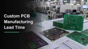
Custom PCB Manufacturing Lead Time
Saturday, July 11th, 2026
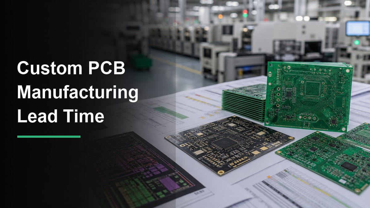
Custom PCB manufacturing lead time planning with PCB boards and production documents
Custom PCB lead time is easier to control when design files, materials, production steps and inspection needs are reviewed before quotation.

Custom PCB manufacturing lead time is the time from approved production files and quote confirmation to finished boards or assembled PCBAs ready for shipment. It is not set only by layer count. File quality, material availability, surface finish, copper weight, impedance control, component sourcing, testing scope, production queue and shipping route can all add or remove days.

For buyers, the practical question is not “what is the fastest possible PCB lead time?” The better question is “what information does the factory need to confirm a reliable lead time for this exact board?” A simple FR4 prototype with complete Gerbers can move quickly. A custom PCB with HDI, controlled impedance, special laminate, heavy copper, tight drilling, turnkey assembly or functional testing needs a more careful schedule.

What Counts as Custom PCB Manufacturing Lead Time?

Custom PCB manufacturing lead time should be counted after the supplier has approved the production data, confirmed materials and accepted the order, not from the first email.

A realistic timeline usually includes engineering review, quotation clarification, material preparation, bare board fabrication, surface finish, electrical test, optional assembly, final inspection, packing and logistics. If the project includes turnkey PCBA, component sourcing and incoming parts inspection must be counted separately from bare PCB fabrication.

This is why two boards with the same layer count can have different schedules. A standard 4-layer FR4 board with common finish may be simple. A similar-looking 4-layer board with unusual thickness, special copper, impedance coupons, tight annular rings, press-fit connectors or high-reliability testing may need more review and queue time.

Typical Lead Time Stages Buyers Should Separate

The most useful lead time estimate separates engineering review, PCB fabrication, assembly, testing and shipping instead of giving one vague number.

Stage What Happens Common Delay Trigger Buyer Action
Engineering review Gerber, drill, stackup, drawing, BOM and assembly data are checked. Missing notes, unclear tolerances, mismatched drill files or incomplete BOM. Send a complete file package and answer DFM questions quickly.
Material preparation Laminate, copper, prepreg, solder mask and components are reserved. Special laminate, high Tg, RF material, ceramic substrate or allocated components. Approve alternates early and confirm critical material rules.
PCB fabrication Imaging, etching, lamination, drilling, plating, solder mask and finish are completed. HDI, buried vias, thick copper, tight spacing, unusual finish or panel constraints. Keep the first build inside standard capability when schedule matters.
PCBA assembly Stencil, SMT placement, reflow, through-hole work, cleaning and inspection are performed. Long-lead components, BGA/X-ray needs, mixed SMT/THT, fixture setup or programming. Confirm BOM availability and provide placement, polarity and test notes.
Inspection and logistics AOI, electrical test, visual inspection, packing and shipment are arranged. Extra test reports, rework, customs documents or remote shipping destination. Define required reports and shipping method before production starts.

Files That Shorten or Delay a Custom PCB Schedule

Complete files shorten lead time because the factory can quote, review and release production without repeated clarification.

For bare PCB fabrication, send Gerber or ODB++ files, NC drill files, board outline, stackup requirement, copper weight, board thickness, solder mask color, silkscreen color, surface finish, impedance notes, controlled-depth drilling notes and any special acceptance criteria. For PCBA, add BOM, centroid or pick-and-place file, assembly drawing, polarity notes, firmware or programming instructions, and test requirements.

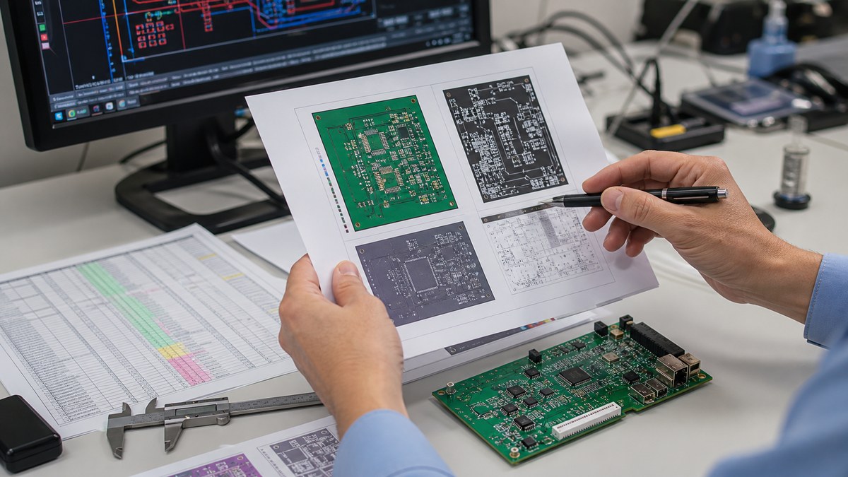
Engineer reviewing PCB files before confirming custom PCB lead time
Incomplete Gerber, BOM, stackup or assembly notes can turn a quick-turn request into a clarification loop.

A common delay is a file set that looks complete but has contradictions. Examples include a board outline that does not match the mechanical drawing, a BOM package that does not match the centroid file, a stackup note that conflicts with impedance requirements, or a surface finish choice that is not suitable for the component package. These issues should be solved before the purchase order is treated as production-ready.

Board Complexity Has More Impact Than Board Size Alone

Lead time usually increases when the board requires more controlled process steps, tighter inspection or less common materials.

Layer count matters, but it is only one part of the schedule. HDI microvias, blind or buried vias, sequential lamination, heavy copper, fine line and space, controlled impedance, unusual thickness, rigid-flex construction and special surface finishes can all add review and production time. If a project needs HDI density, review the board against realistic HDI PCB manufacturing limits before asking for rush delivery.

Material choice also matters. Standard FR4 is usually easier to schedule than a special laminate, ceramic substrate, metal core PCB, RF material or high-temperature stackup. If standard FR4 is acceptable, the FR4 printed circuit board route may reduce sourcing risk. If the design needs special thermal, high-frequency or structural behavior, lead time should include material confirmation.

PCBA Lead Time Depends on Components, Not Only Assembly Speed

For turnkey PCBA, component availability often controls the real delivery date more than placement speed.

A factory may be able to assemble a small batch quickly once all parts are ready, but that does not mean every assembled board can ship quickly. Long-lead ICs, connectors, magnetics, sensors, relays, custom cables, displays and odd passives can delay the start of assembly. If the BOM has obsolete, allocated or region-specific parts, schedule risk should be discussed before the order is placed.

When schedule matters, confirm whether the supplier can support component sourcing, approved alternates, incoming inspection and shortage reporting. A practical BOM review should identify no-stock items, risky single-source parts, package mismatches and parts that require programming or special handling.

When Quick-Turn PCB Manufacturing Is Realistic

Quick-turn service is realistic when the design uses available materials, complete files and a process flow that fits the factory queue.

Fast schedules work best for simple prototypes, standard materials, small or medium panel sizes, common finishes, clean drill data, no unresolved DFM issues and components that are already in stock. A quick-turn request becomes less reliable when the board needs special laminate, multiple lamination cycles, unusual solder mask, tight impedance tolerance, large panels, heavy copper, fixture-based testing or long-lead components.

For assembled prototypes, a dedicated prototype PCB assembly flow can help engineering teams validate a design before locking mass production. If the project must move from prototypes into larger volumes, quick turn PCB assembly should be planned with component supply and test coverage in mind.

Rush Fees Do Not Fix Every Lead Time Problem

Expedited service can compress queue time, but it cannot remove engineering, material or component constraints that still need resolution.

Rush delivery is most useful when the files are clean and the process is standard. It is less useful when the supplier still needs to clarify impedance, stackup, plating, tolerances, test methods, part substitutions or acceptance criteria. Paying for speed before the file package is stable can create rework rather than faster delivery.

A better approach is to ask the supplier which step controls the schedule. If the answer is material sourcing, choose an available material or accept a longer lead time. If the answer is DFM risk, revise the design. If the answer is component shortage, approve alternates or split the build. If the answer is production queue, expedited service may help.

How to Prepare an RFQ for a Reliable Lead Time

A lead-time-ready RFQ should let the supplier quote the board without guessing about design intent, assembly scope or acceptance criteria.

  • Send the final Gerber or ODB++ package, NC drill files and board outline.
  • Include stackup, copper weight, board thickness, material preference and surface finish.
  • Mark impedance, controlled-depth drilling, press-fit holes, castellations or edge plating if used.
  • For PCBA, send BOM, centroid file, assembly drawing, polarity notes and testing requirements.
  • State the target quantity, prototype or production purpose, required delivery date and shipping country.
  • List any parts that cannot be substituted and any parts where alternates are allowed.
  • Ask the supplier to separate fabrication, component sourcing, assembly, testing and shipping time.

Lead Time Risk Checklist Before You Approve Production

Before approval, check the schedule against the real manufacturing risks instead of accepting a single optimistic delivery date.

PCB assembly production line reviewing schedule before shipment
Production lead time should include fabrication, assembly, inspection, packing and logistics, not only machine time.
  • Are all production files approved and version-controlled?
  • Are laminate, copper, solder mask and surface finish available?
  • Do all critical components have stock, alternates or confirmed purchase dates?
  • Does the board need impedance testing, flying probe, fixture test, AOI, X-ray or functional test?
  • Does the first article require engineering approval before the full batch continues?
  • Are packaging, labeling, customs documents and shipping method already defined?
  • Is the promised date based on working days, calendar days or shipment date?

How to Reduce Custom PCB Manufacturing Lead Time Without Raising Risk

The safest way to reduce lead time is to remove uncertainty before production starts.

Use standard materials when possible, keep the first prototype inside common capability, avoid unnecessary special finishes, release a clean BOM, allow qualified alternates and answer DFM questions fast. For PCBA, order critical long-lead components early or let the supplier source parts before the bare boards are finished. For repeat builds, keep the same approved stackup, finish, stencil and test plan unless a change is necessary.

Do not shorten lead time by skipping review on a high-risk board. A missed annular ring issue, wrong footprint, unavailable connector or unclear test requirement can cost more time than a proper review. Good suppliers should be willing to explain the bottleneck instead of only quoting the fastest possible date.

Supplier Questions That Reveal Whether the Schedule Is Reliable

Ask schedule questions that force the supplier to show where the lead time comes from.

  • When does your lead time clock start: quote approval, payment, file approval or material arrival?
  • Which step is the current bottleneck for this board?
  • Are the laminate, solder mask, surface finish chemicals and critical components already available?
  • What changes would shorten the lead time without weakening reliability?
  • Does the quote include electrical test, AOI, X-ray, functional test or only basic inspection?
  • Will the promised date be shipment date or arrival date?
  • What happens if DFM review finds a file issue after order approval?

FAQ About Custom PCB Manufacturing Lead Time

These answers are written for buyers preparing an RFQ, not for one fixed factory schedule.

How long does custom PCB manufacturing take?

It depends on board complexity, material availability and whether assembly is included. Simple prototypes can move much faster than HDI, rigid-flex, ceramic, heavy copper or fully assembled PCBAs. Treat any published number as a starting point and ask for a quote based on your actual files.

When should I start counting PCB lead time?

Count lead time after production files are approved, the order is confirmed and required materials or components are available. Early emails, incomplete Gerbers or unresolved BOM questions should not be treated as production time.

What files are needed to confirm custom PCB lead time?

For bare boards, send Gerber or ODB++ files, drill files, board outline, stackup, material, thickness, copper weight and finish. For PCBA, add BOM, centroid file, assembly drawing, polarity notes and test requirements.

Does PCBA always add more lead time than bare PCB fabrication?

Usually yes, because assembly needs stencil preparation, component sourcing, placement, soldering, inspection and sometimes testing. The largest delay is often component availability, not the placement process itself.

Can I reduce lead time by using standard FR4?

Often yes. Standard FR4, common board thickness, common copper weight and common surface finish are easier to schedule than special laminate, ceramic, RF material, metal core, rigid-flex or unusual process requirements.

What makes HDI or rigid-flex boards slower?

HDI and rigid-flex designs may need sequential lamination, laser drilling, tighter registration, controlled impedance, special materials and extra inspection. These steps are useful, but they should be planned instead of treated like standard quick-turn FR4 work.

Do rush fees guarantee delivery?

No. Rush fees may reduce queue time, but they cannot remove material shortages, unresolved DFM issues, unavailable components or unclear test requirements. Ask which step controls the schedule before approving an expedite charge.

How can I avoid delays after placing the order?

Freeze the file revision, respond to DFM questions quickly, approve part alternates early, confirm test requirements and avoid changing quantity, finish or shipping method after production starts.

Should I split prototypes and production into separate orders?

For new designs, yes in many cases. A prototype order can validate the layout, BOM, assembly process and test plan before a larger production batch. This reduces the risk of repeating an error at volume.

What should a supplier include in a clear lead time quote?

The quote should separate engineering review, material or component sourcing, bare PCB fabrication, assembly, inspection, packing and shipping. It should also state whether the date means completion, shipment or delivery.

Final Buying Advice

Custom PCB manufacturing lead time is predictable when the supplier sees the full design, confirms materials and separates each production stage. Before approving a rush order, ask what is slowing the schedule and whether a file, material or BOM change would reduce risk. If you are planning PCB fabrication, turnkey PCBA, prototypes or mass production, send your Gerber, BOM and assembly files to the Best Technology engineering team at sales@bestpcbs.com for a lead time and quotation review.

You may also like

Custom PCB, Printed Circuit Board Maker, Tech-Driven
Tuesday, June 3rd, 2025

Printed circuit board maker is the first thing many electronics developers search for when starting a new design. Whether you are prototyping or scaling to full production, choosing the right partner can save you time and cost. This blog explores global PCB manufacturing options and why EBest Circuit (Best Technology) stands out in this crowded field.

EBest Circuit (Best Technology) is a tech-driven printed circuit board maker, providing a wide range of PCBs, like FR4, ceramic PCB, MCPCB, and PCB assembly. We can offer custom PCB and custom solutions to suit your project needs. You can rest assured that Printed Circuit Board quality making by EBest Circuit (Best Technology) is guaranteed.  Kindly contact us at sales@bestpcbs.com for any custom PCB needs.

Custom PCB, Printed Circuit Board Maker, Tech-Driven

Printed Circuit Board Maker in India

India has become a growing hub for PCB manufacturing, thanks to its competitive pricing, increasing technological advancement, and government support. Many global brands now turn to Indian PCB makers for high-volume and prototype solutions.

  1. AT&S India Pvt. Ltd. (Andhra Pradesh)
    • A subsidiary of Austria’s AT&S Group, this company operates one of India’s most advanced PCB factories. It focuses on high-end PCBs for automotive, medical, and industrial applications. With state-of-the-art facilities and automation, AT&S meets global quality standards like IATF16949 and ISO13485.
  2. Shogini Technoarts Pvt. Ltd. (Pune)
    • With over three decades in the industry, Shogini is known for producing single-sided, double-sided, and multilayer PCBs. Their capabilities support small to medium-volume production runs and a variety of industries including lighting, consumer electronics, and automotive.
  3. Genus Electrotech Ltd. (Gujarat)
    • Genus is a vertically integrated manufacturer offering everything from PCB design to final assembly. They serve a wide range of sectors including power, smart meters, and consumer products. Their manufacturing meets global standards and is RoHS-compliant.

India’s PCB makers are fast adapting to global demand with investments in automation and quality control. For companies looking for affordability with improving capabilities, India presents a strong option.

Custom PCB

Printed Circuit Board Maker in Canada

Canada’s PCB industry is shaped by high standards, clean manufacturing processes, and strong R&D. Canadian PCB makers are known for their quality assurance and capability to handle complex, multilayer boards.

  1. Bittele Electronics (Toronto, Ontario)
    • Bittele offers turnkey PCB assembly and manufacturing services, specializing in low-volume and prototype runs. They are known for their quick turnaround, and strong online ordering system. They serve clients globally, especially in North America.
  2. Candor Industries Inc. (Toronto, Ontario)
    • Candor stands out with its environmentally friendly processes and capability to handle high-frequency and HDI PCBs. They have an open-culture model with direct communication between engineers and customers, which supports complex design solutions.
  3. Circuits Central Inc. (Ontario)
    • Circuits Central provides full-service PCB fabrication and assembly. With a focus on industrial, medical, and telecom sectors, they offer design support, rapid prototyping, and full manufacturing runs. Their facility meets ISO standards and supports high-complexity builds.

Canadian PCB makers provide a mix of precision, environmental responsibility, and technical expertise. If your project needs detailed design support and compliance with international standards, Canada is a strong choice.

Printed Circuit Board Maker UK

The UK’s PCB sector is known for engineering excellence, with a strong emphasis on R&D and high-end industrial applications. Manufacturers here focus on performance, reliability, and customization.

  1. Newbury Electronics Ltd. (Berkshire)
    • This company offers rapid PCB prototyping and manufacturing services. They support everything from single-sided boards to complex multilayer PCBs. With in-house assembly and CAD support, Newbury is a top choice for engineers looking for fast development cycles.
  2. Trackwise Designs Plc (Gloucestershire)
    • Trackwise specializes in advanced RF and flexible PCBs, especially for aerospace and automotive sectors. Their patented length-unlimited FPC technology is well-known across Europe. They serve as a strategic partner for high-frequency and high-reliability needs.
  3. Exception PCB Ltd. (Wiltshire)
    • Exception PCB serves critical industries such as defense, aerospace, and medical devices. They provide multilayer and high-speed PCBs with advanced quality assurance and traceability systems. Their global customer base values their engineering strength and production precision.

UK PCB manufacturers offer engineering-driven services with tight tolerances and customization. For projects that require reliability and innovation, British PCB makers remain among the top-tier options globally

Printed Circuit Board Maker

How Long Does It Take to Make a Printed Circuit Board?

Timeframes vary. For simple single-layer PCBs, it may take 24-48 hours. Complex multilayer boards may need 7-10 days. Delays often come from unclear Gerber files, missing BOMs, or design flaws. That’s why working with a responsive printed circuit board maker helps reduce back-and-forth and speeds things up.

How Many Layers Can a Printed Circuit Board Have?

A printed circuit board can have 1 to over 40 layers, depending on design needs. Consumer electronics often use 2 to 8 layers. Aerospace or telecom PCBs go higher. EBest Circuit (Best Technology) supports a wide layer range with excellent impedance control and layer stack-up guidance.

How to Make a Printed Circuit Board?

It starts with design. Once your schematic and layout are complete, generate Gerber files. Share them with your PCB partner. The process involves lamination, drilling, plating, etching, and solder mask application. A reliable printed circuit board maker will guide you at each step, especially during DFM (Design for Manufacturability).

Tech-Driven

Why Should You Choose EBest Circuit (Best Technology) as Your Trusted Printed Circuit Board Maker?

EBest Circuit (Best Technology) solves key pain points every customer faces. Let’s break it down:

1. Reliable Quality and On-Time Delivery

Many customers struggle with delayed delivery or inconsistent quality. We operate under ISO9001, ISO13485, IATF16949, and AS9100D systems. From material incoming checks to final inspection, every step meets international standards. Automated inspection reduces errors and improves reliability.

2. Full Compliance and Certification

We’re fully RoHS, WEEE, and IPC compliant. Plus, our ESD protection covers every handling step. With a strong audit-ready system, we meet the strictest vendor verification protocols. That builds long-term trust and collaboration with top brands worldwide.

3. Advanced Design and Engineering Support

Some customers worry about lacking internal engineers. Our team helps with design review, BOM optimization, and stack-up suggestions. Early engagement avoids late-stage redesigns. Our DFM tools simplify development and lower your risk.

4. Fast Lead Times

Multilayer boards and HDI PCBs often have long cycles. We respond with lean production and MES-driven planning. Our digital system tracks each order step-by-step. Need a prototype in 2 days? We’ve got you.

5. Strong Quality Control System

PCB defects like poor soldering, scratches, or delamination are common pain points. Our AI-driven visual inspections detect micro-defects that even trained eyes miss. Multiple QC stages—AOI, X-ray, ICT, and FQC—guarantee top quality with minimal waste.
6. Fast Response and Human Support

We understand the importance of clear communication. Especially in R&D phases or small-batch trials, a slow response ruins progress. Our engineering support runs 24/7, and sales teams speak fluent English. Quick replies, accurate quotes, and expert suggestions come standard.

7. Tech-Forward Manufacturing

We invest in smart systems. AI inspection, automated production, and MES dashboards enable real-time monitoring. From plating thickness to hole alignment, precision is built into our lines. That reduces rework and boosts throughput. Our smart factory plan hits 50% coverage by 2025.

8. Sustainable Manufacturing

As environmental standards rise, so do our green efforts. Our lines use water recycling, low-VOC materials, and waste tracking. We’re pushing to grow our share in the green PCB market, which is forecast to hit 45% in 2025. Customers love this proactive approach.

Printed Circuit Board Maker, Tech-Driven

In a nutshell, being a printed circuit board maker today isn’t just about producing boards. It’s about speed, trust, service, and innovation. EBest Circuit (Best Technology) understands your demands and brings real solutions. We deliver high-quality boards fast, support your design, and adapt to complex requests. From HDI to rigid-flex, from prototypes to mass production—our team is ready to help you build better. Let us help you move faster, reduce errors, and grow smarter. Get in touch with us at sales@bestpcbs.com for your next PCB quote. With EBest Circuit (Best Technology), every board counts.

You may also like