PCB manufacturing PCB manufacturing
Home > Blog

pcb manufacturing

Custom PCB Design for Industrial Use: Enclosure, Power and I/O Checks
Monday, July 13th, 2026
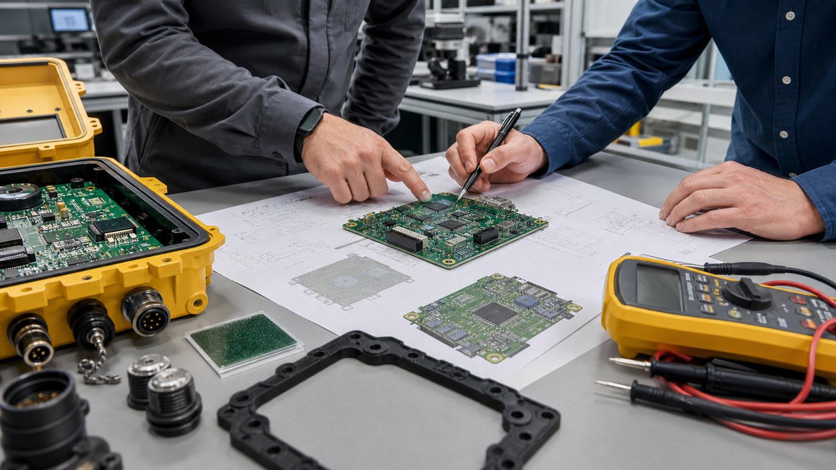
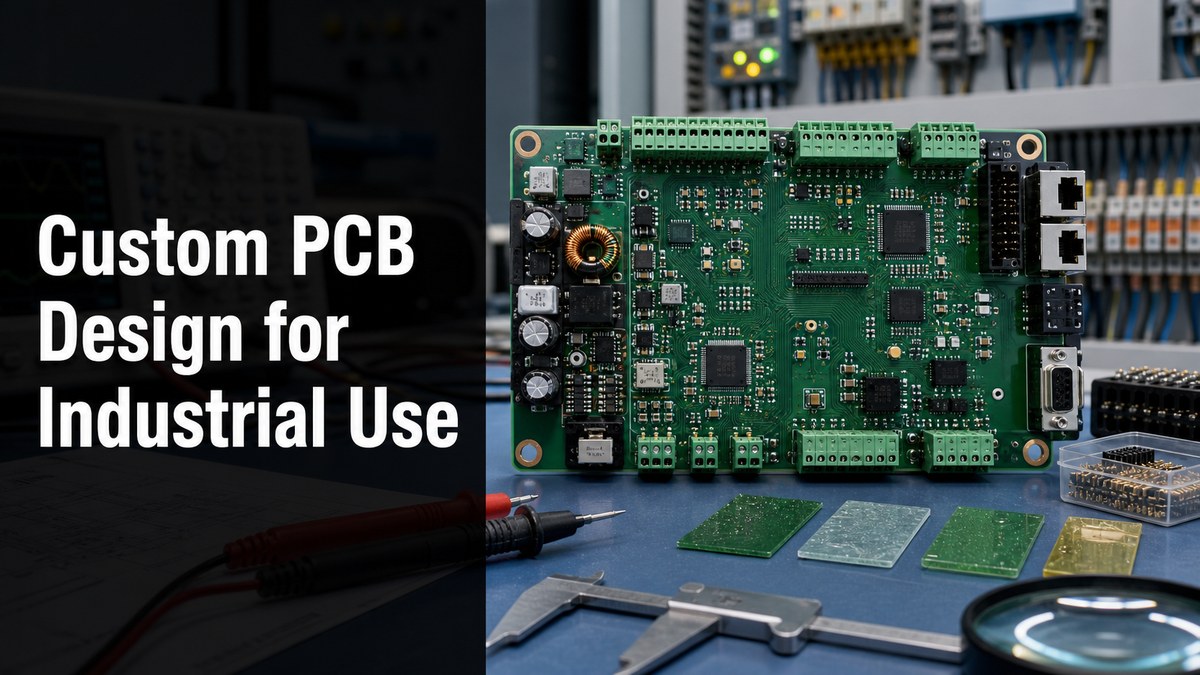
Custom PCB design for industrial use with terminal blocks, power circuitry and test tools

Custom PCB design for industrial use means designing the bare board and assembly around the real installation: enclosure size, field wiring, power noise, vibration, temperature, moisture, service access and test coverage. A board that works on a lab bench can still fail in a cabinet, pump controller, sensor node or factory gateway if the PCB layout ignores connectors, grounding, protection, mounting and production test points.

For an industrial product, the best PCB design brief is not only a schematic and a Gerber file. It should explain the operating voltage range, load current, connector map, enclosure limits, ambient temperature, coating or potting needs, expected service life, and how the board will be tested before shipment. Those details help the PCB manufacturer catch risk before the design moves into fabrication and assembly.

What Is Custom PCB Design for Industrial Use?

Custom PCB design for industrial use is the process of turning an industrial product requirement into a manufacturable board layout that can survive field wiring, power variation, mechanical stress and repeatable production testing. It is different from a generic electronics board because the installation environment becomes part of the design input.

An industrial controller, power monitor or equipment interface often needs larger terminal blocks, screw mounting holes, isolation gaps, surge protection, clear service labels and room for hand tools. The base material may still be a standard FR4 Printed Circuit Board, but the layout rules, copper weight, coating decision and connector placement should be chosen for the real equipment, not for a clean prototype demo.

Start With the Enclosure, Not Only the Circuit

The enclosure fixes many PCB design decisions before trace routing begins. Board outline, mounting holes, connector direction, LED visibility, cable bend radius, airflow and service clearance all depend on the box or cabinet where the board will be installed.

Before layout, confirm the board outline against the mechanical drawing. Check whether connectors must face a panel opening, whether screw terminals need finger access, and whether high-voltage or high-current areas need physical separation from signal wiring. If the board is part of a complete product rather than a loose PCB, coordinate early with the Box Build Assembly plan so cable routing, labels, displays and mechanical fasteners are not solved after the PCB is already finished.

Enclosure factor PCB design check Why it matters
Mounting points Hole size, copper keep-out, washer clearance Prevents cracked solder joints and board flex
Panel connectors Connector height, orientation and access Avoids cable strain and rework during assembly
Airflow Heat source placement and component height Reduces hot spots in sealed or crowded cabinets
Coating or potting Keep-out around connectors, switches and test pads Prevents coating from blocking service points
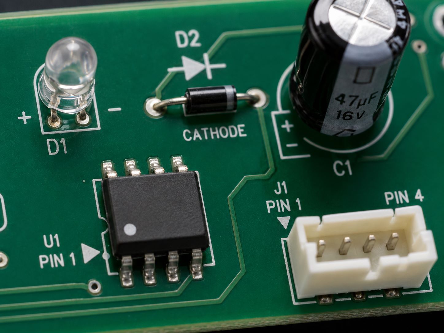
Service access Readable silkscreen and reachable fuses/test points Helps technicians diagnose the unit in the field

Design the Power Input for Real Factory Conditions

Industrial PCB power design should assume voltage variation, switching noise, inrush current and wiring mistakes instead of assuming a perfect bench supply. The exact protection scheme depends on the product, but the layout should reserve room for protection, filtering and thermal relief.

For DC industrial boards, check reverse-polarity protection, fuse or resettable protection, surge or transient suppression, input filtering, regulator heat, copper width and connector current rating. For boards that switch motors, relays, heaters or solenoids, keep noisy current loops compact and separated from sensors, analog inputs and communication traces. High-current or high-heat industrial applications may need heavier copper, metal-core materials, ceramic substrates or another special PCB structure instead of a basic two-layer FR4 board.

Protect I/O Before It Reaches the MCU

Field I/O is one of the most common weak points in industrial PCB design because long cables carry noise, ESD, surge and wiring errors directly to the board edge. Treat every external connector as a risk entry point.

Place ESD or surge protection close to the connector when required. Keep isolation slots, creepage and clearance appropriate for the voltage category. Put pull-ups, filtering, common-mode chokes or termination near the interface they protect. For RS-485, CAN, Ethernet, sensor inputs or dry-contact I/O, make grounding and shield termination choices early so the PCB layout does not fight the installation wiring later.

Connector selection also affects assembly and sourcing. A design that depends on a rare terminal block or long-lead-time relay may be difficult to build during a shortage. Early Component Sourcing review helps confirm package availability, approved alternates and whether the BOM can support prototype and production builds.

Plan DFM, Assembly and Test Points Together

A good industrial PCB layout is not finished until assembly access and test coverage are planned. If test pads, programming headers and fixture access are added at the end, the board may pass a prototype build but become slow or expensive in production.

Confirm component orientation, panelization, fiducials, solder mask clearance, through-hole access, connector height and coating keep-outs before release. For the assembled product, define which rails, interfaces and functional outputs must be checked. The layout should include accessible test pads for ground, input voltage, main regulators, communication signals and critical sensor lines. A related engineering guide on Circuit Board Test Points can help teams decide which signals deserve fixture access before the first production batch.

If the supplier will handle both PCB fabrication and PCBA, PCB Assembly, SMT, PCB SMT by EBest Circuit (Best Technology), send the assembly drawing, BOM, pick-and-place file, test plan and coating requirements together. Separating fabrication questions from assembly questions often hides problems until parts are already on order.

Industrial PCB Design Checklist Before RFQ

The RFQ package should let the manufacturer review risk, not just quote a board size and layer count. Missing details usually turn into delayed questions, wrong assumptions or rework.

  • Gerber files, drill files, stackup notes and controlled impedance needs if applicable.
  • Board outline with enclosure drawing or DXF when connectors and mounting holes are critical.
  • BOM with manufacturer part numbers, approved alternates and lifecycle notes.
  • Assembly drawing with polarity marks, connector orientation and no-fit parts.
  • Expected environment: temperature, humidity, vibration, dust, splash, coating or potting.
  • Power input range, load current, surge concerns and isolation requirements.
  • Test requirements: programming, in-circuit checks, functional test and inspection points.
  • Packaging and box-build notes if the PCB ships as a complete module.

Common Mistakes That Make Industrial Boards Hard to Build

Most industrial PCB mistakes are not exotic layout errors; they are practical mismatches between the board, the cabinet, the wiring and the production process. Catching them before fabrication saves more time than debugging them after assembly.

Mistake Likely result Better design action
Connectors placed without cable clearance Field wiring bends sharply or blocks the cover Check cable path against enclosure CAD
No test access for power rails Production test becomes slow and manual Add test pads near regulators and protected I/O
Small copper paths for load current Heating, voltage drop or early failure Check copper width, copper weight and thermal relief
Protection parts far from connectors ESD or surge reaches sensitive ICs first Place protection near external entry points
No alternates for industrial connectors Build delay during component shortage Review BOM availability before final layout

Supplier Questions for an Industrial PCB Project

Use supplier questions to check whether the PCB manufacturer understands the product conditions, not only the drawing package. The answers should expose DFM gaps early.

  • Can you review connector clearance against the enclosure drawing?
  • Do any parts in the BOM have long lead time, EOL risk or weak alternates?
  • Which test points are needed for production fixture testing?
  • Should the board use thicker copper, different laminate, coating or selective keep-outs?
  • Can fabrication, assembly, coating and box build be reviewed as one workflow?
  • Which inspection records or test reports will be provided with the finished boards?

FAQ

What files are needed for a custom PCB design for industrial use?

Send Gerber and drill files, BOM, pick-and-place file, assembly drawing, board outline, enclosure drawing if available, test requirements and operating environment notes. For industrial boards, the enclosure, connector map, power range and coating requirements are often as important as the PCB data itself.

Does every industrial PCB need conformal coating?

No. Coating depends on moisture, dust, chemical exposure, voltage spacing and service requirements. If coating is needed, the PCB should include keep-outs around connectors, switches, jumpers, labels and test pads so coating does not block assembly or maintenance.

How should I choose materials for an industrial PCB?

Start with temperature, current, voltage, mechanical load and heat dissipation. FR4 is common for many control boards, but high-current, high-temperature, RF, heavy copper, metal-core or ceramic requirements may call for a different stackup or special PCB process.

Why do industrial PCBs need more test points than simple prototypes?

Production builds need repeatable checks. Test points give fixtures access to voltage rails, programming pins, communication lines and critical I/O. Without them, technicians may rely on slow manual probing or miss faults that only appear after installation.

Final Recommendation

For custom PCB design for industrial use, review the board as part of a field product: enclosure, wiring, power, I/O protection, assembly, sourcing and test coverage. The strongest RFQ package gives the manufacturer enough context to find DFM, BOM and reliability risks before the first boards are built.

You may also like

Custom PCB Design for Agriculture: Sensors, Power and Field Reliability
Monday, July 13th, 2026
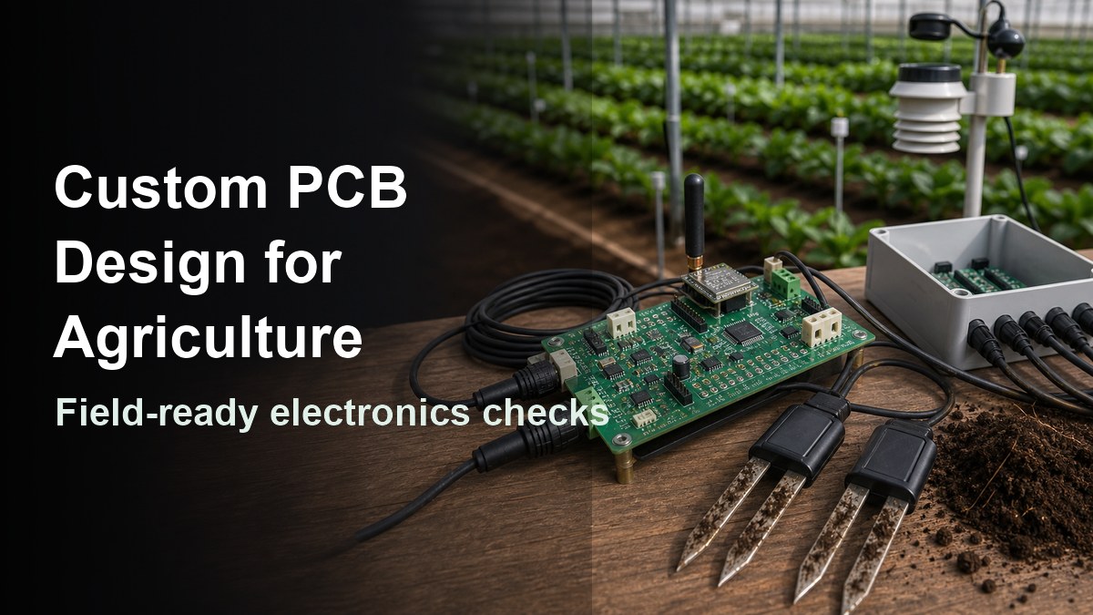
Custom PCB design for agriculture with field sensor electronics and greenhouse equipment
Custom agriculture PCB projects need field-ready design choices before fabrication and assembly.

Custom PCB design for agriculture means designing a circuit board that can survive moisture, dust, vibration, unstable power, long cable runs, sensor drift and outdoor service conditions. A board used inside a soil sensor, irrigation controller, greenhouse monitor, livestock tracker or farm machine is not just a normal indoor PCB with a different enclosure.

The safest approach is to design the PCB, enclosure, connectors, power input, sensor interfaces, wireless layout and test plan together. If these decisions are left until production, the project may pass a bench test but fail after rain, washing, temperature cycling, fertilizer exposure or field vibration.

What Does Custom PCB Design for Agriculture Need to Solve?

Agriculture PCB design must solve environmental exposure and measurement reliability at the same time. The board may need to read weak sensor signals, run from battery or solar power, communicate wirelessly, drive pumps or valves, and keep working in wet, dusty and electrically noisy locations.

For a farm device, the PCB is often part of a larger field system. The same board may connect to soil probes, temperature sensors, humidity sensors, GPS modules, LoRa, NB-IoT, Bluetooth, motor drivers, solenoids or user controls. That mix creates real trade-offs: sensor accuracy needs clean analog layout, wireless modules need controlled antenna space, and outdoor wiring needs surge and reverse-polarity protection.

This is why the design review should start from the use case, not only from the schematic. A greenhouse data logger, a drip irrigation controller and a tractor-mounted control module can all be called agriculture electronics, but their PCB risks are different.

Application Main PCB design concern What to confirm before RFQ
Soil and moisture sensor node Low-noise sensing, waterproof cable entry, battery life Sensor type, probe connector, coating or potting limits
Irrigation controller Valve current, relay or MOSFET heat, surge protection Load current, cable length, transient protection and enclosure plan
Greenhouse monitor Humidity, condensation, wireless stability Operating temperature, antenna position and conformal coating area
Farm machine electronics Vibration, wide input voltage, connector strain Mounting method, power input range, harness and test standard
Livestock or asset tracker Battery life, RF performance, mechanical size Battery chemistry, sleep current target, antenna keep-out area

Which Field Conditions Change Agriculture PCB Design?

Moisture, dust, chemicals, temperature swing, vibration and unstable power are the conditions that most often change agriculture PCB design. If the board is specified like an office device, the first field failure may come from corrosion, connector leakage or a power transient rather than from the core circuit.

Humidity and condensation are common in greenhouses, irrigation cabinets and outdoor sensor boxes. If moisture can reach the PCB surface, high-impedance sensor circuits may drift and exposed copper may corrode. Designers should decide early whether the board needs conformal coating, selective coating keep-out zones, potting, sealed connectors or a vented enclosure.

Dust, mud and fertilizer residue can create another problem: they trap moisture and make cleaning difficult. Connector position, enclosure drain paths and service access matter. A connector that works in a lab may become a failure point if it faces upward, sits near a water path or lacks strain relief.

Power input also needs attention. Agricultural equipment may use long cable runs, solar charging, batteries, vehicle power or shared power rails. The PCB may need reverse-polarity protection, input filtering, surge suppression, brownout behavior and enough copper width for valve or motor loads. For material selection and base board planning, the FR4 printed circuit board page is a useful internal reference for common FR4 PCB options.

How Should Sensors, RF and Power Be Planned?

Sensors, RF and power should be planned as three interacting systems, not separate blocks. A low-power wireless agriculture board may fail if the antenna is blocked by the enclosure, if the sensor trace runs beside a switching node, or if the battery rail collapses during transmission.

Start with the sensor interface. Soil probes, pH probes, temperature sensors, flow meters and pressure sensors may use analog voltage, resistance, frequency, I2C, SPI, UART, RS-485 or other interfaces. Weak analog signals need short routing, guard spacing where needed, stable references and a quiet ground strategy. Digital sensors need connector mapping, ESD protection and firmware-accessible diagnostics.

Wireless planning should be handled before the mechanical layout is frozen. LoRa, Wi-Fi, Bluetooth, NB-IoT and cellular modules each need antenna clearance, ground reference, keep-out areas and sometimes matching components. If the enclosure is metal, wet or mounted near machinery, RF performance may change. The article on IoT sensor PCB assembly is a related page for sensor modules, wireless devices and PCBA test planning.

Power design should match how the device will really be used. A solar-powered field node may care most about sleep current and battery charging safety. An irrigation controller may care about surge protection and load current. A machine-mounted PCB may need wider input voltage tolerance, filtering and vibration-resistant connectors. Put current paths, heat sources and sensitive sensor traces in different layout zones when possible.

What Materials and Protection Choices Matter?

Material and protection choices matter because agriculture electronics often fail at the boundary between PCB, enclosure and environment. FR4 may be suitable for many projects, but the design still needs the right copper weight, solder mask coverage, surface finish, coating decision and mechanical support.

For many sensor boards and controllers, standard FR4 is a practical starting point. High Tg FR4, heavier copper, rigid-flex construction, aluminum PCB or ceramic PCB may be considered when temperature, current, bending, heat spreading or size constraints justify them. Do not choose a special material only because the application sounds harsh; choose it because the electrical, thermal or mechanical requirement makes it necessary.

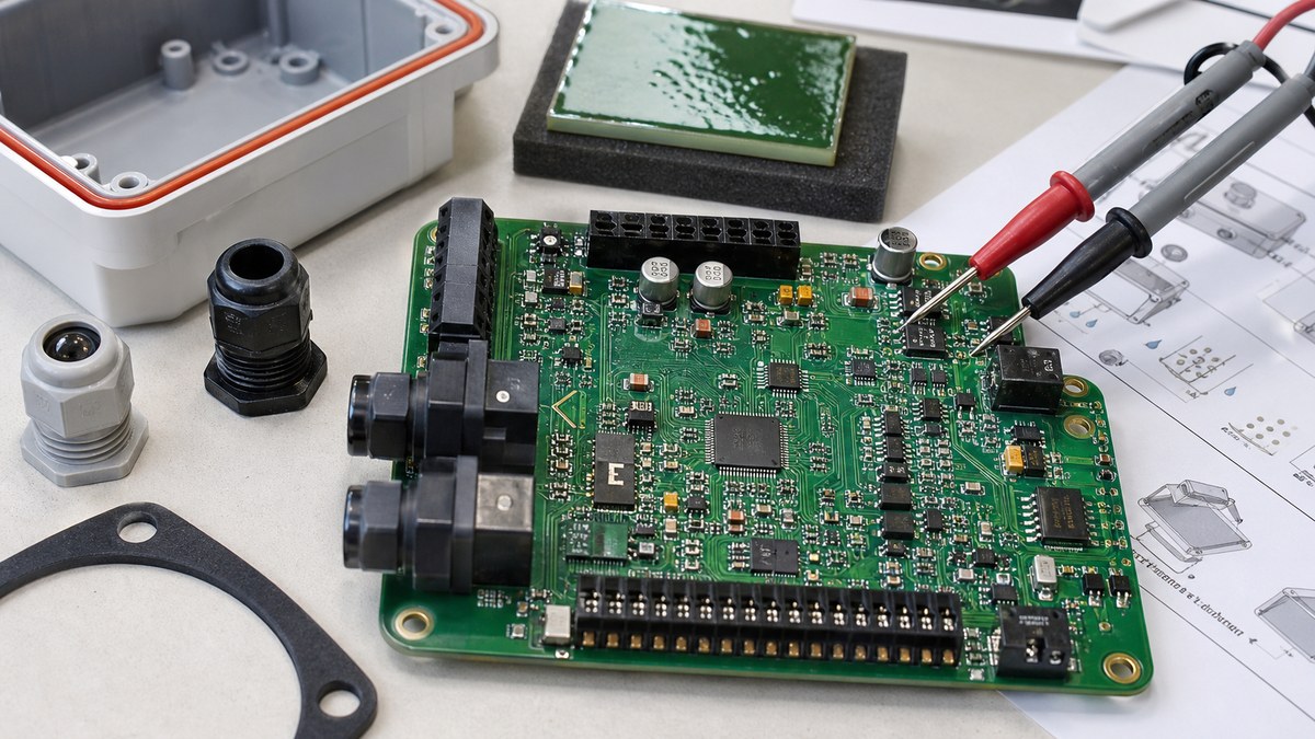
Protection should be discussed with the manufacturer before assembly. Conformal coating can protect against moisture and residue, but it may interfere with connectors, test pads, switches, LEDs, sensor membranes or calibration points. Potting can improve sealing and vibration resistance, but it can make rework impossible and trap heat. A gasketed enclosure helps, but the PCB still needs proper connector orientation and creepage/clearance decisions.

Agriculture sensor PCB protection review with enclosure gasket, cable glands, coating sample and probes
Coating, enclosure sealing and connector choices should be reviewed before PCB fabrication and assembly.

If the device will face rain, spray, condensation or washing, compare the enclosure plan with PCB-level protection. The waterproof PCB guide explains coating, potting and protection trade-offs that are especially relevant to farm electronics.

How Should Connectors, Enclosures and Assembly Be Specified?

Connectors, enclosures and assembly should be specified before the PCB layout is released. In agriculture devices, many failures start at cable entry points, unsupported connectors, difficult assembly steps or missing test access.

Use locking or sealed connectors where field wiring is exposed to vibration, splash or repeated service. Place connectors so cables can be strain relieved and routed without sharp bends. If the device needs field replacement, the connector choice should match what a technician can handle with gloves, dust and limited visibility.

The enclosure affects PCB shape, mounting holes, connector height, antenna position, cable glands and service access. If the board needs a conformal coating process, mark coating keep-out areas in the drawing. If it needs potting, confirm component height, heat dissipation and whether any part must remain exposed to air.

Assembly files should not be treated as an afterthought. A clean BOM, centroid file, polarity notes, programming instructions, coating notes and test requirements reduce mistakes. For PCBA planning, the PCB assembly and SMT service page is the relevant service page to link when the article discusses prototype or production assembly.

What Testing Should Be Done Before Field Use?

Testing should prove that the PCB works electrically and that the field risks have been addressed. For agriculture electronics, a simple power-on test is not enough if the product will face moisture, vibration, long cables, battery sag or wireless range limits.

Start with normal manufacturing tests: visual inspection, AOI where applicable, continuity checks, programming, functional test and current consumption measurement. Add application-specific tests such as sensor calibration, wireless transmission, load switching, sleep current, input overvoltage behavior, reverse-polarity response and connector continuity after cable movement.

Environmental and mechanical validation depends on the project risk. A prototype may need humidity exposure, temperature cycling, splash simulation, vibration checks or enclosure sealing review. These tests should be defined with realistic limits rather than vague wording such as “outdoor grade.” If no formal standard is specified, record the actual test condition in the engineering notes.

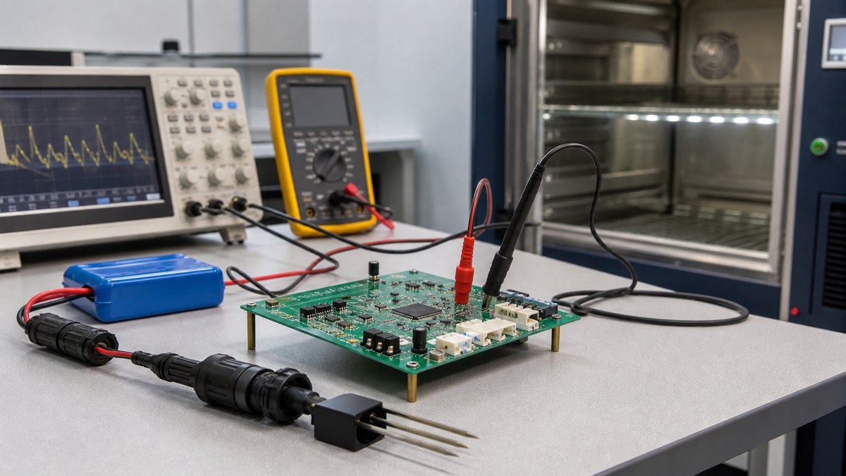
Agriculture PCB field reliability testing with probes, battery input, connector harness and environmental chamber
Field reliability checks should include power input, connectors, sensor behavior and environmental exposure.

When writing the RFQ, include the required inspection method instead of assuming the supplier will infer it. The PCB test equipment page can support sections about inspection capability, while the custom PCB board fabrication guide is useful for file, stackup and process-check details before quotation.

Agriculture PCB Design Checklist for RFQ Files

A good RFQ package should let the PCB manufacturer understand the electrical design, field environment, assembly process and validation requirements. Missing environmental or test details often lead to a cheaper quote that does not match the real project risk.

  • Gerber or ODB++ files, drill files, board outline and stackup notes.
  • Schematic or design notes for sensor inputs, power input and communication interfaces.
  • BOM, centroid file, polarity notes and approved substitutes if assembly is required.
  • Material preference, copper weight, surface finish and solder mask requirements.
  • Enclosure drawing, mounting hole position, connector height and cable exit direction.
  • Coating, potting or no-clean requirements, including keep-out zones.
  • Operating temperature range, humidity exposure, splash/dust exposure and vibration concern.
  • Programming, calibration, current consumption and functional test requirements.
  • Prototype quantity, pilot quantity, mass production estimate and expected revision plan.
  • Any standards, customer test methods or acceptance criteria that must be followed.

If the agriculture device uses long cables, wireless modules, battery power or outdoor enclosures, send mechanical and use-case information early. The PCB supplier can review DFM, panelization, assembly handling and test access only if those details are visible before fabrication.

FAQ About Custom PCB Design for Agriculture

What is custom PCB design for agriculture?

Custom PCB design for agriculture is the process of designing a circuit board for farm, greenhouse, irrigation, livestock, sensor or machinery electronics. It must consider the circuit function and the field environment together, including moisture, dust, vibration, power input, connectors, sensor accuracy and testing.

Can a normal PCB be used in agricultural electronics?

A normal FR4 PCB can be used in many agriculture devices, but only if the design also handles enclosure sealing, connector protection, coating or potting needs, power input risk and test access. The problem is usually not the word “FR4”; it is whether the board was designed for field exposure.

What sensors are common in agriculture PCB projects?

Common sensors include soil moisture, temperature, humidity, light, pH, pressure, flow, GPS, accelerometers and gas sensors. The PCB layout should match the sensor interface. Analog sensors need noise control, while digital and wireless sensor modules need connector, ESD and firmware test planning.

Does an agriculture PCB need conformal coating?

It depends on the exposure level. Coating is useful for humidity, condensation and light contamination, but it should not cover connectors, switches, some sensors, programming pads or calibration areas. Decide coating zones before assembly, not after the finished PCB already has access problems.

What power problems affect agriculture electronics?

Battery sag, solar charging variation, long cable voltage drop, reverse polarity, pump or valve transients and vehicle power spikes can all affect agriculture PCBs. The design may need input filtering, TVS protection, fusing, reverse-polarity protection, brownout handling and enough copper width for load current.

How should wireless modules be placed on farm device PCBs?

Wireless modules should be placed with the antenna keep-out area, enclosure material, ground reference and cable locations in mind. A module that works on a bench may lose range inside a metal box, near wet soil, beside a battery pack or under a poorly positioned cable harness.

What files should I send for an agriculture PCB quote?

Send Gerber or ODB++ files, drill data, board outline, stackup, BOM, centroid file, enclosure drawing, connector information, coating or potting notes, environmental conditions, test requirements and expected quantities. If the project includes firmware loading or calibration, include those instructions too.

Is potting better than conformal coating for farm electronics?

Potting can provide stronger sealing and vibration support, but it can trap heat and prevent rework. Conformal coating is lighter and easier to inspect, but it does not seal the whole product. The right choice depends on moisture exposure, service needs, heat and mechanical stress.

How can buyers reduce prototype risk?

Build the first prototype with test points, connector access, programming access and clear environmental notes. Test power input, sensor reading, wireless range, current consumption and enclosure sealing before mass production. Do not wait for a large batch to discover that a connector, antenna or coating zone is wrong.

Should agriculture PCB design be handled before or after enclosure design?

It should be handled together with enclosure design. Board outline, antenna location, connector direction, gasket pressure, cable strain relief, coating keep-outs and service access all depend on the enclosure. Treating the enclosure as a late packaging step often creates avoidable redesign.

Final Supplier Notes for Agriculture PCB Projects

Agriculture electronics are usually judged in the field, not only at the lab bench. A good custom PCB design for agriculture should make the sensor readings stable, the wireless link practical, the power input protected, the connectors serviceable and the production test clear.

Before ordering, review the field environment, enclosure, cable harness, coating plan, power input and test requirements with the PCB supplier. If you are sourcing custom PCB design, PCB fabrication or PCB assembly for agriculture sensors, irrigation controllers, greenhouse devices or farm equipment, send your files and field requirements to our engineering team for DFM review and quotation at {contact_email}.

You may also like

Custom PCB Board Fabrication
Sunday, July 12th, 2026
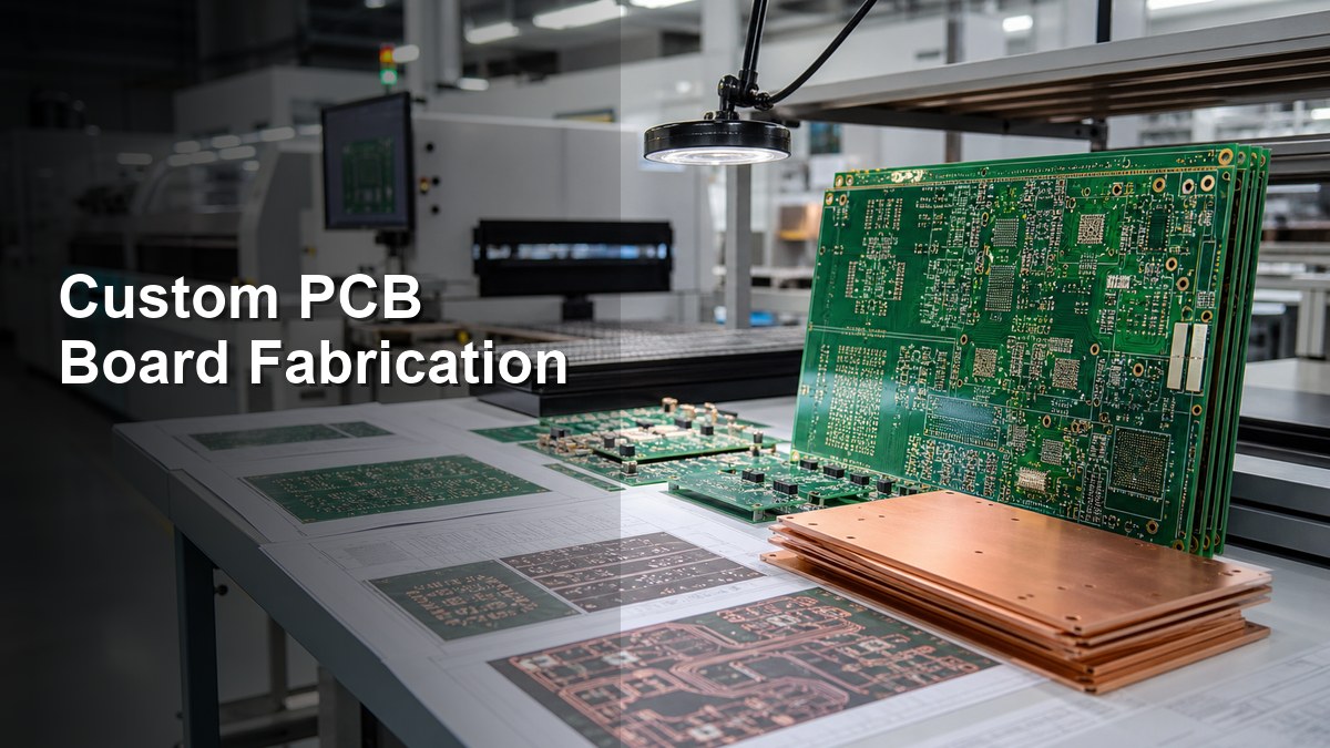
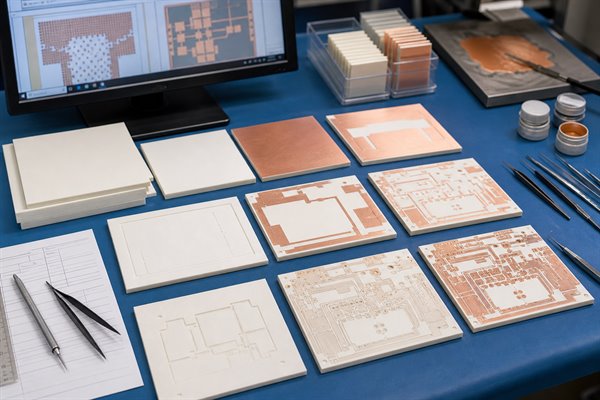
Custom PCB board fabrication with circuit boards, copper panels and manufacturing documents
Custom PCB board fabrication works best when the supplier can review the design intent, materials, stackup and inspection needs before production starts.

Custom PCB board fabrication is the process of turning production-ready design data into a physical printed circuit board built to a specific stackup, material, copper weight, surface finish, tolerance and inspection requirement. A reliable fabrication order is not defined only by board size or layer count. It depends on clean Gerber or ODB++ data, drill files, material availability, manufacturable design rules, controlled process steps and clear acceptance criteria.

For engineers and buyers, the most useful question is not simply “who can make a custom PCB?” The better question is “what information does the fabricator need to build this board correctly the first time?” This guide explains the file package, material decisions, fabrication steps, inspection checks and supplier questions that matter before RFQ.

What Is Custom PCB Board Fabrication?

Custom PCB board fabrication means manufacturing a bare PCB from a customer-specific design rather than buying a standard off-the-shelf board.

The design may be a simple two-layer FR4 board, a dense multilayer board, an HDI board, a heavy copper power board, a metal-core board, a ceramic substrate, or another application-specific construction. The fabricator prepares production tooling from the supplied data, images the copper layers, drills holes, plates vias, applies solder mask and legend, adds the chosen surface finish, routes or scores the outline, and tests the board before shipment.

A custom board gives the designer control over shape, connector position, layer structure, impedance, copper width, heat path, mounting holes and assembly fit. That control also creates responsibility: unclear design notes, missing drill files or unrealistic tolerances can delay production or create boards that are technically built but not suitable for the final product.

Files Needed Before a PCB Can Be Fabricated

A fabricator can only confirm price, lead time and manufacturability when the production file package describes the board without guessing.

For bare PCB fabrication, send Gerber or ODB++ files, NC drill files, board outline, layer stackup, copper weight, finished thickness, material requirement, solder mask color, legend color, surface finish, impedance notes, controlled-depth drilling notes, special plating requirements and a fabrication drawing if tolerances matter. If the board will later be assembled, include the BOM, centroid file and assembly drawing early so the bare board can support the assembly process.

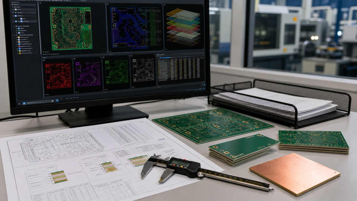
PCB fabrication file review with CAM layers, drill drawing, sample boards and calipers
File review should catch stackup, drill, outline, material and tolerance issues before the board enters production.

Common file problems include an outline that does not match the mechanical drawing, plated and non-plated holes mixed in one unclear drill file, missing impedance information, no material callout, ambiguous copper weight, or a solder mask opening that conflicts with fine-pitch parts. These problems are easier to fix before fabrication than after panels are released to production.

Material and Stackup Choices That Change Fabrication Risk

Material and stackup decisions control cost, lead time, yield and long-term reliability more than many buyers expect.

Standard FR4 printed circuit board builds are usually easier to quote and schedule than special laminates. However, high Tg FR4, RF material, ceramic substrate, metal-core construction, rigid-flex material and heavy copper boards may be necessary for temperature, power, frequency or mechanical requirements. The right material should be chosen for the operating environment, not only for the lowest unit price.

Stackup also matters. Controlled impedance, sequential lamination, buried vias, blind vias, via-in-pad, thin dielectric spacing and unusual finished thickness can all add manufacturing checks. If the design needs high wiring density, compare the layout against realistic HDI PCB process limits before asking for fast delivery.

Typical PCB Fabrication Steps Buyers Should Understand

The fabrication process is a controlled chain of imaging, drilling, plating, finishing and testing steps, so a weak early decision can affect the final board.

Stage What Happens Buyer Check
CAM and DFM review Files are checked for manufacturability, layer alignment, drill data, spacing and special notes. Confirm all design files match the intended revision.
Material preparation Copper-clad laminate, prepreg, copper foil and special materials are prepared. Verify material grade, board thickness and copper weight.
Inner and outer layer imaging Copper patterns are transferred and etched according to the design data. Check fine line and spacing against supplier capability.
Drilling and plating Mechanical or laser holes are drilled, then plated to connect layers. Review hole size, annular ring and aspect ratio risk.
Solder mask and surface finish Solder mask, legend and finish such as HASL, ENIG, OSP or immersion silver are applied. Select a finish that fits component type, shelf life and assembly method.
Profiling and testing Boards are routed, V-scored, electrically tested and inspected before packing. Define acceptance criteria and required reports before production.

For a broader process reference, Best Technology’s PCB manufacturing page shows how raw material preparation, lamination, drilling, plating, solder mask, testing and packing fit together in a complete bare-board flow.

This PCB process video is used as a visual supplement only; the checklist above should still be reviewed in text before RFQ.

Design Rules That Should Be Checked Before RFQ

DFM review should focus on the few design limits that can change yield, price or delivery before the buyer approves production.

  • Minimum trace width and spacing for the chosen copper weight.
  • Minimum mechanical drill, laser drill and finished hole size.
  • Annular ring, drill-to-copper clearance and edge-to-copper clearance.
  • Aspect ratio for plated through holes and microvia structure for HDI boards.
  • Solder mask bridge width for fine-pitch components.
  • Controlled impedance stackup, dielectric thickness and copper roughness assumptions.
  • Panelization, V-score or routing needs for assembly handling.
  • Surface finish compatibility with BGA, fine pitch, wire bonding or storage conditions.

If the project includes SMT, through-hole assembly or turnkey sourcing, bare board fabrication should be planned with PCB assembly support in mind. Pad design, fiducials, panel rails, solder mask openings and test points can make assembly easier or create avoidable rework.

Inspection and Testing Should Be Defined Early

Inspection should match the risk level of the board, not a generic checklist copied from another project.

Typical checks include visual inspection, dimensional measurement, solder mask inspection, electrical open/short testing, impedance coupon testing when specified, microsection review for high-reliability builds, and final packing inspection. For boards used in power electronics, automotive equipment, medical devices, aerospace-related hardware or outdoor products, buyers should define the required standard, report format and acceptance level before quotation.

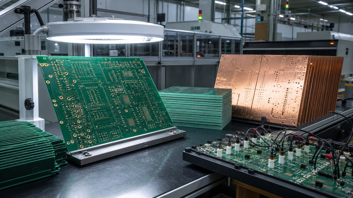
PCB fabrication inspection with finished circuit boards, copper panels and test fixture equipment
Electrical testing, visual inspection and process records help confirm that the fabricated boards match the approved design data.

Quality checks are also practical supplier filters. A fabricator that can explain test equipment, inspection points and process records is usually easier to work with than one that only quotes a low price. Best Technology’s PCB test equipment page is a useful internal reference when a buyer wants to understand what inspection capability may be relevant.

Cost and Lead Time Factors in Custom PCB Fabrication

Custom PCB fabrication cost and lead time usually increase when the board needs more controlled process steps or less common material.

Important cost drivers include layer count, panel utilization, board thickness, copper weight, line width and spacing, hole count, smallest drill, blind or buried vias, surface finish, impedance control, special material, testing requirements, quantity and delivery speed. A small board is not always cheap if it requires HDI, heavy copper, tight drilling or special laminate. A larger board may be easier if it uses standard material and relaxed tolerances.

Buyers should ask suppliers to separate tooling, bare board fabrication, assembly, component sourcing, testing and shipping costs when the project includes more than the bare PCB. This prevents a low board price from hiding a high assembly or logistics risk.

Supplier Questions Before You Approve Fabrication

The best RFQ questions help the supplier expose manufacturing risk before the board enters production.

  • Are any traces, spaces, holes or annular rings outside standard capability?
  • Is the requested material in stock, or does it require special sourcing?
  • Does the stackup support the required impedance and finished thickness?
  • Is the selected surface finish suitable for the component packages and storage time?
  • Are there any panelization issues that could affect assembly or depaneling?
  • Which tests are included, and which reports require an extra request?
  • What design change would reduce cost, lead time or yield risk?

If the design falls outside standard FR4 or routine multilayer production, a special PCB review can help clarify whether the project needs heavy copper, high-frequency material, metal core, ceramic, rigid-flex or another custom process path.

FAQ

What files are required for custom PCB board fabrication?

Most fabrication orders need Gerber or ODB++ files, NC drill files, board outline, stackup, copper weight, thickness, material, solder mask, legend, surface finish and any special tolerance notes. A fabrication drawing is useful when dimensions, impedance, controlled-depth drilling or acceptance criteria matter.

Is PCB fabrication the same as PCB assembly?

No. PCB fabrication makes the bare printed circuit board. PCB assembly places and solders components onto that board. A turnkey PCBA project needs both steps, plus BOM review, component sourcing, stencil planning, inspection and testing.

What makes a custom PCB harder to fabricate?

HDI microvias, blind or buried vias, heavy copper, tight spacing, unusual thickness, special materials, controlled impedance, fine-pitch solder mask, large panels and strict inspection requirements can all increase fabrication difficulty.

Which surface finish should I choose?

The right finish depends on assembly method, component package, shelf life, flatness and cost. ENIG is often chosen for fine pitch and flatness, HASL can fit less demanding boards, and OSP may fit some cost-sensitive builds. Confirm with the assembler before ordering.

How can I reduce PCB fabrication cost?

Use standard material when possible, improve panel utilization, avoid unnecessary tight tolerances, simplify via structures, keep copper weight realistic, choose a suitable finish and send complete files. Do not remove inspection that protects product reliability.

Can a fabricator fix my PCB design files?

A fabricator can often flag manufacturability issues and suggest changes, but it should not silently change electrical intent. Any change to spacing, pad shape, drill size, stackup or material should be reviewed and approved by the design owner.

When should I request impedance control?

Request impedance control when the board carries high-speed digital, RF, differential pairs, antennas or other signals that depend on trace geometry and dielectric structure. Provide target impedance, tolerance, reference layers and stackup requirements.

Does custom PCB fabrication always take longer than standard PCB orders?

Not always. A custom board with standard FR4, clean files and routine tolerances can move quickly. Lead time increases when the design needs special material, complex stackup, extra testing, unusual finish or unresolved DFM clarification.

Final Thoughts

Custom PCB board fabrication is predictable when the design files, stackup, material choices, process limits and inspection requirements are clear before production. The safest RFQ is not the one with the fewest details. It is the one that lets the supplier identify cost, lead time and yield risk before the first panel is built.

If you are preparing a custom PCB for prototype or production, send your Gerber, drill, stackup, BOM and assembly files to the Best Technology engineering team at sales@bestpcbs.com for fabrication, PCBA and quotation review.

You may also like

Custom PCB Manufacturing Lead Time
Saturday, July 11th, 2026
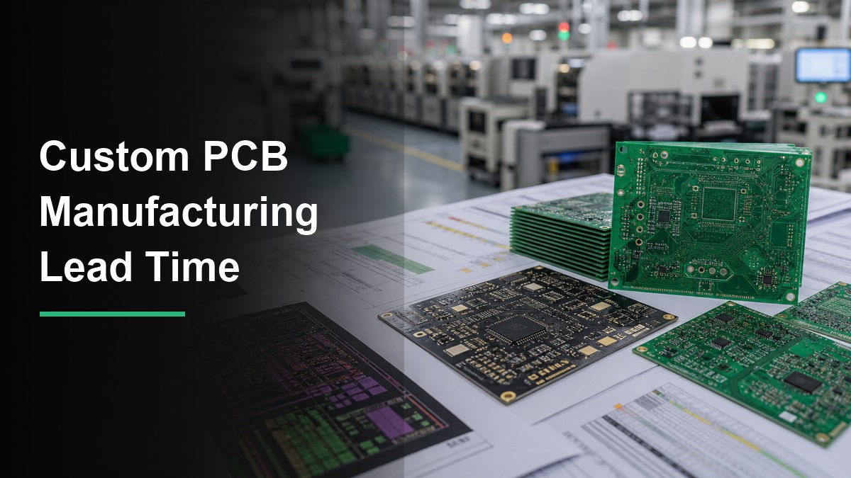
Custom PCB manufacturing lead time planning with PCB boards and production documents
Custom PCB lead time is easier to control when design files, materials, production steps and inspection needs are reviewed before quotation.

Custom PCB manufacturing lead time is the time from approved production files and quote confirmation to finished boards or assembled PCBAs ready for shipment. It is not set only by layer count. File quality, material availability, surface finish, copper weight, impedance control, component sourcing, testing scope, production queue and shipping route can all add or remove days.

For buyers, the practical question is not “what is the fastest possible PCB lead time?” The better question is “what information does the factory need to confirm a reliable lead time for this exact board?” A simple FR4 prototype with complete Gerbers can move quickly. A custom PCB with HDI, controlled impedance, special laminate, heavy copper, tight drilling, turnkey assembly or functional testing needs a more careful schedule.

What Counts as Custom PCB Manufacturing Lead Time?

Custom PCB manufacturing lead time should be counted after the supplier has approved the production data, confirmed materials and accepted the order, not from the first email.

A realistic timeline usually includes engineering review, quotation clarification, material preparation, bare board fabrication, surface finish, electrical test, optional assembly, final inspection, packing and logistics. If the project includes turnkey PCBA, component sourcing and incoming parts inspection must be counted separately from bare PCB fabrication.

This is why two boards with the same layer count can have different schedules. A standard 4-layer FR4 board with common finish may be simple. A similar-looking 4-layer board with unusual thickness, special copper, impedance coupons, tight annular rings, press-fit connectors or high-reliability testing may need more review and queue time.

Typical Lead Time Stages Buyers Should Separate

The most useful lead time estimate separates engineering review, PCB fabrication, assembly, testing and shipping instead of giving one vague number.

Stage What Happens Common Delay Trigger Buyer Action
Engineering review Gerber, drill, stackup, drawing, BOM and assembly data are checked. Missing notes, unclear tolerances, mismatched drill files or incomplete BOM. Send a complete file package and answer DFM questions quickly.
Material preparation Laminate, copper, prepreg, solder mask and components are reserved. Special laminate, high Tg, RF material, ceramic substrate or allocated components. Approve alternates early and confirm critical material rules.
PCB fabrication Imaging, etching, lamination, drilling, plating, solder mask and finish are completed. HDI, buried vias, thick copper, tight spacing, unusual finish or panel constraints. Keep the first build inside standard capability when schedule matters.
PCBA assembly Stencil, SMT placement, reflow, through-hole work, cleaning and inspection are performed. Long-lead components, BGA/X-ray needs, mixed SMT/THT, fixture setup or programming. Confirm BOM availability and provide placement, polarity and test notes.
Inspection and logistics AOI, electrical test, visual inspection, packing and shipment are arranged. Extra test reports, rework, customs documents or remote shipping destination. Define required reports and shipping method before production starts.

Files That Shorten or Delay a Custom PCB Schedule

Complete files shorten lead time because the factory can quote, review and release production without repeated clarification.

For bare PCB fabrication, send Gerber or ODB++ files, NC drill files, board outline, stackup requirement, copper weight, board thickness, solder mask color, silkscreen color, surface finish, impedance notes, controlled-depth drilling notes and any special acceptance criteria. For PCBA, add BOM, centroid or pick-and-place file, assembly drawing, polarity notes, firmware or programming instructions, and test requirements.

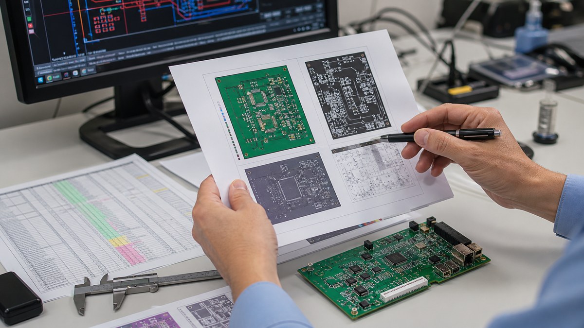
Engineer reviewing PCB files before confirming custom PCB lead time
Incomplete Gerber, BOM, stackup or assembly notes can turn a quick-turn request into a clarification loop.

A common delay is a file set that looks complete but has contradictions. Examples include a board outline that does not match the mechanical drawing, a BOM package that does not match the centroid file, a stackup note that conflicts with impedance requirements, or a surface finish choice that is not suitable for the component package. These issues should be solved before the purchase order is treated as production-ready.

Board Complexity Has More Impact Than Board Size Alone

Lead time usually increases when the board requires more controlled process steps, tighter inspection or less common materials.

Layer count matters, but it is only one part of the schedule. HDI microvias, blind or buried vias, sequential lamination, heavy copper, fine line and space, controlled impedance, unusual thickness, rigid-flex construction and special surface finishes can all add review and production time. If a project needs HDI density, review the board against realistic HDI PCB manufacturing limits before asking for rush delivery.

Material choice also matters. Standard FR4 is usually easier to schedule than a special laminate, ceramic substrate, metal core PCB, RF material or high-temperature stackup. If standard FR4 is acceptable, the FR4 printed circuit board route may reduce sourcing risk. If the design needs special thermal, high-frequency or structural behavior, lead time should include material confirmation.

PCBA Lead Time Depends on Components, Not Only Assembly Speed

For turnkey PCBA, component availability often controls the real delivery date more than placement speed.

A factory may be able to assemble a small batch quickly once all parts are ready, but that does not mean every assembled board can ship quickly. Long-lead ICs, connectors, magnetics, sensors, relays, custom cables, displays and odd passives can delay the start of assembly. If the BOM has obsolete, allocated or region-specific parts, schedule risk should be discussed before the order is placed.

When schedule matters, confirm whether the supplier can support component sourcing, approved alternates, incoming inspection and shortage reporting. A practical BOM review should identify no-stock items, risky single-source parts, package mismatches and parts that require programming or special handling.

When Quick-Turn PCB Manufacturing Is Realistic

Quick-turn service is realistic when the design uses available materials, complete files and a process flow that fits the factory queue.

Fast schedules work best for simple prototypes, standard materials, small or medium panel sizes, common finishes, clean drill data, no unresolved DFM issues and components that are already in stock. A quick-turn request becomes less reliable when the board needs special laminate, multiple lamination cycles, unusual solder mask, tight impedance tolerance, large panels, heavy copper, fixture-based testing or long-lead components.

For assembled prototypes, a dedicated prototype PCB assembly flow can help engineering teams validate a design before locking mass production. If the project must move from prototypes into larger volumes, quick turn PCB assembly should be planned with component supply and test coverage in mind.

Rush Fees Do Not Fix Every Lead Time Problem

Expedited service can compress queue time, but it cannot remove engineering, material or component constraints that still need resolution.

Rush delivery is most useful when the files are clean and the process is standard. It is less useful when the supplier still needs to clarify impedance, stackup, plating, tolerances, test methods, part substitutions or acceptance criteria. Paying for speed before the file package is stable can create rework rather than faster delivery.

A better approach is to ask the supplier which step controls the schedule. If the answer is material sourcing, choose an available material or accept a longer lead time. If the answer is DFM risk, revise the design. If the answer is component shortage, approve alternates or split the build. If the answer is production queue, expedited service may help.

How to Prepare an RFQ for a Reliable Lead Time

A lead-time-ready RFQ should let the supplier quote the board without guessing about design intent, assembly scope or acceptance criteria.

  • Send the final Gerber or ODB++ package, NC drill files and board outline.
  • Include stackup, copper weight, board thickness, material preference and surface finish.
  • Mark impedance, controlled-depth drilling, press-fit holes, castellations or edge plating if used.
  • For PCBA, send BOM, centroid file, assembly drawing, polarity notes and testing requirements.
  • State the target quantity, prototype or production purpose, required delivery date and shipping country.
  • List any parts that cannot be substituted and any parts where alternates are allowed.
  • Ask the supplier to separate fabrication, component sourcing, assembly, testing and shipping time.

Lead Time Risk Checklist Before You Approve Production

Before approval, check the schedule against the real manufacturing risks instead of accepting a single optimistic delivery date.

PCB assembly production line reviewing schedule before shipment
Production lead time should include fabrication, assembly, inspection, packing and logistics, not only machine time.
  • Are all production files approved and version-controlled?
  • Are laminate, copper, solder mask and surface finish available?
  • Do all critical components have stock, alternates or confirmed purchase dates?
  • Does the board need impedance testing, flying probe, fixture test, AOI, X-ray or functional test?
  • Does the first article require engineering approval before the full batch continues?
  • Are packaging, labeling, customs documents and shipping method already defined?
  • Is the promised date based on working days, calendar days or shipment date?

How to Reduce Custom PCB Manufacturing Lead Time Without Raising Risk

The safest way to reduce lead time is to remove uncertainty before production starts.

Use standard materials when possible, keep the first prototype inside common capability, avoid unnecessary special finishes, release a clean BOM, allow qualified alternates and answer DFM questions fast. For PCBA, order critical long-lead components early or let the supplier source parts before the bare boards are finished. For repeat builds, keep the same approved stackup, finish, stencil and test plan unless a change is necessary.

Do not shorten lead time by skipping review on a high-risk board. A missed annular ring issue, wrong footprint, unavailable connector or unclear test requirement can cost more time than a proper review. Good suppliers should be willing to explain the bottleneck instead of only quoting the fastest possible date.

Supplier Questions That Reveal Whether the Schedule Is Reliable

Ask schedule questions that force the supplier to show where the lead time comes from.

  • When does your lead time clock start: quote approval, payment, file approval or material arrival?
  • Which step is the current bottleneck for this board?
  • Are the laminate, solder mask, surface finish chemicals and critical components already available?
  • What changes would shorten the lead time without weakening reliability?
  • Does the quote include electrical test, AOI, X-ray, functional test or only basic inspection?
  • Will the promised date be shipment date or arrival date?
  • What happens if DFM review finds a file issue after order approval?

FAQ About Custom PCB Manufacturing Lead Time

These answers are written for buyers preparing an RFQ, not for one fixed factory schedule.

How long does custom PCB manufacturing take?

It depends on board complexity, material availability and whether assembly is included. Simple prototypes can move much faster than HDI, rigid-flex, ceramic, heavy copper or fully assembled PCBAs. Treat any published number as a starting point and ask for a quote based on your actual files.

When should I start counting PCB lead time?

Count lead time after production files are approved, the order is confirmed and required materials or components are available. Early emails, incomplete Gerbers or unresolved BOM questions should not be treated as production time.

What files are needed to confirm custom PCB lead time?

For bare boards, send Gerber or ODB++ files, drill files, board outline, stackup, material, thickness, copper weight and finish. For PCBA, add BOM, centroid file, assembly drawing, polarity notes and test requirements.

Does PCBA always add more lead time than bare PCB fabrication?

Usually yes, because assembly needs stencil preparation, component sourcing, placement, soldering, inspection and sometimes testing. The largest delay is often component availability, not the placement process itself.

Can I reduce lead time by using standard FR4?

Often yes. Standard FR4, common board thickness, common copper weight and common surface finish are easier to schedule than special laminate, ceramic, RF material, metal core, rigid-flex or unusual process requirements.

What makes HDI or rigid-flex boards slower?

HDI and rigid-flex designs may need sequential lamination, laser drilling, tighter registration, controlled impedance, special materials and extra inspection. These steps are useful, but they should be planned instead of treated like standard quick-turn FR4 work.

Do rush fees guarantee delivery?

No. Rush fees may reduce queue time, but they cannot remove material shortages, unresolved DFM issues, unavailable components or unclear test requirements. Ask which step controls the schedule before approving an expedite charge.

How can I avoid delays after placing the order?

Freeze the file revision, respond to DFM questions quickly, approve part alternates early, confirm test requirements and avoid changing quantity, finish or shipping method after production starts.

Should I split prototypes and production into separate orders?

For new designs, yes in many cases. A prototype order can validate the layout, BOM, assembly process and test plan before a larger production batch. This reduces the risk of repeating an error at volume.

What should a supplier include in a clear lead time quote?

The quote should separate engineering review, material or component sourcing, bare PCB fabrication, assembly, inspection, packing and shipping. It should also state whether the date means completion, shipment or delivery.

Final Buying Advice

Custom PCB manufacturing lead time is predictable when the supplier sees the full design, confirms materials and separates each production stage. Before approving a rush order, ask what is slowing the schedule and whether a file, material or BOM change would reduce risk. If you are planning PCB fabrication, turnkey PCBA, prototypes or mass production, send your Gerber, BOM and assembly files to the Best Technology engineering team at sales@bestpcbs.com for a lead time and quotation review.

You may also like

Ceramic PCB Prototype Production Guide: Process, Materials and RFQ Tips
Friday, July 10th, 2026

ceramic pcb prototype production is the controlled sample-building stage used to verify a ceramic circuit design before volume manufacturing. It helps engineers confirm substrate choice, copper pattern, thermal path, tolerances, assembly risk, and test requirements before committing to production tooling or a larger order.

For buyers and hardware teams, a ceramic PCB prototype is not just a small quantity of boards. It is a practical engineering checkpoint for high-power LEDs, power modules, sensors, RF designs, automotive electronics, medical devices, and other circuits where heat, dimensional stability, insulation, or reliability can decide whether the final product works.

What Is Ceramic PCB Prototype Production?

Ceramic PCB prototype production is the first manufacturing run of a ceramic circuit board design, usually built to validate the material, copper layout, process route, inspection plan, and assembly compatibility. The goal is to find manufacturability issues while the design can still be corrected without large production losses.

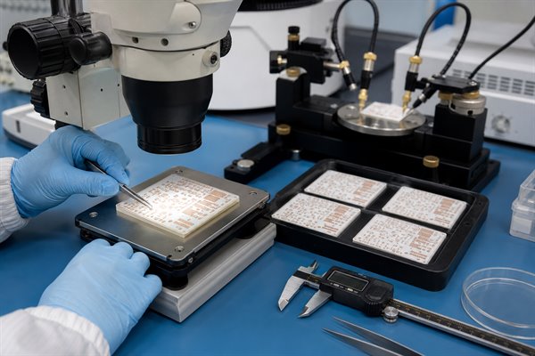
Ceramic PCB prototype production scene with ceramic circuit samples under microscope inspection

Unlike a standard FR4 prototype, a ceramic prototype depends heavily on substrate behavior, metallization method, firing or bonding process, conductor adhesion, surface flatness, and thermal expansion matching. A good prototype order should therefore answer both electrical and manufacturing questions, not only confirm that the Gerber files can be plotted.

For a new project, the prototype stage often confirms whether ceramic PCB technology is the right direction, or whether an alternative such as FR4 PCB or metal-core PCB is enough for the thermal and cost target.

Why Is Ceramic PCB Prototyping Different from FR4 PCB Prototyping?

Ceramic PCB prototyping is different because the substrate is rigid, hard, thermally conductive, and much less forgiving than glass-reinforced epoxy laminate. The process needs more attention to ceramic material selection, copper bonding, drilling or laser processing, dimensional tolerance, and thermal cycling behavior.

Prototype factor FR4 PCB prototype Ceramic PCB prototype
Base material Glass epoxy laminate Al2O3, AlN, BeO alternatives, LTCC, HTCC, or other ceramic substrates
Main design concern Signal routing, layer stack, cost, and standard fabrication limits Thermal path, ceramic thickness, copper adhesion, CTE match, and process route
Mechanical behavior Can flex slightly before fracture Brittle and requires careful handling, panel design, and fixture planning
Prototype review focus DFM, impedance, hole quality, solder mask, assembly fit Metallization quality, substrate flatness, thermal design, edge quality, and inspection plan

This difference affects the RFQ stage. A supplier should review not only the Gerber data, but also the ceramic material, copper thickness, board outline, via structure, tolerance needs, component heat load, and whether the prototype must support later mass production approval.

Which Ceramic PCB Material Should You Choose for a Prototype?

The best ceramic prototype material depends on thermal conductivity, insulation requirement, mechanical strength, cost target, and the final application environment. Al2O3 is commonly chosen for cost-effective ceramic prototypes, while AlN is often selected when higher thermal conductivity is required.

Material or technology Why it is used in prototypes Typical review point
Al2O3 ceramic Balanced cost, insulation, mechanical stability, and mature processing Check whether thermal performance is enough for the heat load
AlN ceramic Higher thermal conductivity for power and LED designs Confirm cost, availability, and metallization compatibility
Thick film ceramic Useful for printed conductor, resistor, and hybrid circuit structures Review conductor geometry and fired pattern tolerance
Thin film ceramic Used where fine lines, stable circuits, or precise patterns are needed Confirm line width, adhesion, finish, and application fit
DPC, DCB, or related structures Selected when copper thickness, thermal path, or power handling drives the design Match the process route to copper thickness and reliability needs

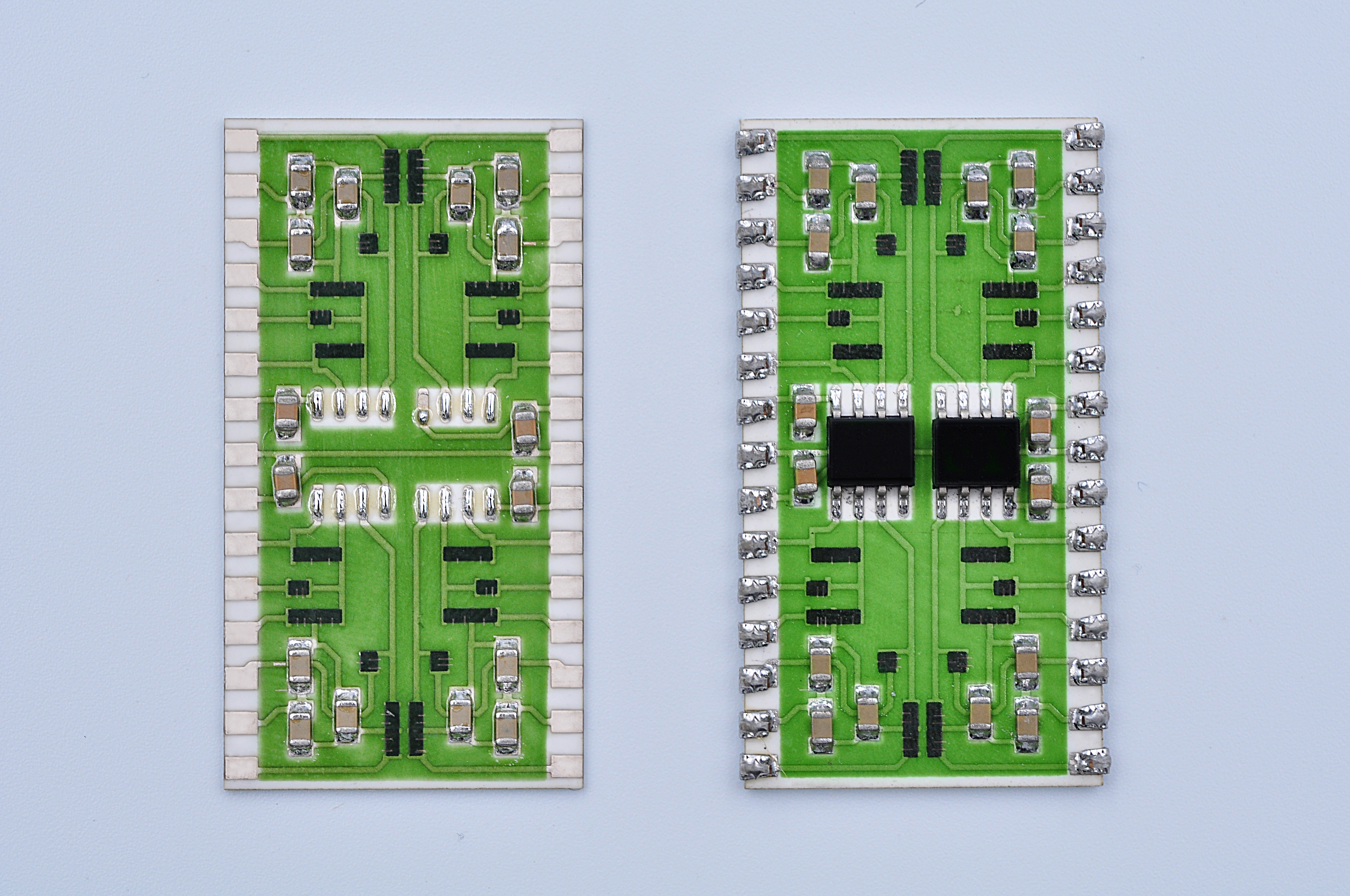
If the project is still early, ask the manufacturer to compare available ceramic options before confirming the prototype route. EBest Circuit supports ceramic PCB categories such as thick film ceramic PCB, thin film ceramic PCB, DPC ceramic PCB, and DCB ceramic PCB, so the prototype can be planned around the final production requirement instead of treated as an isolated sample.

What Is the Ceramic PCB Manufacturing Process?

The ceramic PCB manufacturing process usually starts with design review and material selection, then moves through substrate preparation, metallization, patterning, firing or bonding, surface finish, profiling, inspection, testing, and packing. The exact route depends on whether the project uses thick film, thin film, DPC, DCB, LTCC, HTCC, or another ceramic process.

Ceramic PCB prototype manufacturing process samples arranged from substrate to copper patterned board
  1. Engineering review: Check Gerber files, drill data, board outline, copper thickness, substrate thickness, tolerances, and application requirements.
  2. Material preparation: Select Al2O3, AlN, or another ceramic substrate and confirm thickness, size, flatness, and handling needs.
  3. Metallization and patterning: Build the conductive layer using the selected process route, then define circuit features according to the design.
  4. Thermal or bonding process: Fire, sinter, plate, bond, or otherwise stabilize the conductor system depending on the technology.
  5. Finishing and profiling: Apply the required surface finish, cut the outline, and prepare the board for inspection or assembly.
  6. Inspection and test: Review dimensions, conductor quality, insulation, open/short status, surface quality, and packaging condition.

A prototype should be reviewed as a process sample. If the prototype later moves into production, the same data package, material choice, and inspection criteria should be stable enough to repeat.

How Do Thick Film, Thin Film, DPC and DCB Affect Prototype Production?

Different ceramic PCB process routes affect prototype cost, minimum features, copper thickness, thermal performance, and sample lead time. Choosing the process too late can force the engineering team to redesign pads, traces, vias, or thermal areas after the first prototype.

Thick film ceramic PCB is often used for hybrid circuits and printed conductor structures. It can be practical for prototypes where fired pastes, resistive elements, or ceramic-based circuit patterns are part of the design.

Thin film ceramic PCB is better suited for finer features and stable circuit requirements. It is often reviewed for sensor, microwave, medical, and precision electronic applications where conductor geometry matters.

DPC and DCB ceramic PCB routes are more closely tied to power electronics and heat transfer. For these prototypes, copper thickness, adhesion, thermal cycling, and substrate-to-copper reliability need early review.

What Files Are Needed for a Ceramic PCB Prototype Quote?

A ceramic PCB prototype quote is more accurate when the supplier receives a complete technical package, not just a screenshot or partial Gerber export. Missing tolerances, material notes, and assembly requirements can cause delays or a quote that does not match the real production risk.

  • Gerber files and drill data
  • Board outline drawing with critical dimensions
  • Ceramic material preference, such as Al2O3 or AlN
  • Substrate thickness and copper thickness requirement
  • Surface finish requirement
  • Panelization or single-piece delivery preference
  • Quantity for prototype and expected production volume
  • Assembly files if the prototype needs PCBA service
  • Thermal, electrical, or reliability test requirements
  • Application notes, especially for high-power, high-temperature, LED, sensor, or RF use

When a buyer provides both the prototype quantity and the expected mass production target, the manufacturer can recommend a route that avoids sample-only shortcuts that may not scale.

What Should You Check Before Moving from Prototype to Production?

Before moving from ceramic prototype to production, check whether the prototype truly validates the final design, process, material, and inspection standard. A board that passes a simple electrical test may still need thermal, mechanical, and assembly review before mass production.

Ceramic PCB prototype inspection under microscope with caliper and probe station in quality lab
  • Confirm the ceramic material and thickness match the final thermal design.
  • Check conductor adhesion, line quality, edge quality, and surface finish.
  • Review substrate flatness and dimensional tolerance against assembly needs.
  • Test open/short status, insulation resistance, and critical electrical paths.
  • Review solderability or bonding compatibility if components will be mounted.
  • Record any design changes before approving the production file set.
  • Ask whether the same process route will be used for the production batch.

The cleanest transition happens when the prototype report, customer feedback, corrected files, and final production requirements are all connected before the next purchase order.

What Problems Can Delay Ceramic PCB Prototype Production?

Ceramic PCB prototype production is often delayed by incomplete files, unclear material selection, unrealistic tolerances, process-route mismatch, missing assembly data, or late changes to the thermal design. These problems are easier to fix before production starts than after substrates and tooling have been prepared.

Delay cause Why it matters How to prevent it
Unclear ceramic material Al2O3, AlN, and other ceramics change cost and thermal behavior Share heat load, application, and target cost before quoting
Missing tolerance drawing Ceramic processing may need different tolerance planning than FR4 Mark critical dimensions and non-critical dimensions separately
Wrong process route Thick film, thin film, DPC, and DCB do not fit the same designs equally Ask the supplier to review process fit before sample build
Late assembly requirement Pad finish, flatness, and component heat transfer may need early planning Send BOM, placement file, and assembly notes with the RFQ

How to Choose a Ceramic PCB Prototype Manufacturer?

Choose a ceramic PCB prototype manufacturer by checking whether the supplier can review material selection, process route, DFM risk, inspection requirements, assembly needs, and future production scaling. Price matters, but the cheapest sample is not useful if the process cannot support the final product.

Good supplier questions include:

  • Which ceramic materials and process routes are suitable for this design?
  • Can the same route support prototype and mass production?
  • What design features may increase cost or delay?
  • Which tolerances should be relaxed if they are not functional?
  • What tests are recommended for this application?
  • Can assembly, inspection, and packaging be coordinated in one project flow?

EBest Circuit can support custom ceramic PCB projects from prototype review to sample production and later batch manufacturing. For projects that need assembled samples, prototype PCB fabrication can also be coordinated with PCBA review to reduce handoff risk.

FAQ

How much does a ceramic PCB prototype cost?

Ceramic PCB prototype cost depends on material, substrate thickness, copper thickness, process route, dimensions, tolerance level, quantity, surface finish, testing, and whether assembly is included. Al2O3 prototypes are often more cost-effective than higher thermal conductivity ceramic options, but the right choice should be based on the heat load and reliability target.

Can ceramic PCB prototypes be assembled?

Yes, ceramic PCB prototypes can be assembled when the pad finish, flatness, component package, soldering or bonding method, and thermal requirements are reviewed early. If assembly is needed, send the BOM, placement file, polarity notes, and any thermal interface requirements with the PCB quotation package.

Is Al2O3 or AlN better for ceramic PCB prototype production?

Al2O3 is often selected for balanced cost and mature processing, while AlN is chosen when higher thermal conductivity is required. The better option depends on the heat source, insulation requirement, mechanical design, available budget, and whether the prototype must represent a later production build.

Can one ceramic PCB prototype be used for mass production approval?

One prototype can support production approval only if it uses the same material, process route, design file set, tolerance standard, inspection method, and assembly assumptions planned for mass production. If the prototype used sample-only changes, a second verification run may be needed before release.

What tolerances matter most in ceramic PCB prototyping?

The most important tolerances are usually board outline, hole or slot position, substrate thickness, copper feature size, registration, flatness, and critical pad locations. The buyer should identify which dimensions affect assembly or function, because unnecessary tight tolerances can increase cost and delay without improving performance.

What is the difference between ceramic prototype and ceramic PCB prototype?

A ceramic prototype can refer to any trial part made from ceramic material, while a ceramic PCB prototype is a circuit board sample built on a ceramic substrate with conductive patterns for electronic use. For RFQ clarity, use ceramic PCB prototype when the part includes circuit fabrication requirements.

How Can EBest Circuit Support Ceramic PCB Prototype Production?

EBest Circuit supports ceramic PCB prototype production by helping buyers review materials, process route, manufacturability, inspection needs, and assembly requirements before moving into larger production. If you are developing a ceramic PCB for LED, power electronics, sensor, automotive, medical, or industrial electronics applications, send your files and requirements to the engineering team for a practical review and quotation at sales@bestpcbs.com.

You may also like

HDI PCB Fabrication Guide: Stackups, Microvias, Process, and Cost
Friday, July 10th, 2026

Smaller components and finer-pitch packages have changed how engineers route multilayer PCBs. A conventional through-hole structure may work well for a 0.8 mm-pitch BGA, but it often becomes restrictive once the pitch drops to 0.5 mm, 0.4 mm, or below.

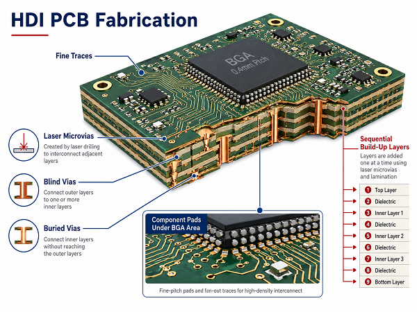
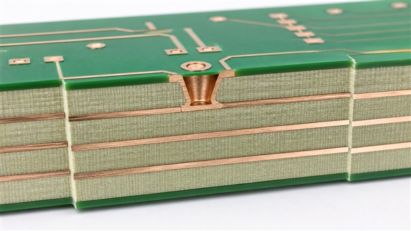
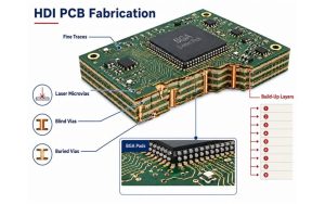
That is where HDI PCB fabrication becomes useful. A high-density interconnect PCB uses microvias, thin dielectric layers, smaller pads, and sequential lamination to create more routing channels within a limited area. It also adds laser drilling, via filling, tighter registration, and additional lamination work.

What Is HDI PCB Fabrication?

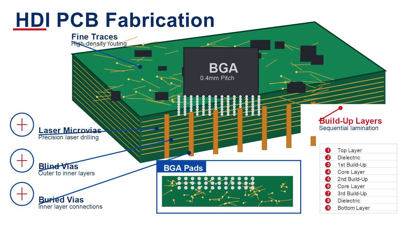
HDI PCB fabrication is the manufacture of printed circuit boards with a higher wiring density than standard multilayer boards. Common HDI features include:

  • Laser-drilled microvias
  • Blind and buried vias
  • Fine trace and space
  • Small capture pads
  • Thin dielectric layers
  • Via-in-pad structures
  • Sequential lamination
  • Stacked or staggered microvias

HDI is useful when a design must escape signals from a fine-pitch BGA, reduce board size, shorten interconnections, or increase routing density without adding an excessive number of layers.

It is often unnecessary when the PCB has enough routing space, uses larger-pitch packages, and can be completed with standard through-holes. In that case, a conventional multilayer PCB is usually more economical.

HDI PCB Fabrication

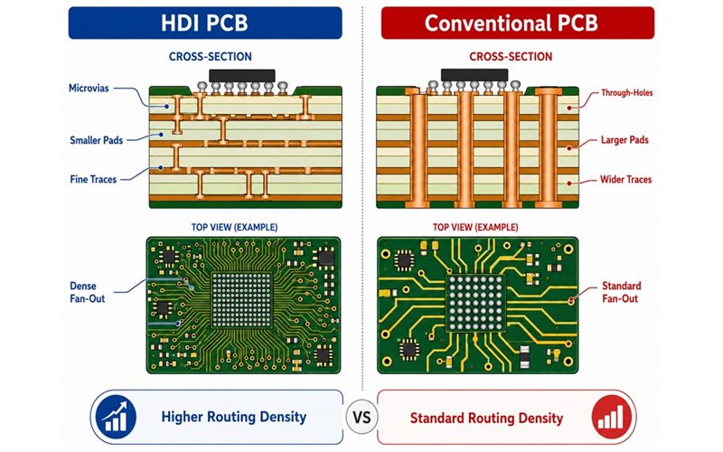
How Is an HDI PCB Different from a Conventional Multilayer PCB?

Both are multilayer PCBs, but their interconnection methods and production routes are different.

Design factor Conventional multilayer PCB HDI PCB
Main via type Mechanically drilled through-hole Laser microvia, blind via, and buried via
Via depth Usually passes through the complete board Usually connects adjacent build-up layers
Lamination Mainly one multilayer lamination sequence One or more sequential build-up cycles
Pad size Relatively large Smaller capture and target pads
Fine-pitch BGA routing More restricted Better suited to dense fan-out
Manufacturing cost Lower for standard layouts Higher because of added processing
Main benefit Simpler and economical Higher routing density and smaller size

A standard multilayer PCB remains the better option when routing can be completed without microvias. HDI becomes worthwhile when through-hole pads block routing channels or force an unnecessary increase in board size or layer count.

Comparison between HDI PCB and conventional multilayer PCB structures and BGA fan-out density

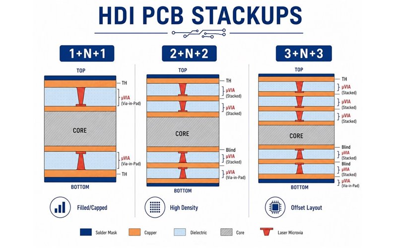
What Are the Main Types of HDI PCB Stackups?

HDI stackups are commonly described as 1+N+1, 2+N+2, or 3+N+3. The outer numbers show the number of HDI build-up layers on each side. 鈥淣鈥?represents the central core structure.

HDI stackup Construction Typical use
1+N+1 One build-up layer on each side Moderate-density BGAs, industrial controls, and consumer products
2+N+2 Two build-up layers on each side Dense processors, communication modules, and medical electronics
3+N+3 Three build-up layers on each side Advanced computing and highly compact electronics
Any-layer HDI Microvias between many adjacent layers Highly miniaturized products and complex modules
Asymmetric HDI Different build-up structures on each side Boards with density concentrated on one surface

A 1+N+1 construction is usually the most economical HDI entry point. Moving to 2+N+2 or 3+N+3 should be driven by actual routing needs because every additional build-up level adds process steps and registration interfaces.

HDI PCB stackup comparison showing 1 plus N plus 1, 2 plus N plus 2, and 3 plus N plus 3 constructions

What Types of Vias Are Used in High-Density Interconnect PCBs?

An HDI board usually combines several via types rather than using microvias everywhere.

  • Plated through-hole: Connects the full board thickness and is often used for connectors, power, and component leads.
  • Blind via: Connects an outer layer to one or more inner layers without passing through the complete PCB.
  • Buried via: Connects internal layers and is not visible from the surface.
  • Laser microvia: A small blind via used for fine-pitch routing.
  • Via-in-pad microvia: Located directly inside a component pad, commonly beneath BGAs.
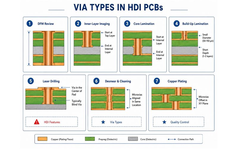
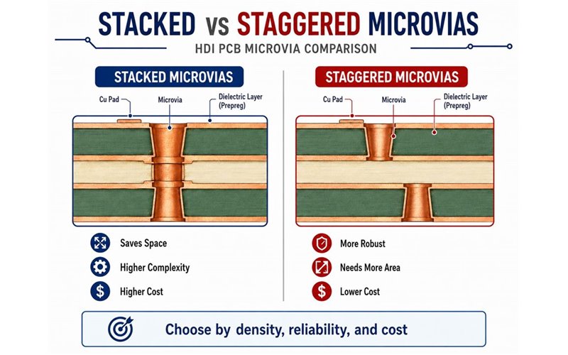
  • Staggered microvia: Microvias on adjacent levels are laterally offset.
  • Stacked microvia: Two or more microvias are aligned vertically.
  • Skip microvia: Connects non-adjacent layers through more than one dielectric layer.

Large mechanically drilled vias may still be better for high current, connector strength, and thermal transfer. The via architecture should follow the electrical and routing requirements, not a desire to use the most advanced-looking structure.

Cross-section illustrations of via structures used in high-density interconnect printed circuit boards

How Does the HDI PCB Manufacturing Process Work?

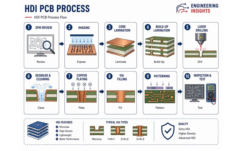
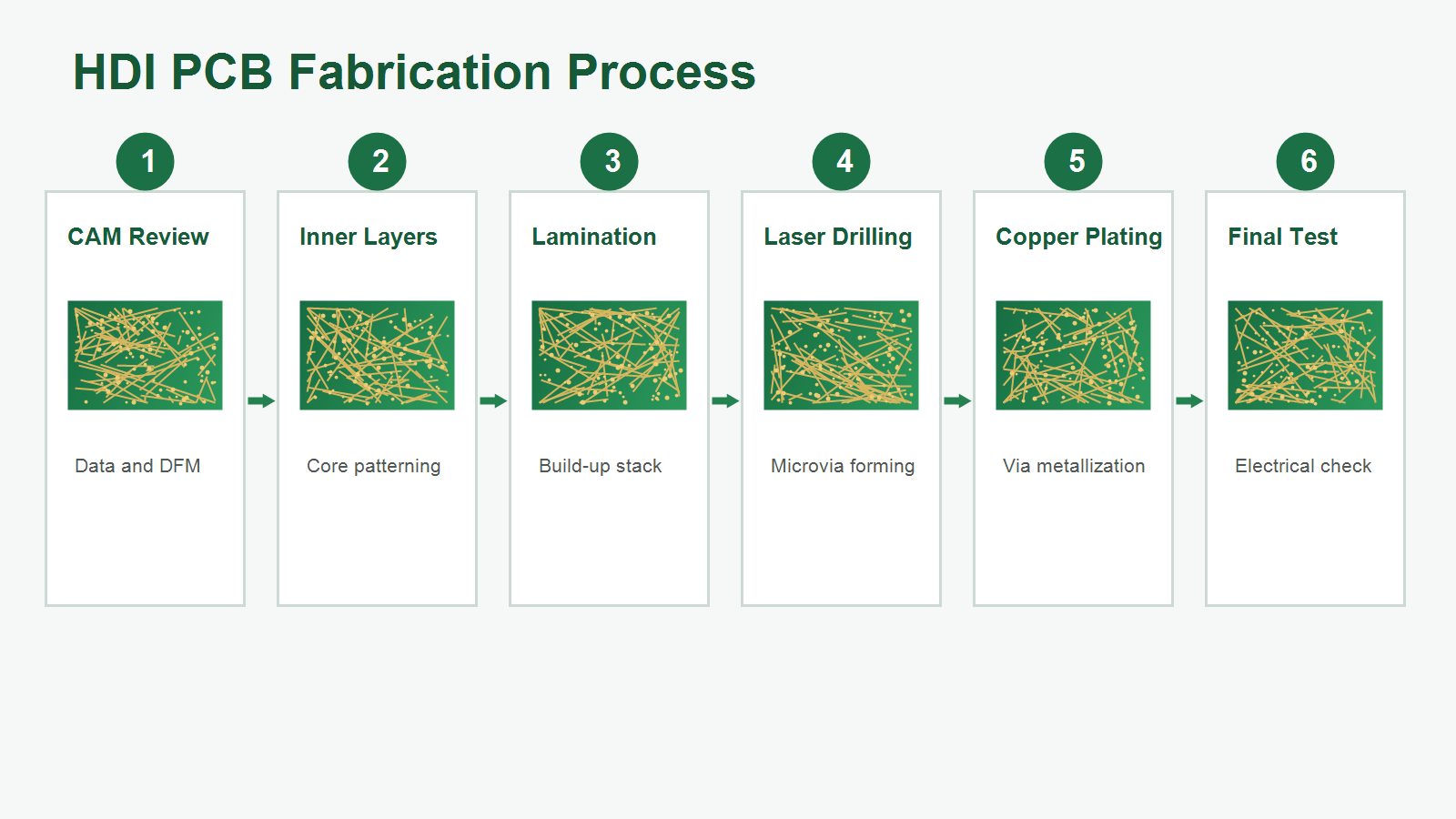
The exact HDI PCB manufacturing process depends on the stackup and microvia architecture. A typical route includes:

  1. DFM and stackup review: Confirm materials, dielectric thickness, microvia geometry, impedance, and copper weight.
  2. Inner-layer imaging and etching: Form and inspect the internal copper circuits.
  3. Buried-via processing: Drill, clean, plate, and inspect buried vias where required.
  4. Core lamination: Press the internal layers and prepreg into the central multilayer structure.
  5. Build-up lamination: Add thin dielectric and copper layers to the core.
  6. Laser drilling: Form controlled blind microvias.
  7. Desmear and cleaning: Remove laser residue and expose the target pads.
  8. Copper deposition and plating: Metallize the microvia walls and build the required copper thickness.
  9. Via filling and planarization: Fill via-in-pad and stacked microvias and level the surface.
  10. Repeated build-up processing: Repeat lamination, drilling, and plating for additional HDI levels.
  11. Final board processing: Complete through-holes, solder mask, surface finish, profiling, and legend.
  12. Inspection and test: Perform AOI, electrical testing, impedance testing, X-ray inspection, and microsection analysis as required.

The drill table, stackup, fabrication drawing, and layer files must show the same via start and stop layers. Conflicting data delays engineering review and can lead to an incorrect production route.

HDI PCB manufacturing process from DFM review and imaging to laser drilling, plating, via filling, patterning, and testing

Why Is Sequential Lamination Required in HDI PCB Fabrication?

Sequential lamination is required because each microvia level is built in stages. In a 2+N+2 structure, the core is produced first, followed by the first build-up layer and its microvias. A second dielectric is then laminated over that surface before the next microvia level is drilled.

When stacked microvias are used, the lower microvia usually needs to be filled and planarized before the next microvia is placed above it.

Each additional build-up level increases:

  • Lamination cycles
  • Laser drilling operations
  • Plating and filling work
  • Registration requirements
  • Thermal exposure
  • Inspection requirements
  • Manufacturing cost

This is why moving from 1+N+1 to 2+N+2 can affect cost and lead time more than simply adding two conventional copper layers.

What Materials Are Used for HDI PCB Manufacturing?

Material selection should consider lamination cycles, z-axis expansion, signal loss, assembly temperature, and long-term reliability.

Material type Suitable use Main consideration
Standard FR-4 Cost-sensitive, moderate-density HDI May be less suitable for repeated high-temperature processing
High-Tg FR-4 Industrial, automotive, and multilamination HDI Improved thermal and dimensional stability
Low-CTE laminate Reliability-sensitive microvia structures Reduces expansion stress during thermal cycling
Low-loss laminate High-speed communication and computing Higher material and processing cost
Resin-coated copper Thin build-up layers Suitable for laser microvia formation
Build-up film Very fine HDI structures Requires specialized production capability
Halogen-free laminate Products with environmental material requirements Thermal and drilling performance must still be checked

High-Tg FR-4 is suitable for many industrial HDI boards. A low-loss material is justified only when insertion loss, data rate, rise time, or signal-integrity targets require it.

Do not approve a laminate substitution based on Tg alone. Also compare Dk, Df, z-axis CTE, decomposition temperature, CAF resistance, moisture absorption, copper adhesion, glass style, and resin content.

HDI PCB Design Guidelines

  • Confirm the stackup before routing. Dielectric thickness affects microvia depth, impedance, board thickness, and lamination.
  • Use microvias only where density requires them. Standard vias can remain in open areas.
  • Keep the microvia aspect ratio low. A depth-to-diameter ratio around 0.6:1 to 0.8:1 provides a wider manufacturing window.
  • Use the largest practical microvia and pad. Smaller geometry increases registration and plating risk.
  • Fill and cap solderable via-in-pad structures. Open vias beneath BGA pads can draw solder away from the joint.
  • Limit stacked microvia levels. More stacked interfaces increase process complexity and thermal stress.
  • Balance copper across the board. Uneven copper can affect resin flow, bow, twist, and plating.
  • Use the production stackup for impedance calculations. Include actual dielectric thickness, copper thickness, copper profile, and solder mask.
  • Keep drill definitions consistent. Every via group needs clear start and stop layers.
  • Provide test coupons when needed. Impedance, registration, and microvia coupons support process verification.

A useful rule is to use the largest feature that still completes the routing. Reducing geometry simply because the CAD tool allows it reduces fabrication margin without necessarily improving the product.

Stacked vs Staggered Microvias: Which Is Better?

Staggered microvias are usually preferred when enough lateral space is available. Stacked microvias are selected when routing density is more important than process simplicity.

Factor Staggered microvias Stacked microvias
Routing space Requires more lateral area Saves board area
Via filling Less demanding Lower vias normally need complete filling
Registration More forgiving Requires tighter vertical alignment
Process complexity Lower Higher
Cost Usually lower Usually higher
Reliability margin Generally wider More dependent on interface and plating quality
Best fit Industrial and reliability-sensitive products Dense BGA escape and compact electronics

Stacked microvias can be reliable when the lower vias are properly filled, planarized, aligned, and plated. For automotive, medical, aerospace, and long-life industrial products, staggered microvias are often the safer default unless layout density requires stacking.

Comparison of stacked and staggered microvias in an HDI PCB cross-section

What Common Defects Occur During HDI PCB Fabrication?

HDI defects are often internal, so visual inspection alone is not sufficient.

  • Microvia base separation: Weak connection between plated copper and the target pad.
  • Barrel or corner cracking: Related to thermal stress, copper ductility, or difficult geometry.
  • Plating voids: Incomplete copper coverage inside the microvia.
  • Incomplete via filling: Leaves a depression or internal void.
  • Excessive dimple: Creates an uneven via-in-pad surface.
  • Microvia misregistration: The drilled hole does not fully contact the target pad.
  • Resin voids or delamination: Caused by contamination, inadequate resin flow, or poor lamination control.
  • Fine-line opens or shorts: Linked to imaging, etching, or contamination issues.
  • CAF growth: Conductive paths develop through the laminate under moisture and electrical bias.
  • Bow and twist: Often related to asymmetric stackups or uneven copper distribution.

For reliability-sensitive boards, useful documentation can include microsection reports, impedance records, electrical test results, X-ray inspection, and thermal stress data.

What Factors Affect HDI PCB Fabrication Cost?

HDI cost is driven by process complexity, not only by layer count.

Cost factor Why it raises cost Practical control
Build-up levels More lamination and drilling cycles Use 1+N+1 where routing permits
Stacked microvias More filling, planarization, and alignment work Use staggered vias when space allows
Fine trace and space Reduces fabrication yield Restrict fine geometry to dense areas
Small microvias Tighter drilling and plating control Use larger geometry where possible
Via-in-pad quantity Adds filling and planarization Apply only where required
Specialized laminate Higher material cost and longer sourcing Use standard high-Tg FR-4 when suitable
Heavy copper Makes fine-line etching more difficult Separate high-current and fine-routing areas
Quick-turn schedule Requires priority engineering and processing Submit complete, approved files
Low quantity Setup cost is divided across fewer boards Use a production-compatible prototype design
Special testing Adds inspection and documentation Match testing to the end-use risk

Requesting a preliminary stackup before routing is one of the most effective cost controls. A well-planned 1+N+1 structure may replace a more expensive 2+N+2 design without affecting product performance.

Why Choose EBest Circuit for HDI PCB Fabrication?

HDI projects benefit from early communication between the customer and manufacturer. Stackup, microvia depth, filling method, material, impedance, and assembly requirements should be reviewed before final design release.

EBest Circuit, also known as Best Technology, supports HDI PCB fabrication from prototype review through PCB assembly and testing. Engineering discussions can cover:

  • 1+N+1 and 2+N+2 stackup planning
  • Laser microvia geometry
  • Stacked and staggered via selection
  • Via-in-pad filling and cap plating
  • High-Tg and low-loss materials
  • Controlled-impedance structures
  • Fine-pitch BGA fan-out
  • PCB assembly compatibility
  • DFM issues affecting yield, cost, or lead time

For an accurate quotation, provide:

  • Gerber, ODB++, or IPC-2581 data
  • NC drill files
  • Layer stackup
  • Fabrication drawing
  • Finished board thickness
  • Copper weight
  • Material requirement
  • Surface finish
  • Impedance table
  • Via-fill requirements
  • Order quantity
  • Testing requirements
  • Requested delivery date

FAQs

1. What does HDI mean in PCB fabrication?

HDI means high-density interconnect. It describes a PCB structure using microvias, thin dielectric layers, smaller pads, and fine routing to achieve higher wiring density.

2. What is the difference between HDI and multilayer PCB fabrication?

A conventional multilayer PCB mainly uses mechanically drilled through-holes. HDI fabrication adds laser microvias, sequential lamination, tighter registration, and often via filling.

3. What is a 1+N+1 HDI PCB?

It has one HDI build-up layer on each side of a central N-layer core. It is often the most cost-effective structure for moderate-density designs.

4. What is a 2+N+2 HDI PCB?

It has two HDI build-up layers on each side. It supports deeper microvia routing but requires more lamination and processing than 1+N+1.

5. Are HDI microvias always laser drilled?

Not by definition, but laser drilling is the standard production method because it creates small, controlled blind holes in thin dielectric layers.

6. What is the typical aspect ratio for a microvia?

A depth-to-diameter ratio of approximately 0.6:1 to 0.8:1 is commonly preferred. Ratios near 1:1 should be confirmed with the manufacturer.

7. Are stacked microvias reliable?

Yes, when they are properly filled, planarized, aligned, and plated. They still require tighter process control than staggered microvias.

8. Does via-in-pad need to be filled?

A via-in-pad beneath a soldered component pad should normally be filled and capped to prevent solder loss and provide a flat assembly surface.

9. How many lamination cycles does an HDI PCB require?

The number depends on the core, buried vias, and build-up levels. More complex structures require additional sequential lamination stages.

10. How long does quick-turn HDI PCB fabrication take?

Lead time depends on the stackup, material availability, via structure, quantity, and testing. A simple 1+N+1 prototype is normally faster than a stacked 2+N+2 or any-layer design.

11. What information should be included in an HDI fabrication drawing?

Include board dimensions, finished thickness, layer numbering, material, copper requirements, drill chart, via spans, filling requirements, surface finish, impedance values, tolerances, and inspection requirements.

12. How can engineers reduce HDI PCB manufacturing costs?

Use the simplest stackup that completes the routing. Prefer staggered microvias, standard materials, practical trace widths, and larger pads where possible. Limit via-in-pad and stacked structures to areas where they provide a measurable layout benefit.

Conclusion

HDI PCB fabrication is most valuable when fine-pitch components, limited board space, or dense routing make conventional through-hole construction impractical. The stackup, microvia structure, material, and lamination route should be settled before the layout is complete.

For an HDI stackup review, fabrication quotation, or PCB assembly discussion, contact EBest Circuit.

sales@bestpcbs.com


This HTML file is self-contained. All six illustrations are embedded in the file, and each figure includes an independent image download button.

You may also like

HDI PCB Fabrication Guide: Microvias, Stackups, DFM and Supplier Checks
Friday, July 10th, 2026

HDI PCB fabrication is the manufacturing process used to build high-density interconnect circuit boards with fine lines, laser microvias, blind vias, buried vias, via-in-pad structures, and sequential build-up layers. It is used when a conventional multilayer PCB cannot provide enough routing density, signal performance, or BGA escape space for compact electronics.

For engineers and sourcing teams, the right question is not only whether a factory can make an HDI PCB. The better question is whether the stackup, microvia structure, material choice, DFM review, inspection plan, and quotation data are mature enough for reliable production. EBest Circuit supports HDI PCB projects through PCB fabrication, DFM communication, prototype support, PCB assembly, component sourcing, and full turnkey manufacturing.

HDI PCB fabrication with fine traces, microvias and dense BGA routing areas
HDI PCB fabrication helps compact products use fine-line routing, microvias and dense layer transitions.

What Is HDI PCB Fabrication?

HDI PCB fabrication is a specialized PCB manufacturing flow for boards with higher wiring density than conventional through-hole multilayer PCBs. It usually combines fine copper patterning, laser drilling, blind and buried vias, sequential lamination, via plating, via filling, solder mask, surface finish, and electrical testing.

An HDI board may use blind microvias from an outer layer to an adjacent inner layer, buried vias between internal layers, or stacked and staggered microvias across build-up layers. These structures free routing channels under fine-pitch components and reduce the space consumed by large mechanical through-holes.

HDI fabrication is commonly used in communication modules, medical electronics, compact industrial controls, automotive electronics, cameras, wearable devices, IoT products, high-speed boards, and products using fine-pitch BGA or CSP packages.

When Is HDI Better Than a Standard Multilayer PCB?

HDI becomes useful when component density, routing escape, board size, or electrical performance makes a standard multilayer PCB inefficient. It should be chosen for a real design reason, not simply because it sounds more advanced.

Design situation Why HDI may help Engineering or sourcing note
Fine-pitch BGA or CSP packages Microvias can help escape dense component pins with less layer congestion. Confirm BGA pitch, via-in-pad rules, target pad size, and via filling early.
Very compact enclosure HDI can increase routing density without increasing board area. Compare HDI cost against a larger standard PCB before the mechanical design is frozen.
High-speed or RF routing Shorter transitions and controlled stackups can support cleaner signal paths. Ask for impedance stackup review and material confirmation before layout release.
High I/O count components Blind and buried vias create more routing channels under dense packages. Review drill maps, layer transitions, and lamination cycles with the fabricator.
Prototype routing failure HDI may solve routing blockage without adding many conventional layers. Use DFM review before assuming a more complex stackup is the only solution.

BestPCBs HDI PCB Fabrication Capability Snapshot

For a quotation-ready HDI project, capability should be discussed with the actual stackup, copper weight, material, panel size, quantity, and reliability target. The following values summarize useful starting points from EBest Circuit’s current PCB process capability data.

Capability area Available range or support Buyer note
Layer count Standard FR4: 1-10 layers; special multilayer FR4: 10-32 layers. Boards with 8 layers or more should use high-Tg material.
Laser blind / buried vias 0.10 mm laser blind/buried via capability. Useful for HDI build-up layers and fine-pitch component escape.
Finished hole diameter Standard minimum finished hole: 0.20 mm; special process: 0.15 mm. Mechanical blind/buried holes can also be reviewed down to 0.15 mm by special process.
Line width and spacing Standard 1 oz inner/outer layer: 4/4 mil; special process can review 3/3 mil for 1 oz and 1/2 oz cases. Heavy copper requires wider line and spacing rules.
Copper thickness Standard FR4 copper: 0.5 oz to 5 oz; special process: 5 oz to 20 oz. High-current HDI designs need early copper balance and plating review.
Surface finishes OSP, HASL, lead-free HASL, ENIG, immersion silver, immersion tin, ENEPIG, hard gold fingers, ENIG+OSP, and ENIG+hard gold fingers. Choose based on BGA assembly, shelf life, bonding, solderability, and contact wear.

These values are practical starting points, not a substitute for design review. A 3/3 mil line-space area, a 0.15 mm hole, or a 32-layer board should be checked against the actual copper weight, stackup, material, impedance requirement, and production quantity.

HDI Stackup Types and Via Structures

The HDI stackup defines how many build-up layers are added to the core and how microvias connect those layers. The choice affects routing density, lamination cycles, registration control, cost, and reliability.

Structure Typical use Manufacturing impact
1+N+1 HDI Moderate HDI density and fine-pitch component escape. Usually simpler and more economical than multi-step HDI build-up.
2+N+2 HDI Higher routing density and more complex BGA escape. Requires more sequential lamination control and tighter registration review.
Blind microvia Connects an outer layer to an adjacent inner layer. Usually laser drilled and plated; depth, diameter, and target pad must be reviewed.
Buried via Connects internal layers without reaching the outer layers. Requires internal drilling and plating before later lamination.
Stacked microvia Connects build-up layers vertically in the same position. Often requires copper filling and stronger reliability review.
Staggered microvia Offsets microvias between layers. Can reduce some stacked-via stress risk but uses more routing area.

EBest Circuit’s HDI product page discusses 1+N+1, 2+N+2, and every-layer interconnection structures. In a real project, the final structure should be selected by BGA pitch, I/O count, routing density, impedance needs, and reliability target.

HDI PCB Fabrication Process

The HDI PCB fabrication process starts with engineering review and moves through inner-layer processing, lamination, laser drilling, copper plating, via filling, outer-layer patterning, solder mask, surface finish, and final testing.

HDI PCB fabrication process from CAM review to final electrical test
A practical HDI process flow includes DFM review, lamination, laser drilling, plating and final testing.
  1. CAM and DFM review: Check Gerber or ODB++ data, stackup, drill map, impedance notes, copper spacing, annular rings, via structures, and panelization.
  2. Inner-layer imaging and etching: Pattern internal copper layers and inspect them before they are buried inside the stack.
  3. Buried via processing: Drill, plate, and inspect internal vias where the HDI stackup requires them.
  4. Sequential lamination: Add build-up dielectric and copper layers in controlled lamination cycles.
  5. Laser drilling: Form microvias between adjacent layers for dense interconnect routing.
  6. Desmear and via preparation: Prepare the via surface for reliable copper deposition.
  7. Copper plating and via filling: Build conductive via walls and fill or cap vias when required by via-in-pad or stacked structures.
  8. Outer-layer imaging and etching: Define fine outer copper features and inspect for opens, shorts, and spacing issues.
  9. Solder mask and surface finish: Apply solder mask and finish pads with ENIG, ENEPIG, OSP, immersion silver, immersion tin, or another specified finish.
  10. Final inspection and test: Use AOI, electrical test, impedance test, microsection review, dimensional inspection, and final visual inspection where required.

Design Rules That Affect HDI Manufacturability

HDI manufacturability depends on whether the layout respects the fabricator’s real line width, spacing, pad, via, dielectric, copper, solder mask, and registration limits. Small design-rule changes can strongly affect yield, cost, and lead time.

  • Keep laser microvias within the manufacturer’s recommended diameter, depth, and layer-span limits.
  • Avoid stacked microvias unless routing density or electrical constraints truly require them.
  • Use via-in-pad only when it solves a fine-pitch component escape or assembly problem.
  • Confirm whether BGA pads require filled and capped vias to prevent solder wicking.
  • Use relaxed trace and space rules outside dense routing areas when possible.
  • Review copper balance to reduce lamination distortion and registration risk.
  • Define controlled impedance with stackup, tolerance, reference plane, and coupon requirements.
  • Send early BGA escape and placement data for DFM review before completing the full layout.

For dense products, the best workflow is collaborative. The PCB designer, fabricator, and assembler should review BGA escape, stackup, via filling, surface finish, and assembly process before the design is frozen.

Microvia Reliability Risks and How to Reduce Them

Microvia reliability depends on geometry, plating quality, via filling, material behavior, thermal stress, and the number of stacked levels. Common risks include voiding, weak target-pad connection, plating cracks, solder wicking, and registration misalignment.

Risk Possible cause Prevention or inspection point
Microvia voiding Incomplete filling or unstable plating control. Request microsection evidence and via fill confirmation.
Target pad separation Thermal stress or poor metallurgical connection at the via base. Review microvia geometry, material CTE, and thermal cycling requirements.
Stacked via fatigue Multiple stacked levels increasing local stress. Use staggered vias where possible or confirm copper-filled stacked via reliability.
Solder wicking in via-in-pad Unfilled or poorly capped via inside a component pad. Specify filled and capped via-in-pad for BGA pads when required.
Registration misalignment Sequential lamination movement and tight pad geometry. Use realistic capture pads and review layer-to-layer registration capability.

Materials and Surface Finishes for HDI Boards

HDI material and surface finish choices should match signal speed, thermal stress, soldering process, storage, reliability target, and cost. Standard FR4 may be suitable for many HDI boards, while high-speed, RF, high-temperature, or reliability-sensitive applications may need higher-performance laminates.

EBest Circuit’s material capability includes FR4 low-Tg, mid-Tg, high-Tg, halogen-free options, and special materials such as Isola, Rogers, Nelco, Taconic, PTFE, and other high-performance laminates when project requirements justify them. Surface finish options include OSP, HASL, lead-free HASL, ENIG, immersion silver, immersion tin, ENEPIG, hard gold fingers, ENIG+OSP, and ENIG+hard gold fingers.

Choice Where it matters Practical note
High-Tg FR4 Multilayer and reliability-sensitive HDI products. Use for 8-layer and above FR4 projects and applications with higher thermal stress.
Low-loss laminate High-speed, RF, antenna, and communication designs. Confirm Dk, Df, copper profile, impedance model, and availability before layout release.
Thin dielectric build-up layer Laser microvia formation and compact layer transitions. Microvia depth and target pad geometry must match the fabricator’s capability.
ENIG or ENEPIG BGA assembly, fine-pitch pads, contact reliability, and wire bonding in some designs. Choose based on assembly process, shelf life, bonding needs, and reliability requirement.
OSP, immersion silver, or immersion tin Cost-sensitive or process-specific applications. Review storage, handling, solderability, and assembly window with the assembler.

Quality Control and Testing for HDI PCB Fabrication

HDI quality control must verify both visible board quality and hidden interconnect reliability. Microvias and buried vias are not fully visible after lamination, so inspection must include structural evidence and process control, not only final appearance.

HDI PCB quality inspection using microsection, AOI, impedance and electrical test
HDI quality inspection should verify fine copper features, hidden vias, impedance and final electrical performance.
  • CAM and DFM review: catches manufacturability risk before production.
  • Inner-layer AOI: checks opens, shorts, over-etching, and spacing defects before lamination.
  • Laser via inspection: verifies microvia opening, position, and target pad relationship.
  • Microsection: verifies via wall quality, plating thickness, filling, target-pad connection, and lamination structure.
  • Impedance test: checks controlled impedance structures using coupons when specified.
  • Electrical test: confirms continuity and isolation before shipment or assembly.
  • Final visual and dimensional inspection: checks outline, solder mask, finish, legend, and workmanship.

HDI PCB Fabrication Cost Drivers

HDI PCB cost is driven by build-up complexity, lamination cycles, microvia structure, material choice, line and space requirements, via filling, surface finish, testing, and yield risk. A lower unit price is not always the lower project cost if it causes redesign, scrap, assembly defects, or reliability failure.

Cost driver Why it changes cost How to control it
Sequential lamination cycles More build-up cycles add process time, handling, registration risk, and cost. Use the simplest stackup that meets routing and reliability needs.
Stacked microvias They often need tighter process control and copper filling. Use staggered vias where layout allows.
Via-in-pad filling Filling, capping, and planarization add process steps. Apply via-in-pad only where it solves dense component escape or assembly needs.
Fine line and space Very fine copper features reduce process margin. Use 3/3 mil only where the dense area truly needs it.
Special laminates Low-loss or high-temperature materials increase material and handling cost. Match material to actual electrical and thermal requirements.
Testing requirements Impedance coupons, microsections, and reliability checks add time and evidence cost. Specify the tests needed for the application risk level.

What Files Are Needed for an HDI PCB Quote?

An accurate HDI PCB quote needs more than Gerber files. The supplier needs enough fabrication, stackup, material, via, finish, tolerance, and testing information to judge manufacturability and avoid hidden assumptions.

  • Gerber, ODB++, IPC-2581, or complete fabrication data.
  • NC drill files and drill map showing mechanical holes, blind vias, buried vias, and laser microvias.
  • Layer stackup with dielectric thickness, copper weight, material type, and controlled impedance notes.
  • Board outline, dimensions, tolerance, panelization, and routing notes.
  • Surface finish requirement, such as ENIG, ENEPIG, OSP, immersion silver, or immersion tin.
  • Via filling, capping, plugging, and via-in-pad requirements.
  • Solder mask color, legend color, UL or marking requirements if applicable.
  • Impedance control requirements and test coupon expectations.
  • IPC class, reliability, thermal cycling, automotive, medical, or compliance requirements if specified.
  • Quantity, prototype or mass production stage, delivery target, BOM, and assembly plan if PCBA is included.

How to Choose an HDI PCB Manufacturer

A capable HDI PCB manufacturer should explain the manufacturing trade-offs for your exact layout, not only list broad capability numbers. The supplier should review the stackup, microvia structure, material, via filling, inspection plan, and assembly needs before production.

Ask these questions before placing an HDI order:

  • Does the design fit standard FR4 production, or does it need special 10-32 layer review?
  • Can the laser blind/buried via structure use the 0.10 mm process safely with the selected dielectric?
  • Does the BGA escape require 3/3 mil special line/space or via-in-pad review?
  • Are filled and capped vias required under BGA pads?
  • What microsection evidence can be provided for first article approval?
  • How will impedance be calculated, built, and tested?
  • Which surface finish is recommended for the assembly process and shelf-life requirement?
  • Which requirements are standard process and which need special process review?

EBest Circuit supports HDI PCB projects with DFM communication, PCB fabrication, component sourcing, assembly, testing, and turnkey manufacturing. For HDI capability details, see the HDI PCB product page, the PCB capability page, and related PCB assembly services.

FAQ

What does HDI mean in PCB fabrication?

HDI means high-density interconnect. In PCB fabrication, it refers to boards built with denser routing features such as fine lines, smaller vias, blind vias, buried vias, and laser-drilled microvias.

Is HDI PCB fabrication the same as multilayer PCB fabrication?

No. HDI boards are multilayer boards, but they add specialized processes such as sequential lamination, laser drilling, microvia plating, and sometimes via filling and capping.

What is the minimum laser via size for BestPCBs HDI fabrication?

EBest Circuit’s current capability data lists 0.10 mm laser blind/buried via capability. The final approval depends on dielectric thickness, layer span, copper weight, pad geometry, and production quantity.

Can BestPCBs support 3/3 mil line width and spacing?

For 1 oz and 1/2 oz cases, special process review can reach 3/3 mil line width and spacing. Heavy copper designs require wider rules, so final approval should be checked with the stackup and copper thickness.

What is the difference between blind vias and buried vias?

A blind via connects an outer layer to an inner layer without passing through the whole board. A buried via connects only internal layers and is hidden after lamination.

Are stacked microvias reliable?

Stacked microvias can be reliable when the geometry, copper filling, plating process, material, and inspection controls are appropriate. For high-reliability products, review stacked versus staggered microvias during DFM.

Why is via-in-pad used in HDI PCB fabrication?

Via-in-pad is used when dense components, especially fine-pitch BGAs, do not leave enough room for traditional fanout routing. The via usually needs filling and capping to prevent solder wicking.

Which surface finish is best for HDI PCB fabrication?

There is no single best finish for every HDI board. ENIG is common for fine-pitch assembly, while ENEPIG, OSP, immersion silver, immersion tin, and hard gold options may fit different assembly and reliability needs.

Does HDI always reduce PCB cost?

No. HDI can reduce board size or layer count in some designs, but it also adds process cost. The total cost depends on whether the routing-density benefit offsets lamination, laser drilling, via filling, and inspection cost.

What is the biggest risk in HDI PCB fabrication?

The biggest risk is hidden interconnect reliability around microvias, plating, filling, and target-pad connection. DFM review, process control, microsection inspection, and realistic stackup choices reduce this risk.

Can HDI PCBs support high-speed signals?

Yes. HDI PCBs can support high-speed signals when the stackup, impedance control, material, return path, via structure, and fabrication tolerances are designed correctly.

What should I send for an HDI PCB quote?

Send Gerber or ODB++ files, drill files, stackup, material request, copper weight, impedance notes, via filling requirements, surface finish, quantity, delivery target, and assembly information if PCBA is included.

Final Takeaway

HDI PCB fabrication is valuable when compact size, fine-pitch components, high routing density, or signal requirements make standard multilayer routing inefficient. The best results come from early stackup planning, realistic microvia choices, material confirmation, DFM review, and supplier evidence rather than late-stage price shopping.

If you are evaluating an HDI PCB fabrication project, EBest Circuit can support PCB manufacturing, DFM review, component sourcing, assembly, testing, prototype builds, and production planning. Send your Gerber files, stackup, drill files, quantity, and assembly requirements to sales@bestpcbs.com for engineering review and quotation support.

You may also like

Silkscreen Circuit Board Manufacturer | Clear Marking, Reliable PCB Fabrication
Tuesday, May 26th, 2026

Choosing a silkscreen circuit board manufacturer is not only about printing white text on a green PCB. For engineers, buyers, and project managers, PCB silkscreen affects component identification, assembly efficiency, polarity recognition, inspection, testing, field maintenance, and brand presentation.

A clear silkscreen layer helps operators locate parts faster. It helps technicians read polarity marks without hesitation. It also makes revision numbers, logos, test points, warning symbols, and manufacturing codes easier to recognize during production and after delivery.

In this guide, we will explain what a silkscreen circuit board is, how PCB silkscreen printing works, what design mistakes should be avoided, how to evaluate a manufacturer, and why EBest Circuit can support custom PCB projects that require clear marking and reliable fabrication. For project review or quotation support, you can also send your Gerber files, BOM, and requirements to sales@bestpcbs.com.

Silkscreen Circuit Board Manufacturer

What Is a Silkscreen Circuit Board?

A silkscreen circuit board is a printed circuit board with a visible legend layer printed on the solder mask surface. This layer usually contains reference designators, component outlines, polarity symbols, pin-one marks, test point labels, warning icons, logos, part numbers, date codes, and revision information.

In PCB production, silkscreen is also called legend printing or nomenclature printing. Eurocircuits describes legend print, also known as silkscreen, as the process of applying text or patterns on top of the solder mask of a PCB. It is commonly used for component identification, polarity marks, serial numbers, repair functions, and logos.

For most boards, the silkscreen is printed on the component side. Some designs also use bottom-side silkscreen, especially when both sides contain components or when extra traceability information is needed. The color is usually white, but black, yellow, or other colors may be used depending on solder mask color and visual contrast.

A good silkscreen circuit board should be easy to read, properly aligned, resistant to normal handling, and free from markings printed over pads, vias, exposed copper, or component soldering areas.

Why Is Silkscreen Important in PCB Manufacturing?

Silkscreen looks simple, but it plays a practical role across the PCB manufacturing and assembly process.

It supports faster component placement.

  • Clear reference designators such as R12, C8, U3, D1, and J5 help operators and inspectors quickly match the PCB with the BOM, placement file, and assembly drawing.

It reduces polarity confusion.

  • Diodes, electrolytic capacitors, LEDs, connectors, ICs, and batteries often require clear orientation. A simple “+”, “-”, cathode mark, or pin-one dot can prevent assembly errors.
Silkscreen Circuit Board Manufacturer

It improves testing and troubleshooting.

  • Labels such as TP1, GND, 5V, RX, TX, SWDIO, and RESET make engineering debugging easier. During functional testing, technicians can identify test points without checking layout files repeatedly.

It helps with traceability.

  • Revision numbers, batch codes, date codes, and customer part numbers help teams manage product versions. This is useful for industrial control, medical electronics, automotive electronics, communication equipment, and other regulated or long-lifecycle applications.

It improves brand presentation.

  • A clean logo, product name, and board revision marking make the PCB look more professional, especially for demo units, evaluation boards, open-frame modules, and visible internal electronics.

Industry practice generally includes reference designators, polarity marks, pin-one indicators, component boundaries, logos, warning symbols, part numbers, revision numbers, and date codes as common PCB silkscreen markings.

How Does a Silkscreen Circuit Board Manufacturer Print PCB Markings?

A silkscreen circuit board manufacturer can use different printing methods depending on the project volume, board complexity, marking resolution, and production setup.

  • Screen printing is the traditional method. Ink is pushed through a prepared mesh screen onto the PCB surface. It is efficient for batch production and works well for standard text, symbols, and component legends.
Silkscreen Circuit Board Manufacturer
  • Liquid photo imaging, also called LPI legend, can support finer marking than traditional screen printing. It is often used when the design has dense components or small character sizes.
Silkscreen Circuit Board Manufacturer
  • Direct legend printing, also called inkjet printing, applies the legend digitally without a physical screen. This method can provide good flexibility for small batches, prototypes, serial numbers, QR-style markings, and variable data.
Silkscreen Circuit Board Manufacturer

After printing, the ink is cured so that it adheres to the solder mask. The manufacturer then checks alignment, legibility, ink coverage, and whether any marking affects solderability.

For customers, the most important point is not only the printing method. The real value is whether the manufacturer can review the Gerber data before production and identify risks such as text over pads, labels too close to component outlines, unreadable fonts, or poor contrast between ink and solder mask.

What Information Should Be Included on a PCB Silkscreen Layer?

A useful PCB silkscreen layer should contain information that helps assembly, inspection, testing, identification, and maintenance.

Common silkscreen content includes:

  • Reference designators: R1, C2, U5, L3, Q1
  • Component outlines and placement boundaries
  • Pin-one marks for ICs and connectors
  • Polarity marks for LEDs, diodes, capacitors, and power terminals
  • Test point labels such as TP1, GND, 3V3, 5V, SDA, SCL
  • Connector names such as USB, UART, CAN, IN, OUT
  • Switch positions such as ON/OFF, BOOT, RESET
  • Warning symbols for high voltage, ESD-sensitive areas, or hot surfaces
  • Product name, customer part number, board revision, and date code
  • Company logo or approved brand mark

However, more silkscreen is not always better. A readable board uses enough information without crowding the layout. Dense silkscreen can become hard to read when components are small, spacing is tight, or solder mask contrast is limited.

For production-quality PCB design, silkscreen should be treated as an engineering layer, not a decorative afterthought.

What Materials and Inks Are Used for PCB Silkscreen Printing?

PCB silkscreen ink is commonly a non-conductive epoxy-based ink. JLCPCB notes that silkscreen ink is specially formulated to be non-conductive, with black and white being common industry colors. (JLCPCB)

The ink must bond well to the solder mask surface and remain readable after normal handling, assembly, reflow exposure, cleaning, and inspection. For many standard FR4 PCBs, white legend on green solder mask is the most common combination because it provides high contrast and easy readability.

Other common combinations include:

Solder Mask ColorCommon Silkscreen ColorTypical Use
GreenWhiteStandard PCB fabrication
BlackWhite or grayConsumer electronics, premium-looking boards
WhiteBlackLED boards, lighting products, display modules
BlueWhitePrototypes, development boards
RedWhitePower modules, evaluation boards
Matte blackWhite or light grayHigh-end electronics, visible internal boards

Ink choice should match the solder mask color, application environment, readability requirement, and branding style. For LED, display, and optical products, the visual effect of solder mask and silkscreen may need extra review because reflection, glare, and contrast can affect product appearance.

How to Avoid Common Silkscreen PCB Design Mistakes?

Good silkscreen begins with good layout practice. Even a capable manufacturer may need to clip or remove markings if the Gerber file places legend ink over exposed copper, solder pads, or areas that affect assembly.

Keep silkscreen away from pads and exposed copper.

  • Text printed over pads can affect soldering quality and may be automatically removed during CAM processing. Designers should leave enough clearance between legend features and solderable areas.

Use readable text size.

  • Tiny fonts may look acceptable on a monitor but become blurred or unreadable after printing. For compact boards, use fewer words, shorter labels, and stronger placement logic.

Avoid placing text under components.

  • Once the board is assembled, hidden labels cannot support inspection or maintenance. Key marks should remain visible after assembly whenever possible.

Use clear polarity symbols.

  • For LEDs, diodes, electrolytic capacitors, connectors, and ICs, polarity marks should match the schematic and assembly drawing. Pin-one marks should be obvious and consistent.

Do not crowd the board edge.

  • Silkscreen too close to routing edges, V-cuts, tabs, or tooling areas may become incomplete after panelization or separation.

Check contrast before production.

  • White legend on green solder mask is easy to read. Black legend on dark solder mask may look refined but can reduce readability. For production boards, function should guide appearance.

Review the silkscreen layer together with solder mask and assembly files.

  • A reliable silkscreen circuit board manufacturer should check Gerber files, solder mask openings, component placement, board outline, and silkscreen clearance together, not as isolated layers.

What Quality Standards Should a Silkscreen Circuit Board Manufacturer Follow?

Silkscreen quality should be controlled as part of the complete PCB manufacturing process. A clear legend layer is valuable, but it must not compromise solderability, electrical performance, dimensional accuracy, or assembly quality.

A reliable manufacturer should review:

Quality ItemWhat Should Be Checked
LegibilityText, symbols, reference designators, and markings should be readable
AlignmentSilkscreen should match component locations and board outline
ClearanceLegend ink should not cover pads, test points, exposed copper, or plated holes
Ink adhesionMarkings should remain stable after handling and standard process exposure
ContrastInk color should be readable against the solder mask color
Data consistencyRevision, logo, date code, and part number should match customer files
CAM reviewRisky silkscreen features should be flagged before production
Final inspectionAOI, visual inspection, and electrical testing should be aligned with project needs

For industrial, medical, automotive, aerospace, and communication products, documentation control is also important. The silkscreen layer often carries version and traceability information, so the manufacturer should treat it as part of the production record.

EBest Circuit can support PCB fabrication with DFM review, controlled manufacturing, electrical testing, AOI, X-ray inspection when required, PCBA assembly, component sourcing, and traceability support for prototype, small-batch, and production projects.

How to Choose a Reliable Silkscreen Circuit Board Manufacturer?

When selecting a silkscreen circuit board manufacturer, do not judge only by price. Clear marking is closely connected with fabrication control, CAM review, solder mask quality, assembly support, and communication efficiency.

Check whether the manufacturer reviews silkscreen during DFM.

  • A good supplier should not simply print whatever appears in the Gerber file. They should identify unreadable text, silkscreen-pad overlap, poor clearance, missing polarity marks, and potential assembly confusion.

Confirm the manufacturer’s PCB capabilities.

  • Silkscreen is usually part of a broader PCB requirement. Your project may also need controlled impedance, high TG FR4, MCPCB, heavy copper, rigid-flex, Rogers materials, ceramic substrates, ENIG, HASL, OSP, or other fabrication processes.

Ask about prototype-to-production support.

  • Some suppliers are suitable for hobby prototypes. Others are stronger for engineering review, small-batch validation, and stable mass production. Choose based on your project stage.

Review assembly capability.

  • If the board will move to PCBA, the manufacturer should understand BOM, placement files, polarity markings, test points, and component orientation. PCB silkscreen should support assembly, not conflict with it.

Evaluate quality and traceability.

  • Look for inspection processes, material control, production documentation, batch traceability, and communication speed. For regulated applications, this matters more than a small unit price difference.

Check communication quality.

  • Silkscreen problems are often small details: missing label, unclear revision, wrong logo orientation, or a polarity mark placed near the wrong pin. A responsive engineering team can prevent these details from turning into production delays.

Top 10 Silkscreen Circuit Board Manufacturers for PCB Projects

This list is a practical reference, not an official ranking. The best choice depends on your board type, location, lead time, quality requirements, cost target, and whether you need PCB fabrication only or full PCBA support.

ManufacturerSuitable Project TypePractical Strength
EBest CircuitCustom PCB, PCBA, industrial, medical, automotive, communication, lighting, RF, ceramic, MCPCB, rigid-flex projectsEngineering-driven PCB fabrication, DFM support, PCBA assembly, component sourcing, testing, and traceability support
AdvancedPCBU.S.-based PCB projects, advanced PCB needs, IPC Class 2/Class 3 optionsOffers PCB manufacturing capabilities from design through final assembly, covering small batch to high volume, HDI, RF/microwave, flex, rigid-flex, SMT, through-hole assembly, and layout services.
Sierra CircuitsQuick-turn PCB fabrication and turnkey projectsProvides PCB fabrication, assembly, and components, with quick-turn manufacturing and full turnkey board options.
JLCPCBOnline PCB prototypes, cost-sensitive projects, standard and advanced PCB ordersOffers online PCB prototype and fabrication services, Gerber viewer tools, PCB capabilities, assembly options, and listed silkscreen capability parameters.
PCBWayPrototype PCB, EMS projects, PCB assembly, quick-turn workProvides PCB prototype, fabrication, assembly, EMS-related services, and silkscreen resources for PCB marking.
EurocircuitsEuropean prototypes and small-series PCB projectsFocuses on PCB prototypes and small series in European facilities and publishes practical legend print design guidance.
Würth Elektronik CBTEuropean PCB projects, engineering consultation, technology standardsOffers PCB technology standards, manufacturing capability guidance, and consultation for suitable PCB solutions.
Sunstone CircuitsPCB manufacturing with defined capability reviewPublishes detailed PCB manufacturing capabilities, including silkscreen-related capability information.
Bittele ElectronicsTurnkey PCB assembly, prototype, low-to-mid volume projectsPositions itself as a turnkey PCB assembly company with prototype and low-to-mid volume PCB fabrication and assembly services.
San Francisco CircuitsComplex PCB production, prototype-to-production runs, advanced PCB technologiesDescribes itself as a one-stop PCB shop handling complex PCB production from manufacturing to assembly for prototype and production runs.

For buyers comparing suppliers, the key is not choosing the most famous name. The better approach is to choose the supplier whose process fits your product stage, quality level, documentation needs, and delivery schedule.

Case Study: How EBest Circuit Manufactured a Silkscreen Circuit Board for a Customer Project

A customer needed a 14-layer FR4 silkscreen circuit board for an industrial electronic control project. The board required clear marking, stable multilayer fabrication, thicker copper, and reliable solderability.

The PCB was designed with Tg170 FR4, 2 oz inner and outer copper, 2.4 mm ±10% board thickness, ENIG 2U” surface finish, green solder mask, white silkscreen, and tented vias.

EBest Circuit reviewed the Gerber files, stackup, copper thickness, solder mask, via treatment, and silkscreen layer before production. For this board, the main control points were multilayer lamination, copper thickness control, solder mask coverage, silkscreen alignment, and ENIG finish quality.

After fabrication, the finished PCB showed clean green solder mask, readable white silkscreen, well-covered tented vias, and stable multilayer quality. The clear silkscreen helped improve component identification, inspection, and preparation for PCBA assembly.

This case shows that a reliable silkscreen circuit board manufacturer should not only print clear markings, but also control the complete PCB fabrication process behind them.

PCB Parameters Used in This Case

ItemSpecification
PCB TypeMultilayer FR4 PCB
Layer Count14 Layers
MaterialFR4, Tg170
Copper Thickness2 oz inner / 2 oz outer
Board Thickness2.4 mm ±10%
Surface FinishENIG 2U”
Solder MaskGreen
SilkscreenWhite
Via TreatmentTented Vias
ApplicationIndustrial electronic control project
Key Control PointsLamination, copper thickness, solder mask, silkscreen alignment, ENIG finish

Why Choose EBest Circuit as Your Silkscreen Circuit Board Manufacturer?

EBest Circuit supports customers who need more than simple PCB printing. We provide PCB fabrication, PCBA assembly, component sourcing, DFM support, testing, and production-quality communication from prototype to batch production.

Engineering review before production

  • Our team can review Gerber files, solder mask openings, silkscreen clearance, board outline, drill files, stackup, copper spacing, via design, and manufacturability before production. This helps improve the final board before it reaches the factory floor.

Wide PCB manufacturing capability

  • EBest Circuit can support FR4 PCB, high TG PCB, MCPCB, ceramic PCB, Rogers PCB, heavy copper PCB, rigid-flex PCB, extra-thin PCB, RF PCB, and other custom PCB requirements. For customers with different product lines, this gives more flexibility under one manufacturing partner.

PCB and PCBA one-stop support

  • Silkscreen should support assembly. Because we provide both PCB fabrication and PCBA assembly, our team can review the board from a manufacturing and assembly perspective. This is especially useful for connector labels, polarity marks, test points, and revision control.

Quality control and testing support

  • We can support electrical testing, AOI, X-ray inspection when needed, functional testing according to customer requirements, and production traceability. For products used in medical devices, industrial control, automotive electronics, communication equipment, lighting, UAV, and robotics, this process control helps customers move forward with confidence.

Prototype to production service

  • Some projects start with a few prototype boards. Others require small-batch validation or mass production. EBest Circuit can support different stages, helping customers refine PCB design, confirm manufacturing details, and prepare for stable production.

If your project needs clear silkscreen marking, reliable PCB fabrication, and PCBA support, EBest Circuit can review your Gerber files, BOM, assembly drawings, and production requirements before quotation.

FAQs About Silkscreen Circuit Board Manufacturer

Q1: What does a silkscreen circuit board manufacturer do?
A1: A silkscreen circuit board manufacturer fabricates PCBs with printed legend markings such as component labels, polarity symbols, test point names, logos, revision codes, and warning marks. A capable manufacturer also reviews whether the silkscreen is readable, properly aligned, and clear of solder pads.

Q2: Is PCB silkscreen required on every circuit board?
A2: Not always. Some very small or highly cost-sensitive boards may use limited marking. However, most engineering, industrial, testing, and assembly-focused PCBs benefit from clear silkscreen because it improves identification, inspection, and maintenance.

Q3: What is the best color for PCB silkscreen?
A3: White silkscreen on green solder mask is the most common choice because it offers strong contrast and good readability. Black silkscreen is often used on white solder mask, especially for LED boards, display modules, and products where appearance matters.

Q4: Can silkscreen be printed on both sides of a PCB?
A4: Yes. Silkscreen can be printed on the top side, bottom side, or both sides. Double-sided silkscreen is useful when components, test points, or identification marks appear on both sides of the board.

Q5: Why does my manufacturer remove some silkscreen text from the PCB?
A5: Manufacturers may remove or clip silkscreen that overlaps pads, vias, exposed copper, or solderable areas. This protects solderability and avoids ink contamination on areas that need reliable electrical or mechanical connection.

Q6: What files are needed for PCB silkscreen printing?
A6: The manufacturer usually needs Gerber files that include top silkscreen and/or bottom silkscreen layers. For PCBA projects, assembly drawings, BOM, centroid files, and polarity information are also useful.

Q7: How small can PCB silkscreen text be?
A7: Minimum text size depends on the manufacturer’s process capability, ink method, solder mask color, and board density. For production boards, it is better to use readable text rather than pushing the minimum limit.

Q8: Can EBest Circuit manufacture silkscreen circuit boards with PCBA assembly?
A8: Yes. EBest Circuit can support PCB fabrication, silkscreen printing, component sourcing, PCBA assembly, inspection, testing, and traceability support. Customers can send Gerber files, BOM, and assembly requirements for engineering review and quotation.

In a nutshell, a good silkscreen circuit board is easy to read, useful during assembly, consistent with the BOM and layout, and durable enough for normal production handling. Clear marking helps engineers, operators, inspectors, and field technicians work with the board more efficiently.

Looking for a silkscreen circuit board manufacturer that can support both clear PCB marking and reliable fabrication? Pls feel free to send your Gerber files, BOM, stackup requirements, and project details to EBest Circuit at sales@bestpcbs.com. Our team can provide DFM review, PCB manufacturing, PCBA assembly, testing, and quotation support for your next custom PCB project.

You may also like

Custom PCB Design for Automotive: From DFM to Production
Thursday, May 21st, 2026

Custom PCB design for automotive means creating a circuit board that matches the electrical, thermal, mechanical, and production needs of a specific vehicle application, from control modules and BMS boards to lighting systems, radar PCBs, sensors, and power electronics.

At EBest Circuit (Best Technology), we support automotive PCB projects with DFM review, material and stackup suggestions, PCB fabrication, component sourcing, PCBA assembly, testing, and traceability, helping customers reduce design risks before production starts.

With our engineering-driven support and experience in high Tg FR4, heavy copper PCB, aluminum PCB, ceramic PCB, Rogers high-frequency PCB, and automotive-related quality control, we help customers move from prototype to stable production. If you are developing an automotive PCB project and need technical feedback before manufacturing, you can send your files or requirements to sales@bestpcbs.com for review.

Custom PCB Design for Automotive

What Is Custom PCB Design for Automotive?

Custom PCB design for automotive means designing a PCB for a specific vehicle application. At the same time, the board must be ready for manufacturing, assembly, inspection, and stable production.

Automotive PCBs are used in lighting modules, BMS boards, radar modules, sensors, cameras, power control units, charging systems, and ADAS products. These boards often work in tough conditions. They may face heat, vibration, moisture, high current, and electrical noise. Therefore, automotive PCB design must be planned with care.

Custom PCB Design for Automotive

What Quality Standards Should Custom PCB Design for Automotive Follow?

Automotive PCB projects need strict quality control. Even a small PCB problem can affect system performance or long-term reliability.

One common standard is IATF 16949. It is not a PCB layout rule. Instead, it is a quality management standard for automotive production. It helps control process stability, traceability, supplier quality, and corrective actions.

In addition, automotive PCB projects may follow IPC standards, ISO systems, material rules, and customer-specific requirements.

Standard or RequirementWhy It Matters
IATF 16949Supports automotive quality control and process stability
ISO 9001Builds a basic quality system for production
IPC-A-600Defines bare PCB acceptance requirements
IPC-A-610Defines PCBA acceptance requirements
IPC-6012 / IPC-6013Supports rigid PCB and flexible PCB performance
RoHS / REACHSupports material compliance
Customer RequirementsCovers special tests, marking, packaging, and traceability

Also, some customers may request extra reliability tests. These may include thermal cycling, vibration testing, humidity testing, solderability checks, impedance testing, and cross-section analysis.

As a result, a good supplier should do more than produce the board. It should also understand the quality path behind the project. This gives customers more confidence before prototype, trial production, and mass production.

What Engineering Documents Are Needed for Automotive PCB Production?

Automotive PCB production often needs more documents than standard PCB orders. These documents help both sides confirm the same requirements before production starts.

For early prototypes, the document package can be simple. However, for automotive production, customers may need more formal records.

Gerber Files and Fabrication Drawing

  • These files define copper layers, drill data, board outline, tolerances, copper thickness, surface finish, material, and special notes.

Stackup Drawing

  • This shows the layer structure, dielectric thickness, copper weight, impedance layers, and reference planes. It is important for high-speed, RF, and EMI-sensitive designs.

BOM and Assembly Drawing

  • For PCBA projects, the BOM and assembly drawing confirm part numbers, placement, polarity, package size, and assembly needs.

DFM Report

  • A DFM report shows possible manufacturing risks before production. It may cover trace width, spacing, hole size, via design, copper balance, solder mask clearance, and panelization.

APQP

  • APQP means Advanced Product Quality Planning. It helps plan quality before production. For automotive PCB projects, it can cover material choice, process planning, testing needs, and production control.

FMEA

  • FMEA helps review possible failure risks. For PCB projects, it may cover open circuits, short circuits, via cracks, plating issues, solder defects, thermal stress, and wrong components.

Control Plan

  • A control plan lists what must be checked during production. It can include board thickness, copper thickness, hole size, impedance, surface finish, AOI, E-test, X-ray, and final inspection.

PPAP

  • PPAP means Production Part Approval Process. It helps prove that the production process can meet customer requirements. It may include design records, process flow, FMEA, control plan, test results, sample approval, and inspection reports.

FAI Report

  • First Article Inspection checks the first sample against the approved drawing, files, and specifications.

These documents reduce confusion. Also, they help customers move from samples to stable production with better control.

How Does EBest Circuit Support Custom PCB Design for Automotive with DFM Review?

DFM review is one of the most useful steps before PCB fabrication. It helps find design risks before they become production problems.

EBest Circuit (Best Technology) supports custom PCB design for automotive with practical DFM review before fabrication and assembly. The goal is to improve manufacturability, reduce redesign work, and prepare the project for production.

During DFM review, EBest Circuit can check:

  • Trace width and spacing
  • Drill size and annular ring
  • Via type and via reliability
  • Copper thickness and current capacity
  • Impedance design and stackup feasibility
  • Solder mask clearance
  • Pad size and footprint accuracy
  • Thermal relief design
  • High-current copper areas
  • Panelization method
  • Surface finish choice
  • SMT and DIP assembly risks

For example, a power board may need thicker copper and better heat paths. A radar PCB may need controlled impedance and stable materials. A lighting PCB may need an aluminum base or copper base. Also, a BMS board may need proper spacing, isolation, and traceability.

In addition, EBest Circuit can review the project from both PCB and PCBA angles. This is useful because many problems appear between fabrication and assembly. With PCB manufacturing, component sourcing, assembly, and testing support in one place, customers can reduce communication work and speed up the project.

How to Choose Materials and Stackups for Custom PCB Design for Automotive?

Material and stackup choices affect automotive PCB reliability. The right choice depends on working temperature, current load, signal speed, board size, and cost target.

  • For many control boards, high Tg FR4 is a practical choice. It offers better heat resistance than standard FR4. Therefore, it is often used in sensors, control modules, interior electronics, and general vehicle electronics.
  • For power boards, heavy copper PCB may be better. Thick copper helps carry higher current and spread heat. It is often used in BMS boards, motor control boards, DC-DC converters, and charging systems.
  • For LED lighting and power modules, aluminum PCB or copper-based PCB can improve heat transfer. These materials help move heat away from LEDs and power components.
  • For high-power or high-temperature applications, ceramic PCB may be considered. Alumina, aluminum nitride, and silicon nitride can offer stronger thermal performance.
  • For radar, antenna, and high-frequency modules, Rogers or other RF materials may be used. These materials help reduce signal loss and support stable frequency performance.
PCB MaterialCommon Automotive Use
High Tg FR4Control modules, sensors, general vehicle electronics
Heavy Copper PCBBMS, motor control, power boards, charging systems
Aluminum PCBLED headlights, tail lights, lighting modules
Copper-Based PCBHigher power lighting and thermal products
Ceramic PCBPower modules and high-temperature applications
Rogers RF MaterialRadar, antenna, RF, and high-frequency boards

Also, stackup design should support both performance and production. Engineers should review layer count, ground planes, power planes, impedance, copper balance, thermal path, board thickness, and spacing.

The best material is not always the most expensive one. Instead, it should match the application, reliability target, and production budget.

What Testing and Inspection Are Needed for Automotive Custom PCBs?

Testing and inspection help confirm that automotive custom PCBs meet the approved requirements. They also help find issues before system testing or mass production.

The test plan depends on the project. A simple control PCB may need standard electrical testing and visual inspection. However, a high-reliability automotive PCB may need more checks and records.

Testing or Inspection MethodPurpose
AOIChecks line defects, shorts, opens, and surface issues
E-testConfirms electrical continuity and isolation
X-ray InspectionChecks hidden solder joints, BGAs, and internal risks
Impedance TestingConfirms controlled impedance requirements
Cross-Section AnalysisChecks plating, hole wall quality, and internal structure
Solderability TestingConfirms pad soldering performance
Thermal CyclingChecks reliability under temperature change
Functional TestingConfirms that the assembled board works correctly
FAIChecks the first sample against approved requirements
Traceability CheckLinks materials, batches, process steps, and inspection records
  • For PCBA projects, assembly inspection is also important. Solder paste printing, component placement, reflow profile, polarity, solder joints, and cleaning can all affect reliability.
  • In addition, traceability is important for automotive projects. Customers may need material batches, inspection records, production dates, component sources, and shipment details. Good traceability helps both sides respond faster if a quality question appears later.

EBest Circuit can support PCB fabrication, component sourcing, PCBA assembly, and testing. Therefore, customers can manage more steps through one supplier and reduce communication gaps.

Custom PCB Design for Automotive

Why Work with EBest Circuit for Automotive Custom PCB Design and Manufacturing?

Choosing an automotive PCB supplier is not only about price. Customers also need engineering support, material knowledge, quality control, testing ability, and stable production.

EBest Circuit (Best Technology) supports automotive PCB projects from design review to fabrication, assembly, testing, and production follow-up.

DFM Support Before Production

  • EBest Circuit reviews design files before fabrication. This helps customers find risks in spacing, vias, copper, stackup, solder mask, impedance, and assembly.

Multiple PCB Technologies

  • EBest Circuit can support FR4 PCB, high Tg PCB, heavy copper PCB, aluminum PCB, copper-based PCB, ceramic PCB, Rogers high-frequency PCB, and rigid-flex PCB.

Prototype to Mass Production Support

  • Customers can start with samples, improve the design, move to small batches, and then prepare for mass production. As a result, the project path becomes clearer.

PCB and PCBA One-Stop Service

  • EBest Circuit can provide PCB fabrication, component sourcing, SMT assembly, DIP assembly, testing, and box-build support. This helps customers reduce supplier coordination work.

Automotive Quality Support

  • With quality systems such as ISO 9001 and IATF 16949, EBest Circuit can support automotive-related quality needs. The team can also work with customers on inspection records, testing plans, and traceability.

Testing and Traceability

  • AOI, X-ray, E-test, impedance testing, functional testing, first article checks, and batch traceability can be arranged based on project needs.

Material and Stackup Suggestions

  • EBest Circuit can help customers choose practical materials and stackups based on heat, current, signal speed, reliability, and cost.

If you are developing automotive control modules, LED lighting boards, BMS boards, radar PCBs, sensor boards, power boards, or communication modules, EBest Circuit can help review the files and support production.

To discuss your project, pls feel free to send Gerber files, BOM, drawings, stackup needs, application details, and target quantity to sales@bestpcbs.com.

FAQs About Custom PCB Design for Automotive

What makes custom PCB design for automotive different from normal PCB design?
It must consider heat, vibration, EMI, EMC, current load, material stability, testing, documents, and traceability. These needs are higher than many standard PCB projects.

Does every automotive PCB project need IATF 16949 support?
Not always. Early prototypes may not need full automotive documentation. However, production projects often benefit from IATF 16949 quality control.

What files should I provide for quotation?
You should provide Gerber files, drill files, stackup details, fabrication drawing, BOM, pick-and-place file, assembly drawing, impedance needs, copper thickness, surface finish, test needs, and target quantity.

Can EBest Circuit help if my design is not ready for production?
Yes. We can review your Gerber files, BOM, drawings, and stackup from a manufacturing point of view. Our team can provide DFM suggestions on material choice, copper thickness, drilling, solder mask, panelization, surface finish, controlled impedance requirements, and assembly risks. We do not replace circuit design or PCB layout work, but we help make the design more ready for fabrication, PCBA assembly, and production.

What materials are used in automotive custom PCBs?
Common options include high Tg FR4, heavy copper PCB, aluminum PCB, copper-based PCB, ceramic PCB, and Rogers high-frequency material. The right choice depends on the application.

Does automotive PCB production need PPAP?
Some production projects may need PPAP, especially when the PCB enters a formal automotive supply chain. The need depends on customer requirements and project risk.

Can one supplier handle PCB fabrication and PCBA assembly?
Yes. A one-stop supplier can manage PCB fabrication, component sourcing, assembly, inspection, testing, and traceability. This helps reduce communication gaps.

How can I start a custom automotive PCB project with EBest Circuit?
You can send your Gerber files, BOM, drawings, technical requirements, and application details to sales@bestpcbs.com. EBest Circuit can review your files and provide DFM, material, fabrication, assembly, and testing support.

You may also like

Best 4K Modulator 4K: PCB, PCBA and Box Build Manufacturing Guide
Tuesday, May 12th, 2026

The keyword best 4K modulator 4K is often used by buyers who need a 4K HDMI, RF, QAM, ATSC, or SDI modulator. Many users want to compare finished products. However, OEM brands and electronics companies often care about something deeper. A stable 4K modulator depends on the circuit board inside. It also depends on PCBA quality, connector strength, power stability, testing, and box build assembly. Therefore, the real value is not only in the product name. It is also in how the product is built.

This guide explains 4K modulator products from a manufacturing view. It shows how PCB layout support, PCB fabrication, PCBA assembly, component sourcing, testing, and box build can affect product quality. At EBest Circuit, we do not sell finished 4K modulator products. Instead, we support companies that develop this type of equipment. Our services include PCB fabrication, PCB layout support, PCBA assembly, component sourcing, testing support, and box build assembly.

 best 4k modulator 4k

What Makes the Best 4K Modulator 4K Reliable from a PCB and PCBA Perspective?

A reliable 4K modulator must handle video signals, RF output, power circuits, and long working hours. Therefore, the PCB and PCBA must be made with care.

A good 4K modulator is not only about features. It also needs stable production. If the board is not built well, the final product may have signal loss, unstable output, or a shorter service life.

Key PCB and PCBA points include:

  • Controlled impedance PCB fabrication
  • Accurate SMT component placement
  • Strong HDMI, SDI, BNC, and RF connector soldering
  • Stable power circuit assembly
  • Good grounding support
  • Proper heat transfer for main ICs
  • Clear test points
  • Functional testing based on customer needs

For example, weak connector soldering may cause signal dropouts. Also, poor power assembly may cause random restarts. In addition, poor heat transfer may reduce product life.

As a result, OEM customers need more than a low-cost assembly supplier. They need a PCB and PCBA partner that understands high-speed and RF-related electronics.

How Does a Best HDMI 4K Modulator Work Inside the Circuit Board?

A best HDMI 4K modulator usually receives video through an HDMI input. Then, the circuit processes the signal. After that, it sends the signal out through RF, coaxial cable, QAM, ATSC, or another output format.

Although each product is different, many 4K HDMI modulators use similar circuit sections.

Circuit SectionMain Function
HDMI Input SectionReceives 4K video and audio signals
Video Processing SectionHandles video conversion or encoding
Clock SectionKeeps signal timing stable
RF Output SectionSends the signal through RF or coaxial output
Power SectionSupplies stable voltage to the board
Control SectionSupports buttons, display, firmware, or web control
Connector SectionIncludes HDMI, SDI, RF, Ethernet, USB, and power ports

From the outside, a 4K modulator box may look simple. However, the PCBA inside can be complex. It may include digital signals, RF signals, power circuits, and many connectors.

For this reason, clear production files are important. These files often include Gerber data, BOM, pick-and-place files, assembly drawings, impedance notes, test steps, and firmware loading needs.

In addition, if the product needs an enclosure, the customer should also provide box build drawings. Label files, cable routing notes, and packing details are also helpful.

What PCB Layout Requirements Matter in a Best 4K RF Modulator?

PCB layout is important in a best 4K RF modulator. However, this does not mean the PCB manufacturer must design the full RF product. In most OEM projects, the customer provides the circuit design.

After that, the manufacturer can support PCB layout review, DFM checks, PCB fabrication, and PCBA assembly.

For a 4K RF modulator, the PCB layout should help signals move cleanly across the board. It should also reduce noise, signal loss, and assembly risk.

Key layout points may include:

  • Controlled impedance routing
  • Short RF signal paths
  • Solid ground plane support
  • Clear spacing between RF, digital, and power areas
  • Correct HDMI, SDI, BNC, and RF connector footprints
  • Good via placement near RF paths
  • Enough space for heat-sensitive parts
  • Suitable test points for production checks
  • DFM-friendly pad sizes and solder mask openings

For example, HDMI differential pairs may need impedance control. Meanwhile, RF output traces need a stable reference plane. Also, connector areas should match the final enclosure.

Before PCB production, DFM review can help find possible issues. For instance, it can check pad size, spacing, solder mask clearance, via design, board edge clearance, and panelization.

As a result, customers can fix many problems before SMT assembly starts. This saves time. It also helps improve production quality.

Best 4K RF Modulator for Smart TV Distribution: What PCBA Features Support Stable Output?

Many users search for the best 4K RF modulator for smart TV distribution because they need to send video to many TVs. This is common in hotels, schools, hospitals, churches, gyms, malls, and meeting rooms.

In these systems, stable output matters more than fancy features. The device should provide clear video, stable audio, and reliable channel output.

A 4K RF modulator for TV distribution usually needs strong PCBA quality in several areas.

Key PCBA features include:

  • Stable RF output section assembly
  • Reliable HDMI or SDI connector soldering
  • Clean power circuit assembly
  • Accurate clock component placement
  • Good grounding and shielding support
  • Proper heat transfer around video processing ICs
  • Functional testing before shipment
  • Serial number tracking for production control

In addition, connector durability is very important. HDMI ports, RF connectors, BNC connectors, F-type connectors, Ethernet ports, and power jacks are used often. Therefore, solder quality and mechanical alignment should be checked carefully.

For OEM brands, one good prototype is not enough. Instead, they need repeatable production. Every unit should follow the same assembly and test standard.

Because of this, EBest Circuit supports prototypes, small-batch PCBA, and volume production. We can help with PCB fabrication, component sourcing, SMT assembly, DIP assembly, inspection, testing support, and box build assembly.

Best 4K RF Modulator Multichannel QAM ATSC Blade: What Makes the PCB Assembly More Complex?

The keyword best 4K RF modulator multichannel QAM ATSC blade points to a more professional product type. These products are often used in headend systems, hotel TV systems, hospital TV distribution, campus systems, and commercial AV networks.

Compared with a simple single-channel modulator, a multichannel QAM or ATSC blade is more complex. It may process several channels at the same time. Therefore, the PCBA must support more RF paths, more connectors, and more testing.

AreaManufacturing Focus
Multiple RF ChannelsBetter connector and RF path consistency
Dense ComponentsAccurate SMT placement and reflow control
Fine-Pitch ICsClean solder paste printing and inspection
Power SectionsStable assembly for several voltage rails
Thermal AreasCorrect thermal pad or heat sink assembly
Edge ConnectorsGood mechanical fit for system installation
TestingChannel-by-channel checks if required

In addition, these products may use BGA, QFN, fine-pitch ICs, high-speed memory, RF parts, and many connectors. Because of this, inspection becomes more important.

AOI can check part placement and visible solder joints. Also, X-ray inspection can help check hidden solder joints under BGA or QFN packages. Meanwhile, functional testing can confirm power-on status, firmware loading, communication, and output behavior.

For customers developing QAM, ATSC, blade-type, or rack-mounted 4K modulator products, EBest Circuit can support the full manufacturing flow. This includes PCB fabrication, PCBA assembly, inspection, testing support, and box build assembly.

How Are HDMI, SDI and RF Interfaces Supported in 4K Modulator PCBA Assembly?

HDMI, SDI, and RF interfaces are important parts of many 4K modulator PCBAs. They connect the device to media players, cameras, encoders, displays, coaxial networks, and AV systems.

From a manufacturing view, these interfaces need both electrical quality and mechanical strength.

HDMI interface assembly

HDMI ports carry high-speed video and audio signals. Therefore, the connector must be placed correctly. It also needs strong soldering.

In addition, nearby ESD protection parts, common mode chokes, capacitors, and related parts must match the customer’s BOM and assembly files. A small solder issue near the HDMI port may cause no signal or unstable display.

SDI interface assembly

SDI interfaces are common in broadcast, camera, and professional AV systems. They often use BNC connectors. Because these connectors face repeated cable use, solder strength and position accuracy matter.

Also, when HDMI and SDI exist on the same PCBA, the board may need more careful inspection. Final testing can help confirm that each input or output works as expected.

RF interface assembly

RF connectors, F-type connectors, coaxial connectors, and shield covers also need careful assembly. Good soldering, proper grounding, and correct shield installation can support stable output.

EBest Circuit follows customer assembly drawings, BOM files, connector specifications, and test instructions. In addition, we can help review DFM issues, such as wrong connector footprints, poor pad size, or difficult inspection access.

What Thermal and EMI Considerations Matter in 4K Modulator Box Build Assembly?

A 4K modulator box may run for long hours. It may also be installed inside an AV rack, control room, cabinet, or wall-mounted system. As a result, box build assembly must handle thermal and EMI-related details with care.

It is important to explain this clearly. EBest Circuit does not claim to provide full thermal design or EMI certification design for a finished 4K modulator product. However, we can support the customer’s approved drawings, materials, and assembly process.

Thermal-related assembly

Thermal parts must be installed correctly. For example, if a thermal pad is placed in the wrong position, heat transfer may be reduced. Also, if a heat sink is loose, the main IC may not cool properly.

Thermal-related box build steps may include:

  • Heat sink installation
  • Thermal pad placement
  • Fan or vent assembly if required
  • Screw torque control
  • Cable routing to avoid blocking airflow
  • Final visual inspection

EMI-related assembly

EMI-related parts also need careful handling. These parts may include shield covers, conductive gaskets, metal enclosures, grounding points, and internal cables.

During box build assembly, the manufacturer may need to check:

  • Shield cover position
  • Conductive gasket placement
  • Enclosure grounding contact
  • Connector alignment with the rear panel
  • Internal cable routing
  • Screw and bracket installation

In addition, box build may include label placement, LED light pipe assembly, button alignment, firmware loading, serial number tracking, final testing, and packaging.

Therefore, an integrated manufacturing partner can save time for OEM customers. It also helps keep the full build process more consistent.

Can PCB and PCBA Manufacturers Support 4K HDMI to RF Modulator OEM Projects?

Yes. A qualified PCB and PCBA manufacturer can support 4K HDMI to RF modulator OEM projects when the customer provides clear design files and production needs.

A turnkey manufacturing flow may include several steps.

1. Engineering file review

First, the manufacturer reviews Gerber files, BOM, pick-and-place files, assembly drawings, PCB stack-up, impedance notes, and panelization.

2. DFM review

Next, DFM review checks whether the board is easy and safe to manufacture. It may cover pad size, spacing, solder mask, via design, component supply, connector fit, and assembly risk.

3. PCB fabrication

After the review, PCB fabrication begins. A 4K modulator PCB may require multilayer construction, controlled impedance, ENIG surface finish, and stable process control.

4. Component sourcing

Then, components are sourced according to the BOM. These may include ICs, connectors, passives, crystals, inductors, RF-related parts, power parts, and mechanical items.

5. SMT and DIP assembly

Next, SMT assembly places small parts, ICs, QFN, BGA, and passives. In addition, DIP or manual soldering may be used for large connectors, transformers, inductors, or mechanical parts.

6. Inspection and test support

After assembly, AOI, X-ray, visual inspection, and first article inspection help check quality. Also, if the customer provides firmware and test steps, programming and functional testing can be supported.

7. Box build assembly

Finally, box build assembly may include enclosure assembly, cable connection, shield cover installation, thermal pad placement, label attachment, final inspection, and packaging.

As a result, customers can manage the full manufacturing process more easily. They can also reduce supplier communication time.

Why Choose EBest Circuit for 4K Modulator PCB, PCBA and Box Build Assembly?

EBest Circuit supports electronics companies that need PCB fabrication, PCBA assembly, component sourcing, testing support, and box build manufacturing.

For 4K modulator-related products, our value is not selling a finished branded modulator. Instead, we help customers build their own products with stable manufacturing quality.

Our support can include:

  • PCB layout optimization feedback
  • DFM review before production
  • Multilayer PCB fabrication
  • Controlled impedance PCB manufacturing
  • FR4, high-Tg FR4, metal core PCB, ceramic PCB, and RF-related laminate support
  • SMT assembly and through-hole assembly
  • Fine-pitch IC and connector assembly
  • Component sourcing and BOM optimization
  • AOI, X-ray, electrical test, and functional test support
  • Firmware programming based on customer instructions
  • Box build assembly
  • Prototype, small-batch, and mass production support

For 4K HDMI modulators, RF modulators, QAM/ATSC boards, SDI interface boards, commercial AV electronics, and smart TV distribution devices, stable manufacturing is very important. Therefore, each production step should be checked carefully.

With EBest Circuit, customers can receive support from PCB fabrication to PCBA assembly and box build. In addition, our team can help review production files, reduce assembly risk, source components, inspect quality, and support final product delivery.

Do you need PCB, PCBA, or box build support for your 4K modulator project? Pls feel free to send your Gerber files, BOM, or assembly requirements to sales@bestpcbs.com, and EBest Circuit will help you move from prototype to production with reliable manufacturing support.

FAQs About Best 4K Modulator 4K

1. What is a best 4K modulator 4K used for?

A best 4K modulator 4K is used to convert 4K video signals into formats that can be sent through RF, coaxial cable, QAM, ATSC, or other video distribution systems. It is often used in hotels, churches, schools, hospitals, commercial AV systems, and smart TV distribution projects.

For OEM brands, the product quality depends not only on the video function. It also depends on the PCB, PCBA assembly, connector quality, power stability, and final testing.

2. Can EBest Circuit manufacture PCB and PCBA for 4K modulators?

Yes. EBest Circuit can support 4K modulator-related projects with PCB fabrication, PCB layout support, PCBA assembly, component sourcing, testing support, and box build assembly.

We do not sell finished 4K modulator products. Instead, we help electronics companies manufacture the PCB, PCBA, and box build parts of their own products.

3. What files are needed for a 4K modulator PCBA project?

For a 4K modulator PCBA project, customers usually need to provide Gerber files, BOM, pick-and-place files, assembly drawings, PCB stack-up requirements, and test instructions.

If box build assembly is needed, enclosure drawings, cable routing notes, label files, firmware loading instructions, and packaging requirements are also helpful. As a result, the manufacturing process can move faster and more smoothly.

4. Why is PCBA quality important for a 4K HDMI to RF modulator?

PCBA quality affects signal stability, connector strength, power reliability, heat transfer, and product life. For example, poor HDMI or RF connector soldering may cause signal loss. Also, unstable power assembly may cause random restarts.

Therefore, a reliable 4K HDMI to RF modulator needs careful PCB fabrication, accurate SMT assembly, proper inspection, and functional testing before shipment.
You may also like