






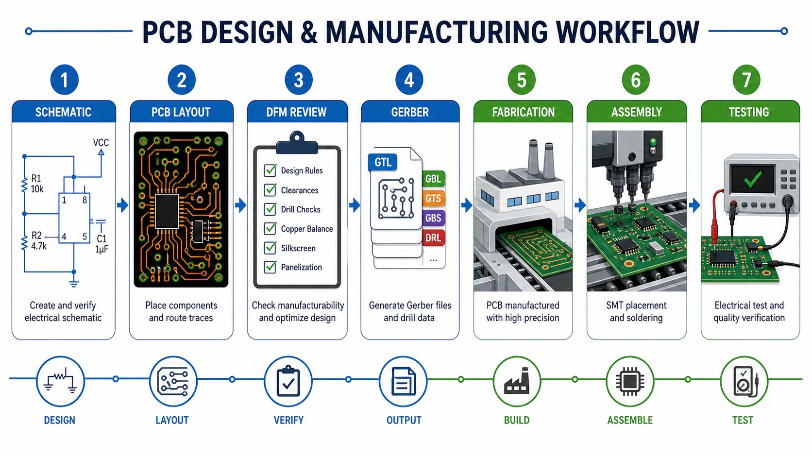
PCB design and manufacturing should be planned as one workflow, not two separate jobs. A board layout that looks complete in CAD can still fail manufacturing review if the stackup, copper, spacing, drill, solder mask, panelization, assembly access or test points are not checked before release.
For buyers and engineers, the safest path is simple: design the circuit, review the board for manufacturability, export complete files, then quote fabrication and assembly with the same technical assumptions. EBest Circuit helps customers connect DFM review, bare board production and optional PCBA so fewer problems move from design files into production.
Is your PCB design ready for manufacturing, or only ready for export?
Many projects reach RFQ stage with files that look finished but still hide production risk:
- Trace spacing, drill size or annular ring is too aggressive for the selected copper weight.
- The stackup does not match the requested material, board thickness or impedance target.
- Silkscreen, solder mask openings or component courtyards create assembly problems.
- Panelization, fiducials and test points are missing, so manufacturing and assembly teams must guess.
- The supplier quotes only the bare board while BOM, CPL and testing needs are handled too late.
EBest Circuit reviews design files through a manufacturing and assembly lens.
- We check Gerber, drill, drawing, stackup, copper, solder mask and surface finish before production release.
- We flag manufacturability risks that can affect fabrication, SMT assembly, through-hole assembly or testing.
- We support FR4, HDI, heavy copper, metal core, ceramic, flex and rigid-flex project discussions when files require more than standard review.
- We can quote bare boards and PCBA together when the project needs BOM, CPL and assembly drawing review.
PCB Design and Manufacturing in One Practical Answer
PCB design defines the circuit layout, while PCB manufacturing turns that layout into a physical board; the two must be checked together through DFM review. Good design-for-manufacturing work reduces redesign, quote changes, production delay and assembly risk.
Why Design Files Fail at Manufacturing Stage
Design files usually fail because electrical layout choices were not checked against real fabrication limits. Common examples include too-small vias, narrow solder mask bridges, copper imbalance, unclear board outline, missing drill tables and incomplete fabrication notes.
A useful RFQ package tells the manufacturer not only what the circuit is, but how it should be built, finished, inspected and assembled.
DFM Review Before PCB Manufacturing
DFM review checks whether a PCB layout can be built reliably before CAM work and production begin. It should cover stackup, material, copper, minimum trace and space, hole type, annular ring, solder mask, silkscreen, outline, panelization and test access.
For related manufacturing planning, see our PCB manufacturing and assembly guide.
Stackup, Material and Copper Decisions
Stackup, laminate and copper should be locked before the buyer compares prices. FR4 material may use low Tg, mid Tg or high Tg options, while special projects may need Rogers, PTFE, ceramic, aluminum or other materials. Copper weight affects spacing, heat rise, plating, etching and cost.
For FR4 project context, see the FR4 PCB capability page.
Layout Checks That Protect Fabrication
The most important fabrication checks are trace width, spacing, drill size, annular ring, copper-to-edge clearance and solder mask bridge. These details decide whether the board can be built as standard or needs special confirmation.
| Design Item | Manufacturing Risk | Buyer Action |
|---|---|---|
| Trace / spacing | Etching or solder bridge risk | Match rules to copper weight |
| Drill / pad | Weak plated hole or breakout | Check finished hole and annular ring |
| Board outline | Routing, V-cut or enclosure fit issue | Send mechanical drawing |
| Solder mask | Assembly yield risk | Review openings and bridges |
| Panelization | Cost and handling changes | Confirm rail, fiducial and breakaway needs |
Need a DFM check before PCB manufacturing?
Send Gerber, drill, stackup, drawing, quantity and assembly notes. EBest Circuit can review the files before quote and production release.
Gerber, Drill, Drawing and BOM Package
A complete file package reduces quote changes and manufacturing questions. For bare boards, send Gerber or ODB++, NC drill, drawing, stackup, material, copper, finish, quantity and test requirements. For assembly, add BOM, CPL, assembly drawing and approved substitutions.
PCB Fabrication Process After Design Release
After release, fabrication moves through CAM review, material preparation, imaging, drilling, plating, etching, solder mask, surface finish, profiling, inspection and electrical test. The cleaner the design package is, the fewer decisions need to be corrected during CAM.
For bare board sourcing details, see our bare PCB manufacturer RFQ guide.
Assembly Planning During PCB Design
Assembly planning should start during layout, not after bare boards arrive. Component spacing, polarity marks, fiducials, test pads, panel rails and connector orientation all affect SMT and through-hole production.
If your project needs turnkey support, EBest Circuit can review fabrication data together with BOM and CPL. See our PCBA service.
Testing and Quality Checks
Testing confirms whether the design intent survived manufacturing and assembly. Bare boards may need electrical test for opens and shorts. Assemblies may need AOI, functional testing, programming, inspection reports or project-specific test fixtures.
Cost Drivers From Design to Manufacturing
Cost is shaped by design choices before the RFQ is sent. Layer count, board size, material, copper weight, surface finish, drill count, tolerance, impedance, solder mask, test method, assembly complexity and quantity all affect the final quote.
When to Move From Two Layers to Multilayer
Move to multilayer PCB when routing density, signal return, power integrity or impedance control cannot be handled safely on one or two copper layers. Staying with too few layers can create more cost through redesign and debugging than the stackup saves.
Supplier Questions Before Sending the Order
Ask questions that reveal whether the supplier can connect design review with real production.
- Can you review DFM before formal production release?
- Which design rules change with copper weight and surface finish?
- Can you quote bare PCB and PCBA from the same file package?
- What files are missing for a reliable manufacturing quote?
- Will you flag assembly and testing risks before boards are built?
RFQ Checklist for PCB Design and Manufacturing
The RFQ should include enough information for engineering review, not only price calculation.
- Gerber or ODB++ files
- NC drill file and fabrication drawing
- Stackup, material, board thickness and copper weight
- Surface finish, solder mask and silkscreen notes
- Quantity, target schedule and testing requirements
- BOM, CPL and assembly drawing if PCBA is needed
FAQ About PCB Design and Manufacturing
These questions help buyers connect layout decisions with manufacturing results.
What is PCB design and manufacturing?
PCB design creates the circuit layout, and PCB manufacturing fabricates that design into a physical board through material preparation, drilling, plating, etching, solder mask, finish and test.
Why is DFM important before PCB manufacturing?
DFM review finds layout and file issues before production, reducing redesign, delay, quote changes and assembly risk.
Can EBest Circuit review my PCB design before quote?
Yes. Send Gerber, drill, drawing, stackup and project notes, and EBest Circuit can review the file package before preparing the manufacturing scope.
Can PCB design and assembly be reviewed together?
Yes. When PCBA is required, send BOM, CPL and assembly drawings with the PCB files so fabrication and assembly risks can be checked together.
Final Recommendation
Treat PCB design and manufacturing as one connected engineering path. The best time to control cost, schedule and quality is before files enter production, when DFM, material, copper, drill, finish, assembly and testing can still be aligned.
To review a PCB design and manufacturing project with EBest Circuit, send Gerber or ODB++, NC drill, fabrication drawing, stackup, material, copper, finish, quantity, target schedule and any BOM/CPL files to sales@bestpcbs.com. Our team will check manufacturability and prepare a practical quote scope.
You may also like





Tags: DFM Review, pcb design, pcb manufacturing