PCB manufacturing PCB manufacturing
Home > Blog

industrial pcb

Industrial PCB Manufacturing Quality Checklist for Buyers
Wednesday, July 15th, 2026
Industrial PCB manufacturing quality review and inspection

Industrial PCB manufacturing means building circuit boards for equipment where reliability, repeatability, traceability, and production readiness matter more than a simple low-cost board order. For buyers, the useful question is not only how a PCB is made. The better question is what must be checked before an industrial board is released to fabrication, assembly, inspection, and field use.

This guide is written for engineers, purchasing teams, and product teams preparing PCB builds for industrial controls, power modules, automation equipment, test instruments, LED systems, sensors, and embedded electronics. It gives a practical checklist for DFM, material choices, manufacturing files, inspection, supplier questions, and RFQ preparation.

Industrial PCB Manufacturing at a Glance

Industrial PCB manufacturing should connect design review, bare board fabrication, assembly planning, testing, and supplier communication into one controlled workflow. A board may pass a basic electrical test and still create problems if the stackup, thermal path, soldering method, component sourcing, or field environment was not reviewed early.

Area What to confirm Why it matters for industrial projects
Design files Gerber or ODB++, drill file, stackup, notes, drawing Prevents missing data, wrong layer interpretation, and quote delays.
Build requirements Layer count, copper, thickness, surface finish, impedance, material Controls manufacturability, heat, mechanical fit, and repeatability.
Assembly inputs BOM, CPL, polarity, placement notes, special soldering needs Reduces component, orientation, soldering, and rework risk.
Quality control Inspection method, test points, acceptance criteria, packaging Improves consistency before boards reach equipment integration.

When This Manufacturing Checklist Fits Your Project

This checklist fits projects where the PCB must work reliably inside industrial equipment, not only prove a circuit concept on a bench. It is useful when a failed board can stop a machine, create service cost, delay installation, or cause repeated field troubleshooting.

Use it before releasing boards for automation controllers, power conversion modules, control panels, instrumentation, industrial lighting, sensor interfaces, and other equipment that needs stable production. If your project also needs mounted components, compare the PCB build notes with the PCBA and PCB assembly service requirements before sending the RFQ.

Start With the Real Use Environment

The operating environment should guide PCB material, copper, spacing, coating, assembly, and testing decisions before the quote is finalized. Industrial boards may face heat, vibration, current load, dust, humidity, long service life, or maintenance constraints. These conditions can change the safest build approach.

Share the expected operating temperature range, enclosure type, airflow, power load, vibration exposure, connector stress, and installation environment where possible. Avoid turning these into vague notes such as “industrial grade” without explaining what the board must survive.

DFM Review Before Industrial PCB Production

DFM review checks whether the design can be manufactured consistently, inspected properly, and assembled without avoidable process risk. For industrial boards, DFM should happen before the purchase order, not after the supplier has already opened the job.

Important review points include annular ring, drill-to-copper clearance, solder mask bridges, copper balance, panelization, board outline, slot and cutout instructions, edge clearance, component-to-board edge distance, silkscreen clarity, test point access, and thermal copper behavior. The PCB design for manufacturability checklist is a useful supporting guide for the design-side review.

PCB Materials and Stackup Decisions

Material and stackup decisions should match the electrical, thermal, mechanical, and assembly needs of the industrial product. Standard FR-4 can be suitable for many projects, while high-Tg, high-frequency, metal-core, ceramic, flex, rigid-flex, or heavier copper constructions may be needed for specific operating conditions.

Do not rely on a supplier to guess the material path from the Gerber files alone. Provide target board thickness, copper weight, layer count, impedance needs, surface finish, soldering temperature exposure, and any thermal or mechanical constraints. Exact capability limits should be confirmed from the latest Best Technology process capability files before quoting, especially for special materials or non-standard structures.

Copper, Heat and Current-Carrying Requirements

Industrial PCB reliability often depends on whether the copper design, thermal path, and current load are treated as manufacturing requirements instead of late-stage troubleshooting topics. Power traces, connectors, MOSFETs, LEDs, relays, motor control sections, and high-current paths need early review.

For current-heavy or heat-sensitive designs, provide target current, expected temperature rise limits, copper weight expectations, thermal interface notes, enclosure information, and whether the board contacts a heat sink or metal chassis. This helps the supplier identify when heavier copper, wider traces, thermal vias, metal-core material, or layout changes may be needed.

Surface Finish, Solder Mask and Special Processes

Surface finish and special process choices should be selected for assembly method, shelf life, pad geometry, and product environment. The right finish for one prototype may not be the best choice for a production board with fine-pitch components, connectors, or repeated field service.

Decision Buyer question to ask Risk if ignored
Surface finish Does the finish match fine pitch parts, soldering method, shelf life, and cost target? Poor solderability, pad flatness issues, or unnecessary cost.
Solder mask Are mask dams, clearances, and openings suitable for the component pitch? Solder bridging, exposed copper, or inspection confusion.
Special processing Are slots, countersinks, impedance, peelable mask, or selective finish needs documented? Quote revisions and manufacturing holds.

Assembly Planning for Industrial PCB Builds

Assembly planning should connect BOM, CPL, placement drawings, soldering method, inspection access, and test coverage before production starts. Even when the first order is for bare boards, future assembly needs can influence panel design, fiducials, test pads, and connector placement.

For PCB assembly, prepare a clean BOM, CPL, assembly drawing, polarity notes, substitute approval rules, and packaging requirements. If the supplier is also expected to help source components, use the component sourcing service as a reference point for BOM availability, alternates, and purchasing constraints.

Inspection and Testing Requirements

Testing requirements should be defined before the order because industrial PCB quality depends on what is inspected, how defects are caught, and what acceptance criteria apply. A generic “test before shipment” request is not precise enough for many production boards.

Common checks may include visual inspection, automated optical inspection, electrical test for bare boards, X-ray for hidden solder joints when needed, dimensional checks, and customer-defined functional testing. If functional testing is required, provide the test method, fixture needs, firmware, pass/fail limits, connector access, and safety precautions.

How to Compare Industrial PCB Manufacturing Suppliers

Compare suppliers by their ability to prevent production risk, not only by the lowest unit price. A suitable supplier should ask clarifying questions, flag missing data, explain manufacturing constraints, and document quote assumptions clearly.

  • Can the supplier review Gerber or ODB++ files before production?
  • Can they explain material, finish, copper, and stackup tradeoffs?
  • Can they support both bare board fabrication and assembly when needed?
  • Can they discuss inspection and testing based on the actual board risk?
  • Do they provide clear communication when a requirement needs engineering confirmation?
  • Do they avoid unsupported promises about lead time, certification, or yield?

What Determines Industrial PCB Manufacturing Cost?

Industrial PCB cost is shaped by board complexity, material choice, copper, finish, testing, assembly requirements, quantity, and how complete the RFQ package is. A cheap first quote can become expensive when missing assumptions are corrected later.

Cost factor Why it changes price How to reduce quote uncertainty
Layer count and stackup More layers and controlled builds need more process control. Provide stackup expectations and impedance notes early.
Material and copper Special materials and heavier copper affect sourcing and processing. State material targets, copper weight, and thermal needs.
Surface finish Finish affects assembly, shelf life, pad flatness, and cost. Choose based on component pitch and product needs.
Testing More inspection or functional checks add setup and labor. Define the exact pass/fail criteria and test method.
Assembly and sourcing BOM availability and assembly method affect schedule and price. Send BOM, CPL, approved alternates, and sourcing rules.

Files to Prepare for an Industrial PCB RFQ

A complete RFQ package lets the supplier quote the real project instead of quoting a partial guess. The more industrial risk your board carries, the more important it is to include the build notes and test expectations with the design files.

  • Gerber or ODB++ fabrication data
  • Drill files and board outline drawing
  • Stackup, material, copper, finish, and thickness notes
  • Controlled impedance requirements if applicable
  • BOM, CPL, assembly drawing, and polarity notes for PCBA
  • Quantity, prototype or production stage, and target delivery window
  • Inspection, electrical test, functional test, packaging, and labeling requirements

If you prefer to prepare an online quote package first, the PCB manufacturer online guide explains how buyers can organize the same information before contacting a supplier.

Common Industrial PCB Manufacturing Risks

The most common risks are incomplete files, unclear operating conditions, weak DFM review, BOM uncertainty, unverified special processes, and vague testing requirements. These risks usually appear as quote revisions, production holds, rework, or field issues.

Do not hide uncertainty in short notes. If a requirement is not final, label it as a target and ask the supplier to confirm feasibility. If a component may change, define who approves substitutions. If a board has thermal or vibration exposure, explain the real use case instead of assuming the supplier will infer it from the layout.

Frequently Asked Questions About Industrial PCB Manufacturing

Is industrial PCB manufacturing different from standard PCB fabrication?

Yes. The fabrication steps may look similar, but industrial projects usually need more attention to operating environment, DFM, repeatability, material choices, current load, inspection, and long-term reliability.

Can one supplier handle both PCB manufacturing and assembly?

Yes, when the supplier supports both fabrication and PCBA. A combined path can reduce handoff problems because Gerber, BOM, CPL, assembly notes, and testing requirements can be reviewed together.

What should I send for an industrial PCB quote?

Send Gerber or ODB++, drill files, stackup notes, material and finish requirements, quantity, target schedule, and any testing or packaging requirements. For assembly, also send BOM, CPL, and assembly drawings.

Should I choose the cheapest industrial PCB supplier?

Not automatically. Low price is useful only when the quote includes the real material, process, inspection, assembly, and testing requirements. Compare assumptions before comparing unit price.

Final RFQ Recommendation

Before placing an industrial PCB manufacturing order, prepare the files and risk notes that let the supplier review the project as a real production build. A strong RFQ package should include Gerber or ODB++, drill data, stackup, material, copper, finish, BOM, CPL, drawings, quantity, testing requirements, packaging notes, and target delivery timing.

For an engineering review or quotation, send your Gerber or ODB++ files, BOM, CPL, mechanical drawings, quantity, material expectations, surface finish, test requirements, and target lead time to sales@bestpcbs.com. The Best Technology / bestpcbs team can review the manufacturing path, confirm what needs project-specific checking, and help you prepare the next industrial PCB build without relying on hidden assumptions.

You may also like

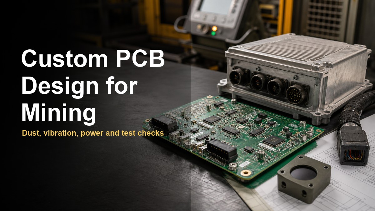
Custom PCB Design for Mining: Dust, Vibration and Power Checks
Monday, July 13th, 2026
Custom PCB design for mining equipment with rugged enclosure and connector harness

Custom PCB design for mining equipment should be reviewed around dust, moisture, vibration, protected power input, connector strain relief, thermal control, test points and production-ready RFQ files. A mining electronics board is not only a circuit layout. It is part of a rugged system that may sit near motors, pumps, sensors, conveyors, vehicles, lighting, chargers or communication devices where contamination, shock and repair access matter.

This guide is written for engineers and buyers preparing a custom PCB or PCBA for mining-related equipment. It focuses on practical design and manufacturing checks before fabrication or assembly. If the product will be used underground, near combustible dust, or in another regulated hazardous area, confirm the applicable equipment-level certification requirements with your compliance team. A PCB supplier can support design for reliability, traceability and production quality, but board fabrication alone does not certify the complete mining device.

What does custom PCB design for mining need to solve?

Mining PCB design needs to keep electrical performance stable while the board is exposed to dust, vibration, heat, moisture, long cable runs and maintenance stress. The exact risks depend on whether the board is used in a sensor node, motor controller, lighting module, communication gateway, battery system, display panel or test device.

For a simple monitoring module, the main issues may be enclosure fit, connector sealing and low-power reliability. For a power or drive-related board, the review moves toward copper weight, creepage and clearance, thermal paths and protection components. Compact control electronics may also need an HDI PCB if the enclosure is tight and the component density is high.

Mining design risk PCB or PCBA check Why it matters
Dust and moisture Enclosure interface, coating decision, connector sealing and cleaning process Contamination can create leakage paths, corrosion and intermittent faults
Vibration and shock Mounting holes, board support, connector retention and heavy component placement Loose connectors or cracked solder joints can stop equipment in the field
Power variation Input protection, grounding, copper width, fusing and transient protection Long cables and inductive loads can create voltage stress
Heat buildup Copper weight, thermal vias, enclosure contact and material selection Sealed boxes often have limited airflow
Maintenance Test points, labels in drawings, harness plan and replaceable modules Field teams need faults isolated quickly without damaging the board

Where are custom mining PCBs used?

Custom mining PCBs are common in control, sensing, communication, lighting, power conversion and equipment monitoring devices. A buyer should define the use case before asking for a quote, because a sensor interface board and a high-current control board need different materials, copper rules and test plans.

Typical examples include conveyor monitoring electronics, pump controllers, battery management devices, rugged displays, LED lighting modules, wireless gateways, environmental sensors and vehicle-mounted control units. Some designs use standard FR4 PCB construction. Others need heavier copper, higher Tg material, metal-backed structures, conformal coating, sealed box integration or full PCBA support.

How should dust, moisture and enclosure fit be handled?

The PCB should be designed together with the enclosure, gasket, connector system and cleaning/coating plan. Treating the board as a flat electrical drawing and the enclosure as a later mechanical decision often creates failures at cable entries, mounting bosses, edge clearance and service access.

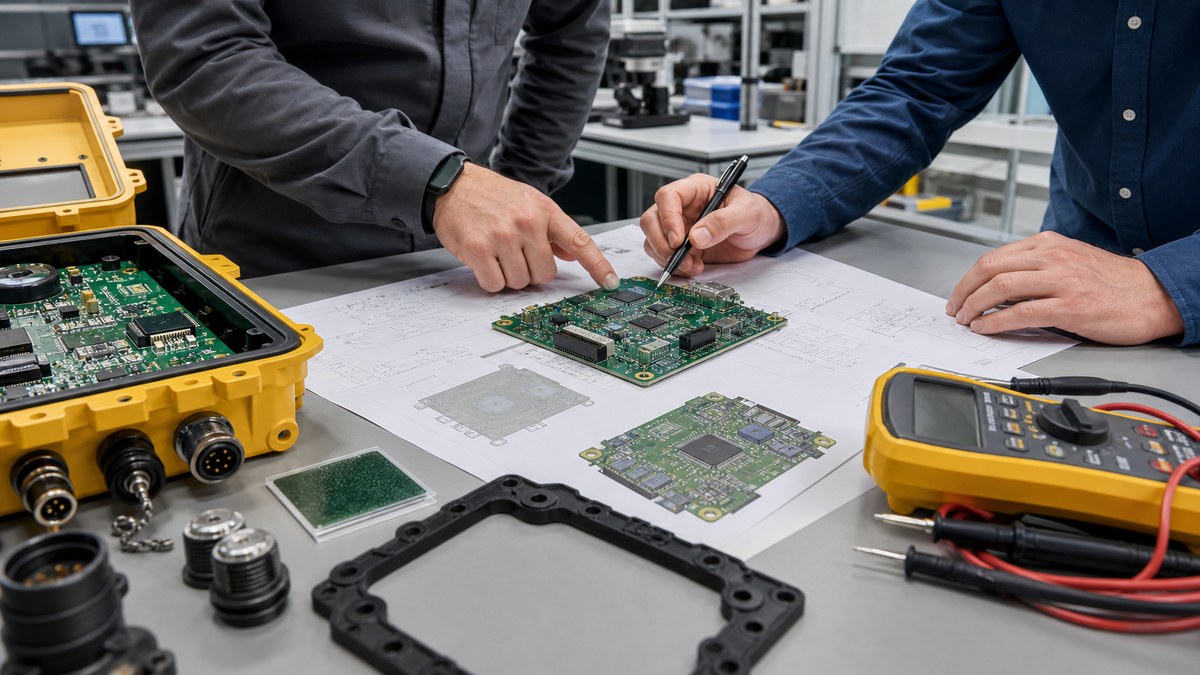
Engineers reviewing a rugged mining equipment PCB with enclosure gasket and connector samples
Mining electronics should be reviewed as a board, enclosure, connector and testable assembly, not as a bare PCB only.

Before layout release, check the board outline against the enclosure drawing, connector keepout area, mounting-hole tolerance, coating keepout, service connector position and any pressure-equalization or sealing requirement. If conformal coating is planned, mark no-coat areas around connectors, switches, programming pads and test contacts. If potting is planned, confirm component height, thermal behavior and repair expectations before the production file is frozen.

What vibration checks matter before production?

Vibration risk is controlled by board support, connector retention, solder joint protection and heavy component placement. A mining PCB can pass an electrical review and still fail in the field if a large inductor, terminal block, relay, transformer, battery connector or harness load is not mechanically supported.

Use larger mounting margins around high-stress areas. Keep heavy parts away from unsupported board edges when possible. Add strain relief for harnesses instead of letting cable pull act directly on solder joints. For mixed SMT and through-hole designs, define whether wave soldering, selective soldering or hand operations are expected. If the design includes high-current terminals, compare the copper and spacing assumptions against a relevant design reference such as the Heavy Copper PCB Design Guide.

How should power input and heat be reviewed?

Power input review should cover voltage range, surge exposure, reverse polarity risk, grounding, heat flow and copper current capacity. Mining equipment often connects through long cables, battery systems, motors, relays, lighting modules or chargers. These conditions can put more stress on input circuits than a clean lab supply.

For early DFM, send the supplier the expected operating voltage, maximum current, copper weight, target temperature range, board thickness, surface finish and any thermal interface to the enclosure. Do not ask for only a bare board price if the real product needs heat-spreading, coated assembly, heavy connectors or functional testing. The quote should reflect the way the board will be used.

Design area Questions to answer before RFQ
Input power What voltage range, current load, fuse strategy and reverse-polarity protection are required?
Grounding How are chassis ground, signal ground and shield termination handled?
Thermal path Will heat leave through copper pours, vias, thermal pads, an enclosure wall or a heatsink?
Copper weight Are high-current traces sized for the real load and temperature rise target?
Protection Are surge, ESD and inductive switching risks reviewed at cable and connector interfaces?

Which materials and stackups fit mining electronics?

The material choice should follow the electrical load, enclosure temperature, vibration risk and required board density. FR4 is often suitable for control and sensor boards, but high-current, high-heat or compact assemblies may need different copper, laminate, via and thermal decisions.

For dense signal boards, HDI can reduce routing congestion and help fit a smaller rugged enclosure. For power boards, thicker copper, larger spacing and thermal planning may matter more than density. For LED lighting or heat-generating modules, metal-backed or direct thermal path designs may be considered. The right choice depends on the project files, not on a generic mining label.

How should assembly and sourcing be planned?

Mining PCBA planning should include component availability, substitute approval, coating or sealing steps, test fixture needs and final box-level handling. A bare PCB schedule does not describe the finished product if the order also needs SMT, through-hole assembly, wiring, enclosure fit or functional testing.

Before releasing the order, provide a controlled BOM, approved alternates, centroid file, assembly drawing, polarity notes, connector orientation, firmware loading requirement and test criteria. If long-life parts or industrial-grade components are required, discuss Component Sourcing early. If the supplier is expected to deliver a mounted board in a sealed housing, treat it as a Box Build Assembly discussion rather than a normal PCB-only purchase.

What test plan should be ready before release?

The test plan should prove the board can be built, inspected and checked consistently before it reaches the field. At minimum, define electrical test for bare boards, AOI or visual inspection for assembly, functional checks for powered boards and any project-specific connector, LED, sensor, relay or communication test.

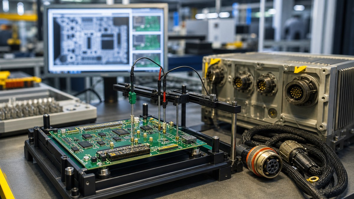
Mining equipment PCB assembly under electrical test with rugged connector harness and sealed enclosure
Testing should be planned before production release, especially when cables, connectors, sealed boxes and field power inputs are involved.

Useful test points should be accessible after assembly, not hidden under large components or blocked by the enclosure. If the board has firmware, define how programming and verification are handled. If the product uses sensors, motors, relays or communication interfaces, list the pass/fail behavior in simple language. A supplier’s PCB test equipment capability should be part of the RFQ discussion when the board needs repeatable inspection instead of only continuity checks.

RFQ checklist for custom PCB design for mining

A useful RFQ package lets the supplier review reliability risks before quoting cost and lead time. Send the same controlled package to every supplier if you want to compare quotes fairly.

  1. Gerber files, drill files, netlist and controlled revision number.
  2. Board drawing with thickness, outline tolerance, mounting holes and connector keepouts.
  3. Stackup, copper weight, material preference and surface finish requirement.
  4. Expected operating voltage, current load, thermal concern and enclosure notes.
  5. BOM, approved substitutes, centroid file and assembly drawing if PCBA is included.
  6. Coating, potting, cleaning, labeling, packaging or box-build requirements.
  7. Test plan with required measurements, programming steps and pass/fail criteria.
  8. Compliance notes for the final equipment, especially if the use environment is regulated.

Supplier questions buyers should ask

The best supplier questions are specific enough to reveal whether the factory has reviewed the board as a mining electronics assembly, not just a generic PCB. Use the questions below before approving production.

  • Which part of this design creates the highest manufacturing risk?
  • Are the mounting holes, edge clearances and connector keepouts suitable for the enclosure?
  • Is the copper weight enough for the stated current and temperature target?
  • Do any components need adhesive, mechanical support or layout changes for vibration?
  • Which components have sourcing risk, and are substitutes already approved?
  • Can the test points still be reached after assembly or box build?
  • What should be changed before moving from prototype to production?

FAQ

What is custom PCB design for mining?

Custom PCB design for mining means designing a circuit board or PCBA for equipment used around mining operations, such as sensors, controllers, lighting, communication modules, power electronics or monitoring devices. The design must consider dust, vibration, moisture, power stress, enclosure fit, connectors, testing and production repeatability.

Does a mining PCB need a special material?

Not always. Many mining control or sensor boards can use FR4 when the electrical load and temperature are moderate. High-current, high-heat, compact or harsh-environment designs may need heavier copper, higher-grade laminate, HDI, metal-backed construction, coating or a different stackup. The material should follow the real design risk.

Can a PCB supplier certify mining equipment?

A PCB supplier can support reliable board fabrication, assembly, traceability, inspection and documentation. Certification for equipment used in regulated mining or hazardous environments is usually a system-level issue. Confirm ATEX, IECEx, MSHA or local requirements with qualified compliance specialists before production decisions.

What files are needed for a mining PCB quote?

Send Gerber files, drill files, board drawing, stackup, copper weight, surface finish, BOM, centroid file, assembly drawing, enclosure notes and test requirements. If the board will be coated, potted or installed in a sealed box, include those details in the first RFQ instead of adding them later.

What causes delays in mining PCB projects?

Common delays include unclear enclosure drawings, missing connector orientation, unapproved component substitutes, vague test criteria, incomplete power requirements and late coating or box-build decisions. A controlled RFQ package helps the supplier check manufacturability before committing to lead time.

Conclusion

Custom PCB design for mining should be treated as a rugged electronics project, not a normal board order with a different label. Start with the environment, enclosure, connectors, power input, heat path, component sourcing and test plan. Then ask the supplier to review the files for manufacturability before quote approval. That process gives the buyer a better chance of receiving a board that can be assembled, inspected and supported in real mining equipment.

You may also like

Custom PCB Design for Industrial Use: Enclosure, Power and I/O Checks
Monday, July 13th, 2026
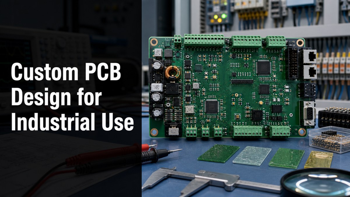
Custom PCB design for industrial use with terminal blocks, power circuitry and test tools

Custom PCB design for industrial use means designing the bare board and assembly around the real installation: enclosure size, field wiring, power noise, vibration, temperature, moisture, service access and test coverage. A board that works on a lab bench can still fail in a cabinet, pump controller, sensor node or factory gateway if the PCB layout ignores connectors, grounding, protection, mounting and production test points.

For an industrial product, the best PCB design brief is not only a schematic and a Gerber file. It should explain the operating voltage range, load current, connector map, enclosure limits, ambient temperature, coating or potting needs, expected service life, and how the board will be tested before shipment. Those details help the PCB manufacturer catch risk before the design moves into fabrication and assembly.

What Is Custom PCB Design for Industrial Use?

Custom PCB design for industrial use is the process of turning an industrial product requirement into a manufacturable board layout that can survive field wiring, power variation, mechanical stress and repeatable production testing. It is different from a generic electronics board because the installation environment becomes part of the design input.

An industrial controller, power monitor or equipment interface often needs larger terminal blocks, screw mounting holes, isolation gaps, surge protection, clear service labels and room for hand tools. The base material may still be a standard FR4 Printed Circuit Board, but the layout rules, copper weight, coating decision and connector placement should be chosen for the real equipment, not for a clean prototype demo.

Start With the Enclosure, Not Only the Circuit

The enclosure fixes many PCB design decisions before trace routing begins. Board outline, mounting holes, connector direction, LED visibility, cable bend radius, airflow and service clearance all depend on the box or cabinet where the board will be installed.

Before layout, confirm the board outline against the mechanical drawing. Check whether connectors must face a panel opening, whether screw terminals need finger access, and whether high-voltage or high-current areas need physical separation from signal wiring. If the board is part of a complete product rather than a loose PCB, coordinate early with the Box Build Assembly plan so cable routing, labels, displays and mechanical fasteners are not solved after the PCB is already finished.

Enclosure factor PCB design check Why it matters
Mounting points Hole size, copper keep-out, washer clearance Prevents cracked solder joints and board flex
Panel connectors Connector height, orientation and access Avoids cable strain and rework during assembly
Airflow Heat source placement and component height Reduces hot spots in sealed or crowded cabinets
Coating or potting Keep-out around connectors, switches and test pads Prevents coating from blocking service points
Service access Readable silkscreen and reachable fuses/test points Helps technicians diagnose the unit in the field

Design the Power Input for Real Factory Conditions

Industrial PCB power design should assume voltage variation, switching noise, inrush current and wiring mistakes instead of assuming a perfect bench supply. The exact protection scheme depends on the product, but the layout should reserve room for protection, filtering and thermal relief.

For DC industrial boards, check reverse-polarity protection, fuse or resettable protection, surge or transient suppression, input filtering, regulator heat, copper width and connector current rating. For boards that switch motors, relays, heaters or solenoids, keep noisy current loops compact and separated from sensors, analog inputs and communication traces. High-current or high-heat industrial applications may need heavier copper, metal-core materials, ceramic substrates or another special PCB structure instead of a basic two-layer FR4 board.

Protect I/O Before It Reaches the MCU

Field I/O is one of the most common weak points in industrial PCB design because long cables carry noise, ESD, surge and wiring errors directly to the board edge. Treat every external connector as a risk entry point.

Place ESD or surge protection close to the connector when required. Keep isolation slots, creepage and clearance appropriate for the voltage category. Put pull-ups, filtering, common-mode chokes or termination near the interface they protect. For RS-485, CAN, Ethernet, sensor inputs or dry-contact I/O, make grounding and shield termination choices early so the PCB layout does not fight the installation wiring later.

Connector selection also affects assembly and sourcing. A design that depends on a rare terminal block or long-lead-time relay may be difficult to build during a shortage. Early Component Sourcing review helps confirm package availability, approved alternates and whether the BOM can support prototype and production builds.

Plan DFM, Assembly and Test Points Together

A good industrial PCB layout is not finished until assembly access and test coverage are planned. If test pads, programming headers and fixture access are added at the end, the board may pass a prototype build but become slow or expensive in production.

Confirm component orientation, panelization, fiducials, solder mask clearance, through-hole access, connector height and coating keep-outs before release. For the assembled product, define which rails, interfaces and functional outputs must be checked. The layout should include accessible test pads for ground, input voltage, main regulators, communication signals and critical sensor lines. A related engineering guide on Circuit Board Test Points can help teams decide which signals deserve fixture access before the first production batch.

If the supplier will handle both PCB fabrication and PCBA, PCB Assembly, SMT, PCB SMT by EBest Circuit (Best Technology), send the assembly drawing, BOM, pick-and-place file, test plan and coating requirements together. Separating fabrication questions from assembly questions often hides problems until parts are already on order.

Industrial PCB Design Checklist Before RFQ

The RFQ package should let the manufacturer review risk, not just quote a board size and layer count. Missing details usually turn into delayed questions, wrong assumptions or rework.

  • Gerber files, drill files, stackup notes and controlled impedance needs if applicable.
  • Board outline with enclosure drawing or DXF when connectors and mounting holes are critical.
  • BOM with manufacturer part numbers, approved alternates and lifecycle notes.
  • Assembly drawing with polarity marks, connector orientation and no-fit parts.
  • Expected environment: temperature, humidity, vibration, dust, splash, coating or potting.
  • Power input range, load current, surge concerns and isolation requirements.
  • Test requirements: programming, in-circuit checks, functional test and inspection points.
  • Packaging and box-build notes if the PCB ships as a complete module.

Common Mistakes That Make Industrial Boards Hard to Build

Most industrial PCB mistakes are not exotic layout errors; they are practical mismatches between the board, the cabinet, the wiring and the production process. Catching them before fabrication saves more time than debugging them after assembly.

Mistake Likely result Better design action
Connectors placed without cable clearance Field wiring bends sharply or blocks the cover Check cable path against enclosure CAD
No test access for power rails Production test becomes slow and manual Add test pads near regulators and protected I/O
Small copper paths for load current Heating, voltage drop or early failure Check copper width, copper weight and thermal relief
Protection parts far from connectors ESD or surge reaches sensitive ICs first Place protection near external entry points
No alternates for industrial connectors Build delay during component shortage Review BOM availability before final layout

Supplier Questions for an Industrial PCB Project

Use supplier questions to check whether the PCB manufacturer understands the product conditions, not only the drawing package. The answers should expose DFM gaps early.

  • Can you review connector clearance against the enclosure drawing?
  • Do any parts in the BOM have long lead time, EOL risk or weak alternates?
  • Which test points are needed for production fixture testing?
  • Should the board use thicker copper, different laminate, coating or selective keep-outs?
  • Can fabrication, assembly, coating and box build be reviewed as one workflow?
  • Which inspection records or test reports will be provided with the finished boards?

FAQ

What files are needed for a custom PCB design for industrial use?

Send Gerber and drill files, BOM, pick-and-place file, assembly drawing, board outline, enclosure drawing if available, test requirements and operating environment notes. For industrial boards, the enclosure, connector map, power range and coating requirements are often as important as the PCB data itself.

Does every industrial PCB need conformal coating?

No. Coating depends on moisture, dust, chemical exposure, voltage spacing and service requirements. If coating is needed, the PCB should include keep-outs around connectors, switches, jumpers, labels and test pads so coating does not block assembly or maintenance.

How should I choose materials for an industrial PCB?

Start with temperature, current, voltage, mechanical load and heat dissipation. FR4 is common for many control boards, but high-current, high-temperature, RF, heavy copper, metal-core or ceramic requirements may call for a different stackup or special PCB process.

Why do industrial PCBs need more test points than simple prototypes?

Production builds need repeatable checks. Test points give fixtures access to voltage rails, programming pins, communication lines and critical I/O. Without them, technicians may rely on slow manual probing or miss faults that only appear after installation.

Final Recommendation

For custom PCB design for industrial use, review the board as part of a field product: enclosure, wiring, power, I/O protection, assembly, sourcing and test coverage. The strongest RFQ package gives the manufacturer enough context to find DFM, BOM and reliability risks before the first boards are built.

You may also like

Custom PCB Design for Industrial Networks
Saturday, July 11th, 2026
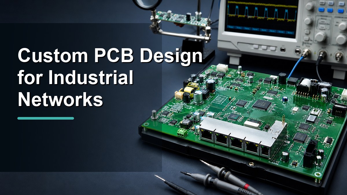
Custom PCB design for industrial networks with Ethernet connectors on an engineering test bench
Industrial network PCB design should be reviewed around signal integrity, power, EMC, connector reliability, and production files before release.

Custom PCB design for industrial networks means building a printed circuit board for reliable data communication in machines, controllers, gateways, sensors, and field devices. The board must handle Ethernet or other network signals, stable power, EMC risk, connector stress, surge exposure, thermal load, and production repeatability at the same time.

For buyers and hardware engineers, the practical question is not only whether the circuit works on the bench. The real question is whether the PCB can be fabricated, assembled, tested, and used in a noisy industrial environment without repeated layout changes. That is why this article focuses on design checks, manufacturing files, and supplier review points for industrial network PCB projects.

What Is Custom PCB Design for Industrial Networks?

Custom PCB design for industrial networks is the process of creating a circuit board layout for devices that exchange data in factory, automation, monitoring, or machine-control environments.

These boards may support industrial Ethernet, RS-485, CAN, PoE, wireless modules, sensor interfaces, edge controllers, gateways, or mixed-signal control circuits. Unlike a generic development board, a custom industrial network PCB must fit the product enclosure, connector position, cable strain, operating temperature, power budget, and final assembly process.

The design work usually starts from schematic and layout, but it should not end there. The PCB also needs stackup definition, impedance planning, connector footprint control, ESD and surge protection, test access, and a manufacturable release package. For projects that need custom board types, review the available custom PCB and PCBA solutions early instead of waiting until the layout is already locked.

Where Industrial Network PCBs Are Used

Industrial network PCBs are used wherever electronic equipment must communicate reliably with other devices under electrical noise, vibration, temperature variation, or long cable runs.

Application Typical board requirement Main design risk
PLC and I/O modules Ethernet, RS-485, isolated inputs, dense connectors Noise coupling, connector spacing, test access
Industrial gateways Multiple RJ45 ports, MCU or MPU, power regulation Impedance control, heat, ESD path
Smart sensors Sensor front end, wireless or wired data link, compact shape Analog noise, grounding, enclosure fit
PoE devices Ethernet data and power on the same cable Power loss, isolation, surge protection
Machine vision or control boards High-speed data, stable power rails, edge connectors Signal integrity, thermal rise, BOM stability

These applications often combine digital communication, power conversion, and field wiring on one board. That combination is useful, but it also creates design conflicts. The layout must keep noisy switching loops away from magnetics and data traces, give connectors enough mechanical support, and leave enough room for inspection and rework.

Key Design Checks Before Layout Release

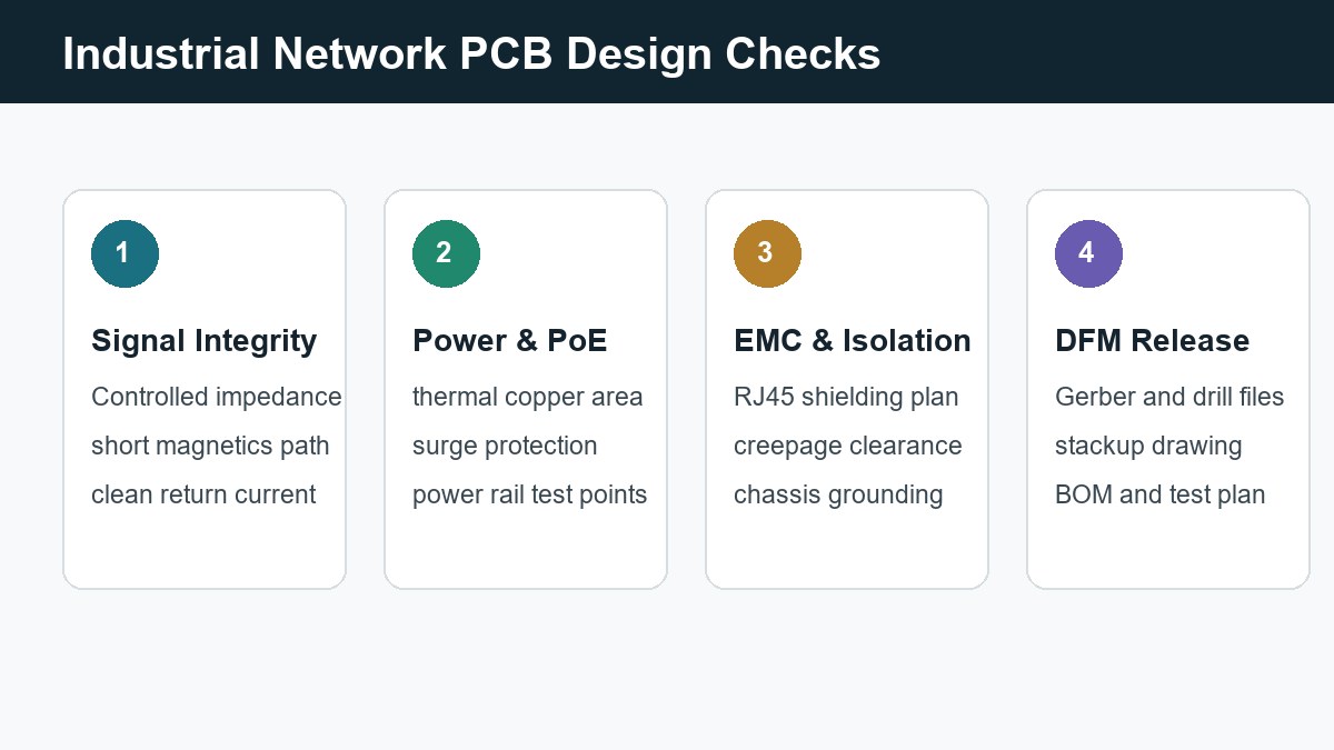
The most useful pre-release checks are signal integrity, PoE or power design, EMC and isolation, connector reliability, and DFM file readiness.

Industrial network PCB design checks for signal integrity, PoE, EMC isolation, and DFM release
Keep the design review focused on the checks that change manufacturing yield, field reliability, and debug time.

Start with the communication path. Ethernet differential pairs, high-speed sensor buses, and clock lines need controlled routing, short return paths, and careful spacing from switching power sections. If the product uses dense connectors or fast edge rates, a standard board may not be enough. In those cases, HDI PCB or tighter multilayer routing may be part of the design discussion.

Next, review power and thermal behavior. PoE, DC input modules, relays, and motor-control interfaces can push current through small board areas. Trace width, copper weight, thermal vias, fuse position, TVS diode placement, and connector current rating should be checked together. A layout that passes electrical simulation can still fail in production if heat concentrates under one regulator or if field wiring injects surge current into the wrong ground path.

Finally, check how the board will be assembled and inspected. An industrial network PCB often has RJ45 connectors, shield cans, terminal blocks, optocouplers, magnetics, LEDs, and test points. Footprint polarity, component height, solder access, and panelization should be reviewed before prototype order. If the project includes mounted components, plan the PCB assembly support at the same time as bare board fabrication.

How Stackup and Materials Affect Network Reliability

Stackup and material choice affect impedance stability, EMI behavior, thermal movement, and long-term reliability more than many buyers expect.

For many industrial control boards, FR4 is still the correct starting point. The decision is not simply “FR4 or special material.” Engineers should define board thickness, copper weight, layer count, reference planes, dielectric spacing, and operating temperature before asking for a quote. A controlled stackup helps keep Ethernet pairs consistent, gives return current a clean path, and reduces layout guesswork.

When the product must handle higher heat, tighter size, high-density connectors, or higher data rates, the board may need high Tg FR4, multilayer construction, impedance control, heavy copper, or special process review. You can use a standard FR4 printed circuit board for many designs, but do not treat the laminate as a default afterthought. Material choice should follow the electrical, thermal, and mechanical load of the device.

EMC, ESD, and Isolation Checks

Industrial network PCB design should give noise and surge current a controlled path instead of letting it travel through sensitive logic or sensor circuits.

Ethernet, RS-485, CAN, and external sensor ports usually connect to cables that may run near motors, relays, power wiring, or long metal frames. That means the PCB must consider ESD, surge, common-mode noise, shielding, creepage distance, and grounding strategy. Protection components should sit near the connector, not deep inside the board after a long trace path.

For RJ45 Ethernet, the magnetics area, shield connection, chassis reference, and differential routing deserve a dedicated layout review. For isolated inputs or fieldbus connectors, isolation slots and clearance rules must be visible in the fabrication data. For noisy power sections, keep switching loops compact and do not route sensitive communication traces under them unless the stackup and return path are deliberate.

Connector and Mechanical Reliability

Connector reliability is a PCB design issue because the board must survive cable insertion, pull force, enclosure fit, and repeated maintenance.

Industrial network products often fail at practical mechanical points: cracked solder joints under heavy connectors, weak cable strain relief, poor board support near terminal blocks, or connector openings that do not line up with the enclosure. A custom PCB should place mounting holes, keepouts, stiff areas, and connector orientation before the layout becomes crowded.

If the board needs edge connectors, shielded RJ45 jacks, terminal blocks, or unusual cutouts, include mechanical drawings with the quote package. Special board shapes, gold fingers, impedance lines, and nonstandard copper requirements should be reviewed as special PCB items rather than handled as ordinary low-risk details.

Production File Checklist for an Accurate Quote

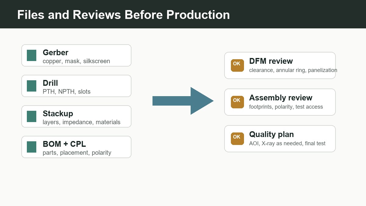
An accurate quote needs fabrication, assembly, mechanical, and testing information, not only a Gerber file.

Files and reviews before production for custom industrial network PCB projects
A complete release package reduces quote assumptions and avoids avoidable engineering questions before production.

For bare PCB fabrication, send Gerber or ODB++ files, NC drill files, board outline, stackup request, copper thickness, surface finish, solder mask color, impedance requirements, special notes, and quantity. For assembly, add the BOM, pick-and-place file, assembly drawing, polarity notes, approved alternates, programming needs, and test requirements.

Do not hide special requirements inside email text only. Put them in the drawing or release note so CAM, procurement, assembly, and quality teams see the same information. If the project is still at prototype stage, prototype PCB assembly can help validate footprints, connector fit, and test points before scaling to a larger build.

Supplier Questions Buyers Should Ask

A supplier for industrial network PCB work should be able to discuss DFM, stackup, assembly, testing, and component risk before production starts.

  • Can you review the Ethernet or high-speed routing stackup before fabrication?
  • Can you confirm minimum annular ring, drill-to-copper clearance, and slot capability?
  • Can you assemble shielded connectors, magnetics, terminal blocks, and mixed SMT/THT parts?
  • How will polarity, connector orientation, and functional test access be checked?
  • Which components in the BOM need alternates or sourcing confirmation?
  • Can you separate bare PCB, assembly, and testing cost drivers in the quote?

BOM risk is often underestimated in custom industrial electronics. Ethernet magnetics, isolated power modules, TVS arrays, terminal blocks, and industrial connectors can have long lead times or multiple acceptable alternates. For that reason, component sourcing should be reviewed before the layout is frozen, especially when footprint-compatible alternates are possible.

Common Mistakes That Delay Industrial Network PCB Projects

Most delays come from unclear files, missing mechanical details, weak test planning, and design choices that are hard to build consistently.

A common mistake is sending only Gerbers when the project also needs controlled impedance, assembly, programming, and functional testing. Another is placing Ethernet connectors and surge protection after the rest of the board is already dense. That often leads to long protection paths, poor grounding, and last-minute compromises around the enclosure.

Buyers also sometimes compare quotes without checking assumptions. One supplier may quote bare boards only, while another includes assembly, component procurement, testing, and fixture work. A lower number is not useful if it excludes the work needed to make the product shippable.

FAQ About Custom PCB Design for Industrial Networks

What makes an industrial network PCB different from a normal PCB?

An industrial network PCB usually connects to cables, machines, sensors, or controllers in electrically noisy environments. It needs stronger attention to EMC, ESD, grounding, connector strength, power stability, test access, and production repeatability than a simple low-speed control board.

Do industrial Ethernet PCBs always need controlled impedance?

Not always, but Ethernet differential pairs and faster interfaces should be reviewed for impedance, stackup, routing length, pair spacing, and return path. If cable length, data rate, EMI risk, or product reliability matters, controlled impedance planning is safer than treating the traces as ordinary signal routes.

What files should I send for a custom industrial network PCB quote?

Send Gerber or ODB++ files, drill files, board outline, stackup, material and copper requirements, BOM, pick-and-place file, assembly drawing, impedance notes, testing requirements, and any enclosure or connector constraints. More complete files reduce quote assumptions.
Can one supplier handle both PCB fabrication and assembly?

Yes, but confirm the supplier can handle the specific connector types, mixed SMT and through-hole parts, BOM sourcing, inspection, and functional test requirements. A one-stop supplier is useful only when the assembly and quality plan match the product risk.

When should component sourcing be reviewed?

Review sourcing before the layout is frozen. Industrial connectors, Ethernet magnetics, isolated modules, TVS arrays, and power components may need footprint-compatible alternates. Early review prevents redesign when a preferred part is unavailable or has an unsuitable lead time.

How can I reduce redesign risk before mass production?

Build a prototype with the real connectors, enclosure constraints, power input, and test method. Check signal behavior, heat, connector fit, assembly yield, and functional test coverage before increasing quantity. Do not rely only on schematic correctness.

Final Checks Before Sending Your Files

Before sending files for quotation or production, check whether the board has a defined stackup, clear connector placement, protected external interfaces, test points, assembly notes, and a realistic BOM.

Custom PCB design for industrial networks works best when electrical, mechanical, assembly, and sourcing requirements are reviewed together. If you are preparing an industrial Ethernet, PoE, sensor gateway, PLC module, or machine-control PCB, send your Gerber files, BOM, stackup request, connector requirements, quantity, and testing needs to sales@bestpcbs.com for engineering review and a practical quote.

You may also like

High Speed PCB Design, Industrial PCB Case Sharing
Tuesday, June 25th, 2024

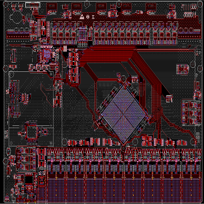
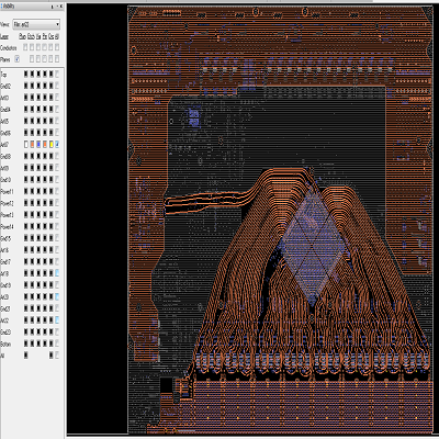
A high-speed circuit handles signals that switch quickly or operate at high frequencies, typically above 50 MHz, though some advanced systems may go into the GHz range. EBest Circuit (Best Technology) is a one-stop PCB manufacturer that covers pcb design, pcb layout, pcb diagram, DFM, SI, PI analysis, PCB manufacturing and so on. In the following, you can see a high speed pcb design solution for industrial switch that we cooperated with our customer.

32 x 400GE industrial switch

[1]: Marvell-400G chip

[2]: 200A maximum current

[3]: Single pair differential line 56G optical network

[4]: 24 layers high power PCB

What’s the Best Material for High-Speed PCB Design?

Choosing the right material is vital for maintaining signal integrity and achieving optimal performance. The material impacts the board’s dielectric constant (Dk), loss tangent, and overall signal quality. Common materials include:

  • FR4: Widely used but not ideal for very high frequencies due to higher loss tangent.
  • Rogers (RO4000 series): Preferred for high-speed designs thanks to its low dielectric constant and loss tangent.
  • Teflon: Excellent for high-frequency applications but more expensive and harder to process.

Selecting the appropriate material ensures the PCB can handle high-speed signals without compromising performance.

For the PCB design service, we can make sure the one-time success to save much time and money for customers. Our goal is to work with customers together and win more market with our clients. Just feel free to contact our technical team if you have similiar designs.
You may also like