EBest Circuit (Best Technology) Co.,Ltd
- +86-755-2909-1601
- sales@bestpcbs.com
|
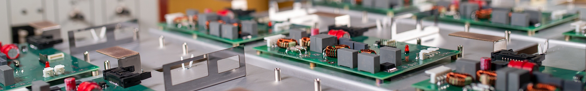
It also has same two layers of copper conductor like Double layers MCPCB, but the metal core is in the middle of two conductor, so there're conductors (trace) on both sides of metal core, and were connected to each other by Vias. So we named it "Double sided MCPCB", and you can populated SMD on both top and bottom. Different with Single layer MCPCB, double sided MCPCB also requires an additional pressing step to laminate the imaged thermal conductive laminate and metal core (also known as metal base) together. But sometimes, some raw Metal Clad material vendor will supply board material which already laminated. Compared with normal FR4, this sturcture need more technology and experience on laminating of two layers together with metal core. |
Structure of Double Sided MCPCB |
 |
| Capability of Double Sided MCPCB |
|
| Please click here for immediate quotation online Please contact us for more information about the double layers MCPCB. |
ISimply drop your email or phone number in the contact form, and we'll promptly provide you with a quotation.