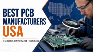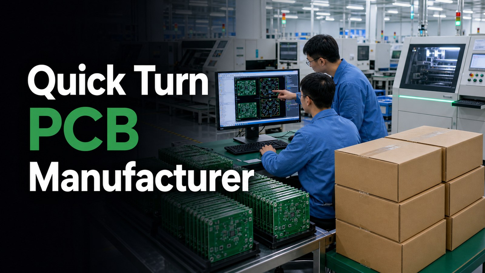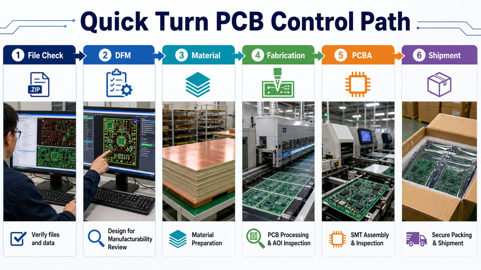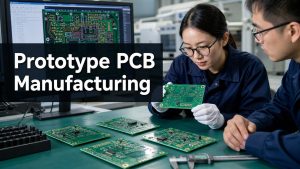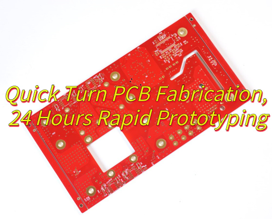
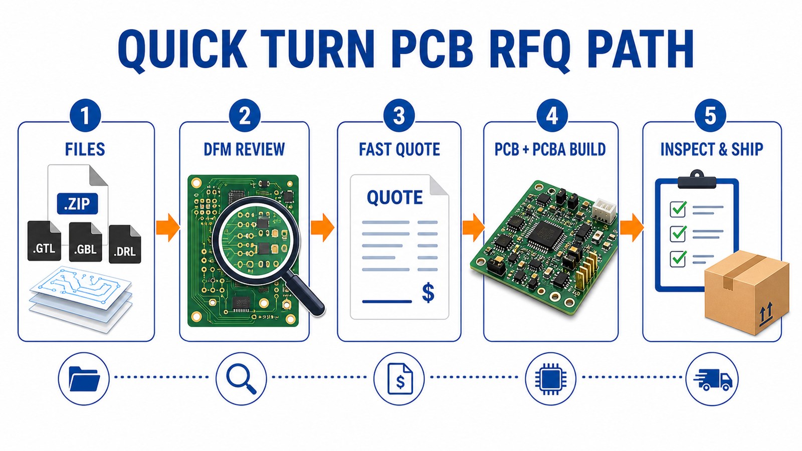
A quick turn PCB manufacturer in the USA should be compared by what it can review before the clock starts, not only by the fastest number on the quote page. Speed only helps when fabrication files, BOM/CPL, PCBA scope, inspection, testing and shipping assumptions are clear before production begins.
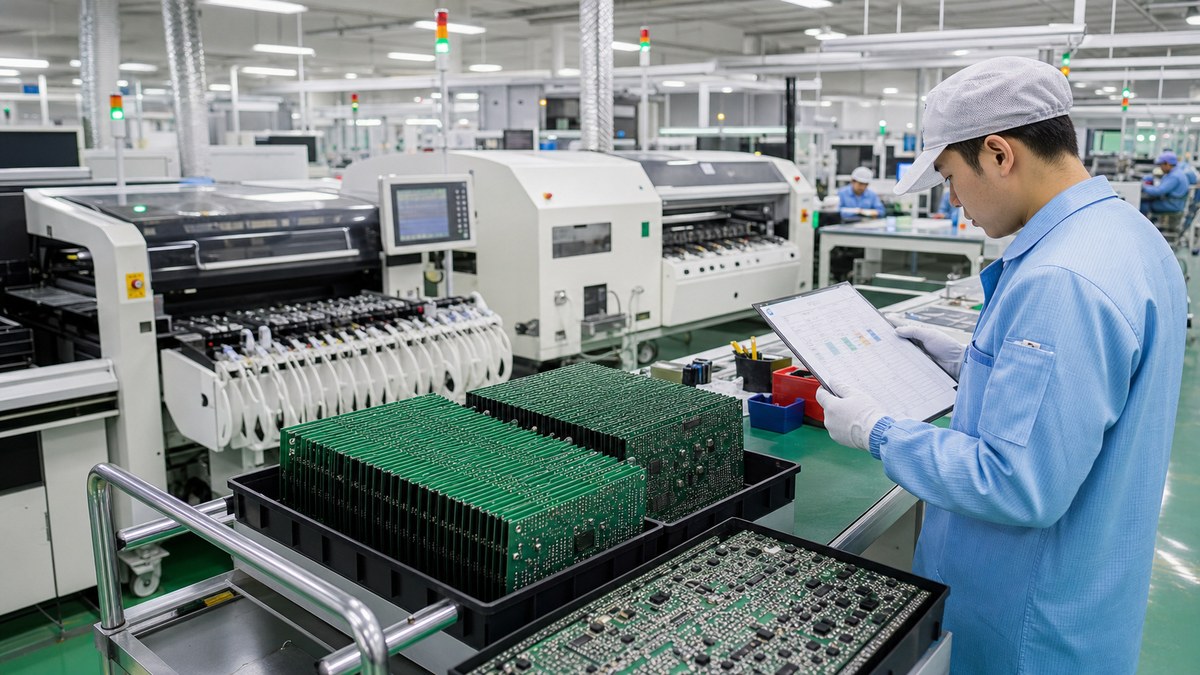
EBest Circuit directly serves USA buyers that need PCB fabrication, PCBA service, BOM/CPL review, DFM review, component sourcing, inspection and production planning in one RFQ path.
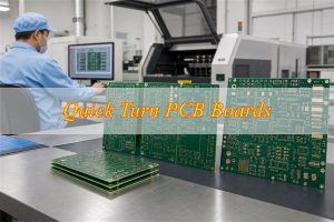
Before choosing a quick turn PCB supplier, check what can slow the order after the quote looks fast.
Fast PCB projects usually fail in the small details. The buyer sees a short lead time, but the supplier may still need missing files, unclear stackup notes, unavailable parts, assembly clearance changes or test decisions before the job can move.
- The quote promises fast fabrication, but BOM/CPL review, PCBA, stencil, inspection, testing and freight are not included.
- The supplier accepts the files, but does not confirm material, stackup, copper, finish, drill limits, impedance, panelization or assembly clearance.
- A prototype lead time is quoted, but the supplier does not explain whether the same design can move into low-volume or repeat production.
- Components look available at first, but substitutes, MOQ, package mismatch or long-lead parts change the assembly schedule.
- The buyer receives one delivery date without knowing how much time belongs to file review, fabrication, sourcing, assembly, inspection and shipping.
EBest Circuit helps USA buyers turn a quick turn request into a checked PCB and PCBA plan.
- We review Gerber or ODB++ files, stackup, material notes, copper, finish, quantity, test needs and target delivery date before quote approval.
- We connect bare-board fabrication with PCBA service, BOM/CPL review, component sourcing, inspection and production planning.
- We help catch DFM questions early, so buyers can fix layout, panel, soldering, hole, material or assembly issues before the order is already running.
- We review sourcing risk before assembly, especially where substitutes, package availability or MOQ can change a fast schedule.
- We help compare prototype, low-volume and production routes so speed does not hide quality, cost or delivery risk.
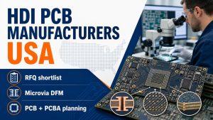
Top 12 Quick Turn PCB Manufacturer USA Options for RFQs
Use this shortlist as a reference, then send every supplier the same files and the same scope questions. EBest Circuit is listed first because USA buyers can include us early when they want DFM, PCB fabrication, PCBA, BOM/CPL review and cost control checked together.
1. EBest Circuit
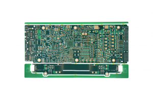
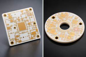
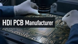
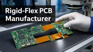
Main Products / PCB or PCBA Type: Rigid PCB, multilayer PCB, HDI PCB, flex PCB, PCBA, DFM and BOM/CPL review
Certifications: IATF 16949, ISO 9001, ISO 13485, UL, RoHS, REACH
Service Type: Prototype, low volume, production, PCB fabrication and PCBA
Location / Service Region: Directly serves USA buyers
2. AdvancedPCB
Main Products / PCB or PCBA Type: Quick turn PCB, prototype PCB, PCB fabrication and PCBA support
Certifications: Confirm ISO, UL and RoHS scope before RFQ
Service Type: Quick turn prototype, fabrication and assembly support
Location / Service Region: USA supplier option
3. Sierra Circuits
Main Products / PCB or PCBA Type: Quickturn PCB prototype, PCB fabrication, assembly and components
Certifications: ISO 9001:2015, ISO 13485:2016, UL, RoHS, REACH
Service Type: Prototype, quick turn, production PCB and assembly
Location / Service Region: California, USA
4. PCB Unlimited
Main Products / PCB or PCBA Type: USA quickturn PCBs, prototype PCB, low-volume PCB and PCB assembly support
Certifications: Confirm ISO, UL and RoHS scope before RFQ
Service Type: Quick turn prototype and low-volume PCB support
Location / Service Region: USA service option
5. Sunstone Circuits
Main Products / PCB or PCBA Type: Quick-turn PCB, prototype PCB, production PCB and PCB design support
Certifications: Confirm ISO, UL and RoHS scope before RFQ
Service Type: Quick turn prototype and production PCB services
Location / Service Region: Oregon, USA
6. Green Circuits
Main Products / PCB or PCBA Type: Quick turn PCB assembly, prototype PCB services and production assembly
Certifications: Confirm ISO and customer-required documentation scope before RFQ
Service Type: Quick turn PCBA, prototype and production assembly
Location / Service Region: California, USA
7. Cirexx International
Main Products / PCB or PCBA Type: Quick turn PCB fabrication, prototype PCB and complex PCB support
Certifications: Confirm ISO, UL and process documentation scope before RFQ
Service Type: Quick turn fabrication and prototyping
Location / Service Region: California, USA
8. Rush PCB
Main Products / PCB or PCBA Type: Quick turn PCB, rigid PCB, flex PCB, prototype PCB and assembly
Certifications: Confirm ISO, UL and RoHS scope before RFQ
Service Type: Prototype, quick turn and assembly support
Location / Service Region: California, USA
9. Bay Area Circuits
Main Products / PCB or PCBA Type: Quick turn PCB fabrication, prototype PCB and design support
Certifications: Confirm ISO, UL and inspection documentation scope before RFQ
Service Type: Quick turn fabrication and prototype support
Location / Service Region: California, USA
10. Avanti Circuits
Main Products / PCB or PCBA Type: Quick turn PCB fabrication and custom printed circuit boards
Certifications: Confirm ISO, UL and project documentation scope before RFQ
Service Type: Quick turn prototype and fabrication services
Location / Service Region: Arizona, USA
11. San Francisco Circuits
Main Products / PCB or PCBA Type: Prototype PCB, quick turn PCB, fabrication and assembly support
Certifications: Confirm ISO, UL and customer-required records before RFQ
Service Type: Prototype, quick turn fabrication and assembly support
Location / Service Region: California, USA
12. American Standard Circuits
Main Products / PCB or PCBA Type: Quick turn PCB, rigid PCB, flex PCB, rigid-flex PCB, RF and metal-backed PCB
Certifications: Confirm ISO, AS9100, UL and project-specific scope before RFQ
Service Type: Quick turn, prototype and production PCB manufacturing
Location / Service Region: Illinois, USA
What Quick Turn PCB Really Means Before You Order
Quick turn means the supplier can compress the review, fabrication and delivery path, but it does not remove engineering work. If the design has unclear requirements, a fast quote can still become slow once production questions appear.
| Fast Promise | What It Usually Means | What the Buyer Should Confirm |
|---|---|---|
| 24-hour or same-day quote | The supplier can price standard files quickly. | Ask whether DFM review, stackup checks and assembly scope are included. |
| Fast bare-board fabrication | The PCB can be built quickly after files are accepted. | Confirm layer count, material, finish, copper, drill and test limits. |
| Quick turn PCBA | Assembly is planned quickly after BOM/CPL review. | Confirm component availability, substitute approval, stencil, AOI, X-ray and functional test. |
| Fast delivery | The supplier can ship quickly after build completion. | Ask for separate timing for file review, fabrication, sourcing, assembly, inspection and shipping. |
Quick Turn PCB Fabrication vs Quick Turn PCB Assembly
Fabrication speed and assembly speed are two different checks. A supplier may build bare boards quickly but still need time to source components, prepare stencil data, verify CPL coordinates, inspect solder joints and run functional tests.
| Scope | What Happens | Buyer Check |
|---|---|---|
| PCB fabrication | The bare board is manufactured from Gerber or ODB++ data. | Confirm material, stackup, finish, copper, holes, impedance and electrical test. |
| PCB assembly | Components are placed and soldered on the board. | Confirm BOM/CPL, component sourcing, stencil, AOI, X-ray, rework and test plan. |
| Turnkey quick turn | Fabrication, sourcing, assembly and inspection are connected. | Ask what is included, what can delay the order and how changes are approved. |
Need a Fast PCB Quote Without Guessing the Real Build Risk?
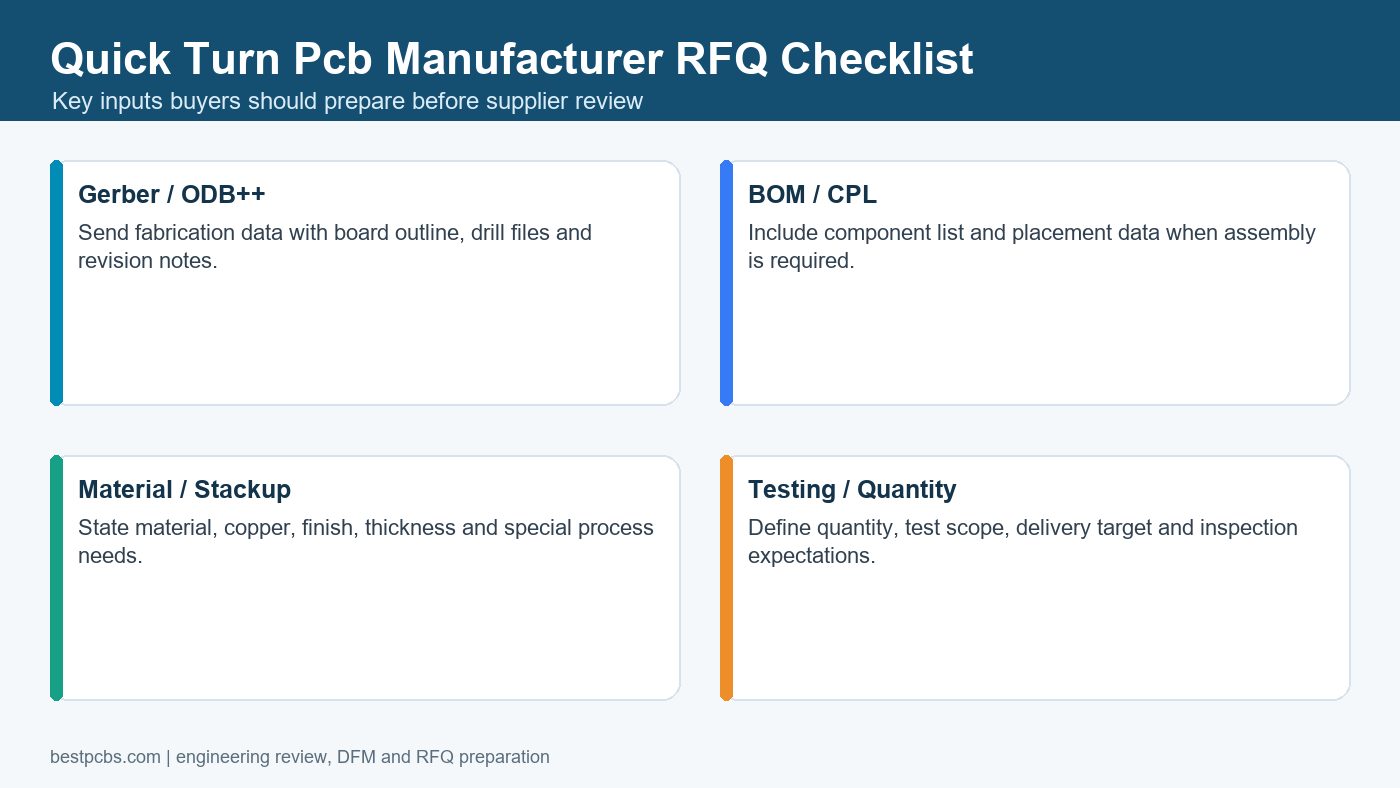
Send Gerber or ODB++ files, BOM/CPL, quantity, material notes, finish and test requirements. EBest Circuit can check DFM, PCB fabrication, PCBA, sourcing, inspection and delivery assumptions before speed creates expensive surprises.
Gerber | ODB++ | BOM/CPL | Fast Quote | PCBA | Inspection
Files That Decide Whether a Fast PCB Quote Is Real
A fast quote is only as reliable as the file package behind it. Missing drill data, unclear finish notes, an incomplete BOM or a wrong CPL can turn a quick build into email back-and-forth.
- Gerber or ODB++ files and NC drill files.
- Stackup, material, board thickness, copper weight and surface finish notes.
- Quantity, target delivery date, delivery destination and expected repeat quantity if known.
- BOM and CPL if assembly is required.
- Assembly drawing, polarity notes, test requirements and any special packing requirement.
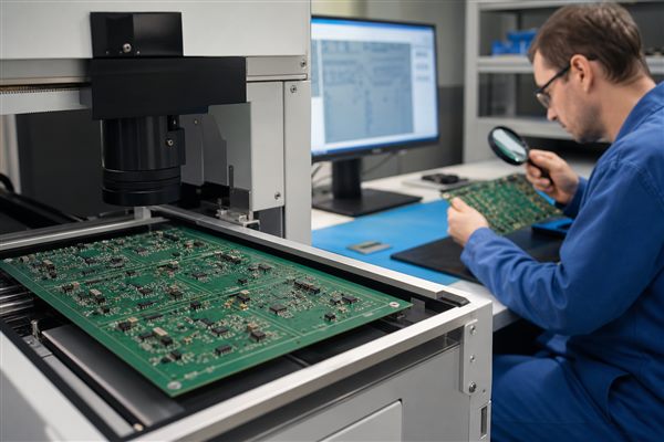
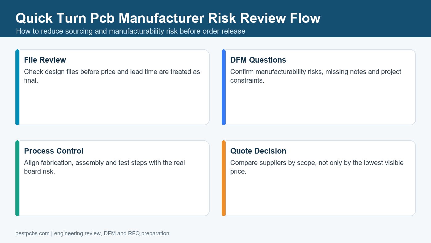
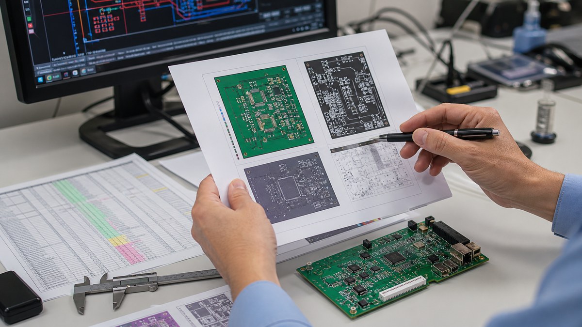
DFM Checks That Protect a Quick Turn Schedule
DFM review is what keeps speed from turning into rework. A supplier should check whether the board can actually be fabricated and assembled under the requested timing before the order is released.
Step 1: Check fabrication limits such as spacing, hole size, annular ring, copper, solder mask and finish.
Step 2: Check assembly limits such as component clearance, polarity, package size, stencil needs and test access.
Step 3: Confirm unclear items before the quote is approved, not after the build has already started.
Step 4: Decide whether the order is a prototype-only build or a first step toward low-volume production.
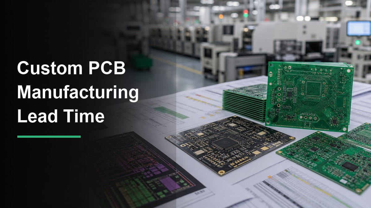
Lead-Time Planning for Quick Turn PCB and PCBA Orders
Lead time should be broken into stages so the buyer can see where time can be lost. The fastest supplier is not the one with the shortest slogan; it is the one that explains the full path clearly.
Certifications and Quality Records to Confirm on Fast Orders
Speed does not replace quality documentation. Buyers should confirm whether the certificate, inspection and test records match the quoted board type, assembly process and end-use requirement.
- Confirm ISO, UL, RoHS, REACH, IATF, AS9100 or medical-quality requirements when they apply to the project.
- Ask whether records apply to fabrication, assembly, testing or only part of the service.
- Request electrical test, AOI, X-ray, first-article or material records when the project needs them.
- If a supplier page lists a certificate name, confirm the facility and service scope before purchase approval.
Prototype, Low-Volume and Production Quick Turn Choices
A quick prototype should be planned with the next build in mind. If the first order is only treated as a one-time sample, the buyer may repeat the same questions when moving into low-volume production.
| Order Stage | Main Risk | What to Ask |
|---|---|---|
| Prototype | The design may still need changes. | Can you return specific DFM and assembly comments before fabrication starts? |
| Low volume | Sourcing, setup and inspection become more visible. | Can PCB, PCBA and test assumptions be separated in the quote? |
| Production | Repeatability and documentation matter more than first-sample speed. | How will repeat builds, quality records and delivery changes be controlled? |
USA Quick Turn Supplier vs EBest Circuit: What Buyers Should Compare
The right comparison is not just location or speed, but how much of the project risk is checked before you commit. EBest Circuit should be compared early when the buyer needs fabrication, PCBA, sourcing, testing and delivery assumptions reviewed together.
| Comparison Point | Typical Supplier Question | EBest Circuit RFQ Advantage |
|---|---|---|
| Engineering response | Does the supplier review files before quoting or only price the upload? | We review DFM, fabrication, BOM/CPL, PCBA and test assumptions together. |
| Cost visibility | Are assembly, sourcing, inspection and freight included or added later? | We help separate fabrication, component, assembly, testing and delivery assumptions. |
| Production path | Can the first build move into low-volume or repeat production? | We plan prototype, low-volume and production routes before the order is locked. |
| Buyer action | Can the supplier tell you exactly what to send next? | USA buyers can send Gerber/ODB++, BOM, CPL, quantity, finish and target date for review. |
Quote Gaps That Make Quick Turn PCB Orders Expensive
A fast quote can become expensive when important work is left outside the first price. Buyers should compare the full order scope instead of choosing the shortest quoted lead time.
| Quote Gap | What Can Happen | Better RFQ Question |
|---|---|---|
| Bare-board only | PCBA and sourcing appear later as separate cost. | Does this quote include assembly, stencil, inspection and test? |
| Unclear BOM | Substitutes or MOQ change cost and schedule. | Can you review the BOM before final quote approval? |
| No test plan | A board can look good but fail electrically or functionally. | Which inspection or test method is recommended? |
| One delivery number | Fabrication may be fast while components or assembly delay the order. | Can you break lead time into review, fabrication, assembly and shipping? |
Why EBest Circuit Should Be Compared Early
EBest Circuit should be in the first RFQ round because we help buyers see the real build path before speed creates avoidable cost, rework or delivery surprises. USA buyers get more value when DFM, BOM/CPL, fabrication, PCBA, inspection and delivery are reviewed together.
- Engineering response: We review Gerber or ODB++ data, stackup notes, material, finish, copper and manufacturability before production starts.
- PCBA support: We connect BOM/CPL review, component sourcing, SMT assembly, inspection and testing with the bare PCB plan.
- Cost control: We help identify quote gaps before they become extra cost after order approval.
- Production planning: We help buyers think beyond the first fast sample and prepare for low-volume or repeat production.
Frequently Asked Questions About Quick Turn PCB Manufacturer USA Options
What is a quick turn PCB manufacturer?
A quick turn PCB manufacturer is a supplier that can quote, review and build PCB orders faster than a standard production path. Buyers still need to confirm files, materials, DFM, inspection and delivery details before trusting the lead time.
Is quick turn PCB fabrication the same as quick turn PCB assembly?
No. Fabrication builds the bare board, while assembly places and solders components. A fast bare-board quote does not automatically include BOM/CPL review, sourcing, stencil, AOI, X-ray or functional testing.
What files are needed for a quick turn PCB quote?
Send Gerber or ODB++, NC drill, stackup, material, finish, copper, quantity, BOM, CPL and test requirements. Complete files reduce back-and-forth and make the quoted lead time more realistic.
Why do quick turn PCB quotes vary so much?
Quotes vary because suppliers may include different scopes. One quote may cover only bare boards, while another includes DFM, PCBA, sourcing, inspection, testing and delivery planning.
Can EBest Circuit support USA quick turn PCB buyers?
Yes. EBest Circuit directly serves USA buyers with PCB fabrication review, PCBA planning, BOM/CPL review, component sourcing, inspection and delivery planning. Buyers can send files early for RFQ review.
How can I avoid delays on a quick turn PCB order?
Ask for DFM and BOM/CPL review before the order starts. Delays often come from unclear stackup notes, missing drill files, unavailable components, assembly clearance issues or late test decisions.
Are certificates still important for quick turn PCB orders?
Yes. Fast orders still need the right quality records when the project requires them. Confirm whether certificates and inspection documents apply to the quoted facility, process and service scope.
Should I choose the fastest quoted lead time?
Not by itself. Choose the supplier that explains how the lead time is built. A clear supplier separates file review, fabrication, sourcing, assembly, inspection and shipping instead of giving only one number.
What makes a quick turn PCB supplier response trustworthy?
A trustworthy response explains uncertainty clearly. It should state what is manufacturable, what is unclear, what can change cost and what must be confirmed before fabrication or assembly begins.
When should I send files to EBest Circuit?
Send files before you approve the supplier shortlist. Early review gives time to catch DFM, BOM/CPL, sourcing, assembly and testing questions before they become expensive changes.
Before You Approve a Quick Turn PCB Order, Let Us Check the Full Scope
A fast promise is useful only when fabrication, BOM/CPL, PCBA, inspection, testing and delivery planning are clear. EBest Circuit helps USA buyers compare the real order path before purchase approval.
Gerber | ODB++ | BOM/CPL | Fast Quote | PCBA | Inspection
Final RFQ Recommendation
Do not choose a quick turn PCB manufacturer from speed claims alone. Send the same file package to each candidate, compare the quality of the engineering response, and put EBest Circuit in the first RFQ batch when you need PCB fabrication, PCBA, DFM, BOM/CPL, component sourcing, inspection and delivery planning checked together. Email Gerber/ODB++, BOM, CPL, quantity, material, surface finish, test requirements and target delivery date to sales@bestpcbs.com.