





Multilayer PCB manufacturing builds three or more conductive copper layers into one interconnected board. The factory images and etches the inner layers, inspects them, laminates cores and prepreg, drills the bonded panel, plates the holes, forms the outer circuits, applies protective finishes and tests the completed board. This construction creates routing density and controlled electrical structures that single- and double-sided boards cannot provide, but it demands tighter control of registration, resin flow, drilling, plating and documentation.
For engineers and buyers, layer count is only the visible headline. The real manufacturing risk comes from how the stackup, via structure, copper distribution, materials, finished thickness and tolerances interact. A practical review therefore needs to cover both the fabrication sequence and the design decisions that determine yield, reliability and lead time.

What Is Multilayer PCB Manufacturing?
Multilayer PCB manufacturing joins at least three patterned copper layers through dielectric materials and plated vias. Commercial rigid multilayer boards commonly begin at four layers because an even, symmetrical construction is easier to design and manufacture than many odd-layer arrangements.
Signal layers route functional connections, while selected inner layers may serve as ground or power planes. Their close relationship influences impedance, return-current paths, electromagnetic behavior and power distribution. The board is not produced by simply stacking finished double-sided PCBs: individual inner layers are formed and inspected before they become inaccessible inside the laminated structure.
Which Materials Form a Multilayer PCB Stackup?
Material selection in multilayer PCB manufacturing combines copper foil, cured laminate cores and partially cured prepreg. Solder mask and the selected surface finish protect the completed outer surfaces. Each material has a different job, and substitutions can change electrical or mechanical behavior.
| Stackup element | Manufacturing function | Review point |
| Copper foil | Forms traces, pads and planes | Starting and finished copper thickness, width, spacing and copper distribution |
| Core | Provides a cured dielectric with copper on one or both sides | Thickness, resin system, glass style, Tg and electrical properties |
| Prepreg | Bonds layers and fills spaces during lamination | Resin content, cured thickness, glass style and copper-feature fill |
| Solder mask | Protects outer circuitry and defines exposed pads | Registration, dams, clearance and assembly needs |
| Surface finish | Protects exposed copper and supports soldering or contact | Pad geometry, assembly process, storage and application |
Do not select a laminate using Tg alone. Dk, Df, z-axis expansion, moisture behavior, decomposition temperature and supplier data may matter depending on signal speed, thermal cycles, plated-hole reliability and operating environment. Any proposed equivalent material should be reviewed against the values that matter to the design.
How Does the Multilayer PCB Manufacturing Process Work?
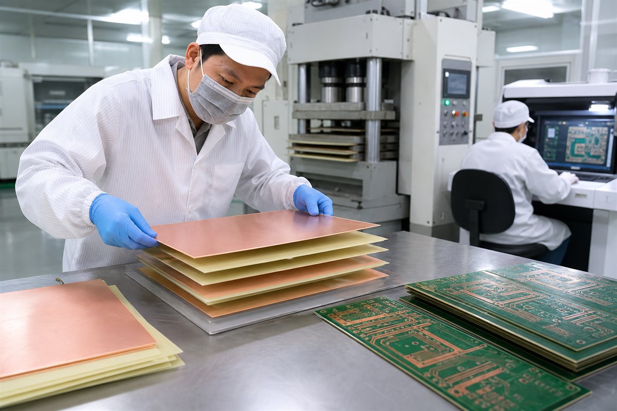
The multilayer PCB manufacturing process moves from data preparation to inner-layer formation, lamination, drilling, plating, outer-layer processing, finishing and testing. Exact sequencing varies with the via structure and production equipment, but the control logic remains consistent.
- Data and DFM review: Fabrication files are checked against the proposed stackup, drill structure, tolerances and process capability.
- Material preparation: Cores, copper foil and prepreg are selected, cut and identified for the production lot.
- Inner-layer imaging: Photoresist, exposure and development transfer the circuit pattern to copper-clad cores.
- Inner-layer etching: Unwanted copper is removed to create traces, pads and planes.
- Inner-layer AOI: Automated optical inspection checks opens, shorts, spacing and pattern defects before lamination.
- Surface treatment and lay-up: Inner layers are prepared for adhesion and stacked with prepreg and outer copper foil.
- Lamination: Heat, pressure and a controlled cycle bond the stack into one panel.
- Drilling and desmear: Mechanical or laser drilling forms holes; desmear removes resin residue and conditions hole walls.
- Copper deposition and plating: A conductive seed layer and electroplated copper create reliable hole-wall connections.
- Outer-layer imaging and etching: The external circuit patterns are formed and inspected.
- Solder mask and surface finish: Protective coating, markings and the specified pad finish are applied.
- Profiling and testing: Boards are routed or scored, electrically tested and inspected against release criteria.
Why Inner-Layer Imaging and AOI Are Critical
Inner-layer AOI is the last practical opportunity to reject many circuit defects before lamination hides them. Imaging determines the geometry of circuits that cannot be repaired easily after pressing. A missed open, short, pinhole or spacing error can compromise the entire laminated panel.
Artwork compensation may be required because materials and copper patterns respond to processing and lamination. Registration targets allow the factory to align layers and verify position. Dense routing, thin dielectric spacing and small annular rings reduce the available process margin, so the design and supplier should agree on achievable values rather than relying on nominal CAD dimensions alone.
What Happens During Multilayer PCB Lamination
Multilayer PCB lamination bonds copper-clad cores and prepreg with controlled heat, pressure and time. The prepreg resin flows, fills spaces around copper features and cures into the dielectric structure that holds the stack together.
The cycle must support adequate resin flow and cure without creating excessive squeeze-out, voids, layer movement or thickness variation. Heavy copper, uneven copper density and large resin-demand areas can make filling more difficult. Symmetrical stackups and balanced copper distribution help control stress and warpage, but the exact construction should still be confirmed by the fabricator.
Sequential-lamination HDI boards repeat parts of this process to create blind or buried structures. Each additional lamination cycle adds alignment, material and yield considerations that can extend engineering review and production lead time.
How Drilling, Desmear and Copper Plating Connect the Layers
Drilling, desmear and copper plating turn physical holes into reliable electrical connections between layers. Desmear exposes clean copper at the inner-layer interfaces before copper deposition and electroplating build the conductive hole wall.
The relationship between finished board thickness and finished hole diameter is often discussed as the via aspect ratio. Smaller holes in thick boards are harder to process and plate uniformly. Blind microvias introduce different geometry and may require laser drilling, filling and sequential lamination. Designers should confirm finished-hole requirements, plating assumptions and via structures with the manufacturer before release.
Poor desmear can leave resin that interferes with the connection to inner-layer copper. Inadequate or non-uniform plating can reduce the conductive cross-section. Inspection and test plans should be proportional to the board technology and reliability requirement.
Which Defects Threaten Multilayer PCB Yield and Reliability?
The most serious defects in multilayer PCB manufacturing can remain hidden inside the laminated structure or plated holes. Common risks include misregistration, opens or shorts, delamination, resin voids, poor hole-wall plating, inner-layer separation, bow and twist, and impedance deviation. Each defect has a different origin and prevention method.
| Risk | Possible contributor | Preventive control |
| Layer misregistration | Material movement, alignment or compensation error | Registration tooling, process compensation and annular-ring margin |
| Delamination or voiding | Moisture, contamination, weak adhesion or poor resin fill | Material handling, surface preparation and validated lamination cycle |
| Plating void or thin copper | Poor hole conditioning or non-uniform plating | Desmear control, bath control, coupon review and inspection |
| Open or short circuit | Imaging, etching, contamination or handling defect | AOI, process control and electrical testing |
| Excessive bow or twist | Asymmetrical stackup, copper imbalance or thermal stress | Balanced construction, panel engineering and controlled processing |
| Impedance outside tolerance | Trace geometry, copper, dielectric or etch variation | Stackup approval, controlled process and impedance coupons |
How Are Multilayer PCBs Inspected and Tested?
Inspection and testing in multilayer PCB manufacturing combine in-process checks with final electrical and dimensional verification. No single method detects every failure mode, so the control plan should match the layer count, via technology, tolerances and end-use risk.

- AOI: Inner- and outer-layer inspection checks patterned copper before later operations hide or cover it.
- Electrical test: Continuity and isolation are verified against the netlist.
- Microsection: Representative coupons can reveal plated-hole structure, copper thickness and internal interfaces.
- Impedance verification: Test coupons can confirm controlled-impedance structures when specified.
- Dimensional inspection: Thickness, holes, routing and drawing requirements are measured.
- Visual inspection: Solder mask, surface finish, markings and workmanship are checked.
Acceptance criteria should be agreed before production. If a particular IPC class, test report, coupon, traceability record or reliability test is required, include it in the request for quotation rather than adding it after fabrication begins.
What Affects Multilayer PCB Manufacturing Lead Time?
Lead time depends on the complete fabrication package, not layer count alone. Material availability, process complexity, testing requirements and design stability determine how quickly engineering review and production can move forward.
- Panel complexity: Layer count, panel utilization and board dimensions
- Material readiness: Laminate family, availability and requested brand
- Copper and thickness: Finished thickness, copper weight and heavy-copper features
- Circuit geometry: Fine lines, tight spacing and small annular rings
- Drilling demand: Small finished holes and high aspect ratios
- Via architecture: Blind, buried, stacked or filled vias and sequential lamination
- Controlled features: Impedance structures and tight dimensional tolerances
- Final processing: Surface finish, edge plating and special mechanical work
- Verification scope: Testing, coupons, reports and traceability requirements
- Release planning: Order quantity, revision stability and requested schedule
A design that stays within stable production rules is easier to release and repeat than a nominally simpler board that pushes several capability limits. Ask for DFM feedback before locking the stackup and via architecture, especially when a prototype will later move to volume production.
How Should a Design Be Prepared for Multilayer PCB Manufacturing?
A manufacturable multilayer PCB design provides consistent data and leaves enough process margin for the selected technology. Start the stackup discussion before final routing when impedance, high-speed return paths, thickness or complex vias matter.
- Stackup symmetry: Use a balanced layer construction where the electrical design permits it.
- Copper balance: Follow supplier guidance for thieving or copper fill in large open areas.
- Finished copper: Define the final value, not only the starting foil, where the distinction matters.
- Impedance data: Identify controlled nets and provide target values and tolerances.
- Clearance rules: Confirm drill-to-copper, annular-ring, slot and edge requirements.
- Via discipline: Avoid unnecessary via types or lamination cycles.
- Drawing consistency: Keep fabrication notes aligned with Gerber or ODB++ data.
- Revision control: Freeze fabrication, drill, netlist and assembly files together.
Use the design condition—not a single nominal dimension—to decide what the fabricator must confirm before release. The following matrix turns common multilayer-board choices into specific engineering and purchasing checks.
| Design condition | Primary manufacturing risk | Confirm before release |
| High layer count or increased finished thickness | Registration loss, thickness variation and reduced plated-hole process margin | Approved stackup, finished-thickness tolerance, minimum finished hole and aspect ratio |
| Fine lines combined with heavier finished copper | Over-etching, spacing loss and non-uniform conductor geometry | Finished copper definition, achievable line and spacing, and outer-layer plating allowance |
| Small plated holes in a thick board | Incomplete desmear, plating voids or thin hole-wall copper | Finished-hole diameter, drill allowance, aspect ratio, plating requirement and microsection scope |
| Controlled-impedance routing | Impedance shift caused by dielectric, copper or etch variation | Target impedance, tolerance, reference layer, trace geometry, material properties and coupon plan |
| Blind, buried, stacked or filled vias | Additional lamination cycles, alignment risk and unclear fill requirements | Via span, stacking or staggering, fill type, copper cap, planarization and sequential-lamination plan |
| Large copper-free areas or uneven plane density | Resin-flow imbalance, thickness variation, plating non-uniformity or bow and twist | Copper-balancing method, clearance constraints, panel orientation and acceptable bow and twist |
Multilayer PCB Case Analysis: From Design Requirements to Production Output
This representative, non-customer-specific multilayer PCB manufacturing case shows how a design can move from technical requirements to a controlled production package. It uses values within the supplied rigid-board capability table and does not claim a named customer, measured yield or field-performance result.
Project background
The example is a 10-layer industrial control board that combines dense digital routing, dedicated power and ground planes, controlled-impedance nets and connectors that must align with an existing enclosure. The prototype is intended to become the reference build for repeat production.
Project requirements
- Board construction: 10 layers, 1.6 mm finished thickness and a symmetrical high-Tg FR-4 stackup.
- Circuit geometry: 1 oz inner and outer copper with 4/4 mil minimum line and spacing.
- Hole structure: 0.20 mm minimum finished plated holes within an 8:1 through-hole aspect ratio.
- Electrical control: Defined impedance targets, reference planes and coupon requirements.
- Final verification: ENIG surface finish, electrical test, dimensional inspection and agreed quality records.
Engineering solution
- Stackup review: Check symmetry, dielectric selection, copper balance and impedance feasibility before routing is frozen.
- DFM closure: Review annular rings, drill-to-copper clearance, panel utilization and fabrication-note consistency.
- Prototype control: Use the first build to verify dimensions, hole structure, impedance evidence and assembly fit.
- Release control: Freeze fabrication, drill, netlist, BOM, placement and test files under one approved revision.
Output result
The defined output is a revision-controlled prototype and production package containing the approved stackup, closed DFM actions, fabrication data, inspection requirements and test records. Actual electrical, assembly and field results must be confirmed from the manufactured project rather than inferred from this representative example.
What Multilayer PCB Services Does EBest Circuit Provide?
EBest Circuit provides coordinated support from design review and prototyping through production, sourcing and assembly. Keeping the release package under one engineering workflow reduces revision mismatches between bare-board and assembly data.
- PCB design and DFM: Review stackup symmetry, materials, finished copper, via architecture, impedance structures and fabrication notes.
- Prototype verification: Confirm thickness, hole structure, impedance, assembly fit and inspection evidence before production release.
- Mass production: Control revisions, materials, repeatability, traceability and inspection requirements across production lots.
- Component sourcing: Coordinate BOM availability, approved alternatives and component changes with the assembly release.
- PCB assembly: Review land patterns, surface finish, panel format, placement data, programming method and test plan.
What Are EBest Circuit’s Multilayer PCB Manufacturing Capabilities?
EBest Circuit’s supplied rigid-board capability table separates preferred production limits from special-process limits. Special-process values require an engineering review of the complete stackup, panel design, copper distribution and acceptance criteria.
| Capability item | Standard process | Special process | Engineering note |
| FR-4 layer count | 1-10 layers; high-Tg material required from 8 layers | 10-32 layers | Final feasibility depends on stackup, thickness, via structure and registration margin. |
| Inner-layer copper | 0.5-5 oz | 5-20 oz | Heavier copper requires wider conductors and spacing plus adequate resin fill. |
| Outer-layer copper | 1-5 oz | 5-20 oz | Finished copper should be stated clearly because plating affects final geometry. |
| Minimum finished hole | 0.20 mm | 0.15 mm | Review drill size together with finished thickness and required plating. |
| Through-hole aspect ratio | 8:1 | 10:1 | Lower ratios generally provide a wider plating process margin. |
| Inner-layer line/space at 1 oz | 4/4 mil | 3/3 mil | Copper weight changes the achievable line and spacing values. |
| Outer-layer line/space at 1 oz | 4/4 mil | 3/3 mil | Do not apply the 1 oz rule to heavier finished copper without review. |
| Processed board thickness | Typically 0.4-3.5 mm, depending on surface finish; hard-gold-finger combinations start at 1.0 mm | Nonstandard thicknesses above 0.15 mm and below 8.0 mm require review | Layer count, panel size and surface finish can narrow the usable range. |
| Available surface finishes | OSP, HASL, ENIG, immersion silver, immersion tin, ENEPIG and hard gold fingers | Combination finishes subject to review | Select the finish around assembly, contact, shelf-life and application requirements. |
Capability limits should never be evaluated one row at a time. A design may meet the individual line, hole and layer-count limits yet still require special processing when those limits occur together. Submit the actual fabrication data for DFM confirmation before treating a stated maximum as a production commitment.
Why Choose EBest Circuit for Multilayer PCB Manufacturing?
Choose EBest Circuit when the project needs engineering review, transparent process limits and coordinated support from prototype through assembly. The final sourcing decision should still be based on the actual stackup, via structure, inspection plan and acceptance criteria.
- Engineering-led DFM: Review stackup, via structure, copper geometry and special-process requirements before production release.
- Transparent capability limits: Separate standard production windows from values that require additional engineering confirmation.
- Material and traceability control: Align laminate selection, approved alternatives and required lot records with the purchase specification.
- Inspection planning: Coordinate AOI, electrical test, microsection, impedance and report requirements around product risk.
- Integrated project support: Connect design review, prototyping, production, component sourcing and PCB assembly within one release workflow.
- Revision-matched quotation: Review the same fabrication files, specifications and acceptance criteria used for production.
For available build options and supplier support, review EBest Circuit’s multi-layer PCB fabrication capabilities, then submit the actual production files for confirmation.
What Files Are Needed for a Multilayer PCB Quote?
An accurate multilayer PCB manufacturing quote requires one complete, revision-matched fabrication package. Include Gerber or ODB++ data, NC drill files, a fabrication drawing, stackup information, quantity and any controlled-impedance, testing, material or documentation requirements. Assembly quotations also require a BOM and pick-and-place data.
State the finished board thickness, copper requirements, surface finish, smallest finished hole, special vias, tolerances, panel or delivery format and intended production volume. If the stackup is not final, explain the electrical constraints and ask the supplier to propose a manufacturable construction rather than silently assuming a generic stackup.
Frequently Asked Questions About Multilayer PCB Manufacturing
Q1: Can an odd-layer multilayer PCB be manufactured?
A1: Yes, but an even, symmetrical construction is usually preferred. An odd-layer design may need an additional nonfunctional copper layer or a revised stackup to improve dimensional and thermal balance.
Q2: When should high-Tg laminate be specified?
A2: Consider high-Tg material when the board will face higher assembly temperatures, repeated thermal cycles or demanding service conditions. Tg alone does not define reliability; decomposition temperature, expansion behavior and the full laminate system also matter.
Q3: Should laminate substitutions be allowed on the fabrication drawing?
A3: Allow substitutions only through a defined approval process. The alternative should match the required electrical, thermal, mechanical and compliance properties, especially for controlled-impedance or qualification-sensitive products.
Q4: When is via filling required?
A4: Via filling may be needed for via-in-pad structures, stacked microvias, planar assembly surfaces or specific thermal paths. State the fill type, planarization and copper-cap requirements instead of using the word “filled” without a process definition.
Q5: When should back drilling be considered?
A5: Back drilling is useful when unused plated-through-hole stubs could affect high-speed signal integrity. The drawing should define the target layers, residual stub requirement, drill tolerance and any coupon or inspection expectation.
Q6: Does panelization need to be finalized before the first prototype?
A6: Not always, but early panel discussion helps uncover edge clearance, tooling, breakaway and assembly-handling constraints. The volume-production panel should be reviewed again when board outline, assembly method or production quantity changes.
Q7: Should bare multilayer PCBs be baked before assembly?
A7: Baking is not an automatic requirement for every board. Decide from moisture exposure, storage history, laminate guidance, surface finish and the assembly profile; unnecessary baking can also affect solderability or materials.
Q8: How should engineering changes be controlled after prototype approval?
A8: Release changes through a documented revision process covering fabrication data, drill files, drawings, stackup, BOM, placement data and test files. Mixing revisions is a common and preventable source of production errors.
Q9: Which production records should a buyer request?
A9: Request only records that support the product risk and acceptance plan. Useful options can include electrical-test confirmation, impedance results, microsection evidence, material traceability and inspection reports.
Q10: How should unused internal copper areas be handled?
A10: Coordinate copper thieving or balancing with the fabricator when large empty areas could affect plating uniformity, resin flow or dimensional stability. Any added copper must preserve electrical clearance and the intended plane behavior.
Summary
Multilayer PCB manufacturing succeeds when the stackup, materials, copper geometry, via structure and acceptance criteria are treated as one production system. Inner-layer AOI protects the build before lamination; controlled drilling, desmear and plating create reliable interconnections; final inspection verifies the finished result. Early DFM review reduces avoidable schedule and yield risk.
If you are sourcing multilayer PCB fabrication or PCBA support, contact EBest Circuit at sales@bestpcbs.com. For a faster engineering review and a more accurate quotation, submit Gerber or ODB++, NC drill files, BOM, quantity, approved or proposed stackup, assembly scope, firmware or programming method, test requirements and required quality documentation.
You may also like







Tags: multilayer PCB fabrication, multilayer PCB manufacturing, multilayer PCB process, Multilayer PCB Stackup