PCB manufacturing PCB manufacturing
Home > Blog

PCBA

Custom PCB Design for Mining: Dust, Vibration and Power Checks
Monday, July 13th, 2026
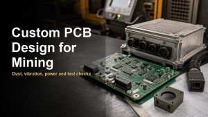
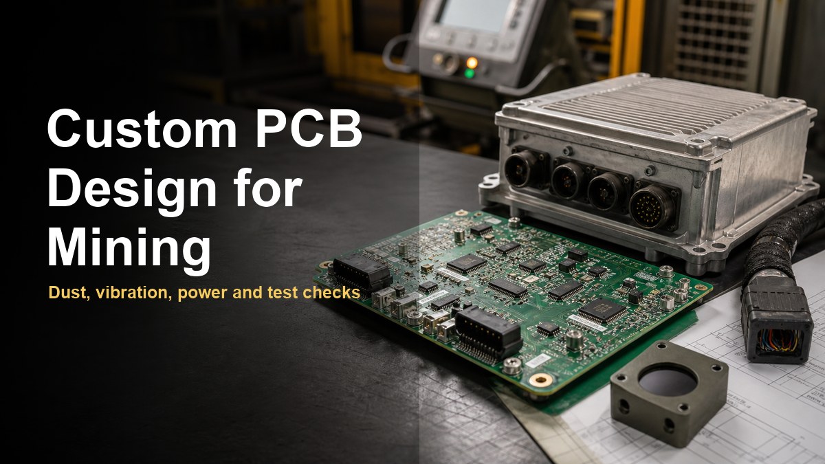
Custom PCB design for mining equipment with rugged enclosure and connector harness

Custom PCB design for mining equipment should be reviewed around dust, moisture, vibration, protected power input, connector strain relief, thermal control, test points and production-ready RFQ files. A mining electronics board is not only a circuit layout. It is part of a rugged system that may sit near motors, pumps, sensors, conveyors, vehicles, lighting, chargers or communication devices where contamination, shock and repair access matter.

This guide is written for engineers and buyers preparing a custom PCB or PCBA for mining-related equipment. It focuses on practical design and manufacturing checks before fabrication or assembly. If the product will be used underground, near combustible dust, or in another regulated hazardous area, confirm the applicable equipment-level certification requirements with your compliance team. A PCB supplier can support design for reliability, traceability and production quality, but board fabrication alone does not certify the complete mining device.

What does custom PCB design for mining need to solve?

Mining PCB design needs to keep electrical performance stable while the board is exposed to dust, vibration, heat, moisture, long cable runs and maintenance stress. The exact risks depend on whether the board is used in a sensor node, motor controller, lighting module, communication gateway, battery system, display panel or test device.

For a simple monitoring module, the main issues may be enclosure fit, connector sealing and low-power reliability. For a power or drive-related board, the review moves toward copper weight, creepage and clearance, thermal paths and protection components. Compact control electronics may also need an HDI PCB if the enclosure is tight and the component density is high.

Mining design risk PCB or PCBA check Why it matters
Dust and moisture Enclosure interface, coating decision, connector sealing and cleaning process Contamination can create leakage paths, corrosion and intermittent faults
Vibration and shock Mounting holes, board support, connector retention and heavy component placement Loose connectors or cracked solder joints can stop equipment in the field
Power variation Input protection, grounding, copper width, fusing and transient protection Long cables and inductive loads can create voltage stress
Heat buildup Copper weight, thermal vias, enclosure contact and material selection Sealed boxes often have limited airflow
Maintenance Test points, labels in drawings, harness plan and replaceable modules Field teams need faults isolated quickly without damaging the board

Where are custom mining PCBs used?

Custom mining PCBs are common in control, sensing, communication, lighting, power conversion and equipment monitoring devices. A buyer should define the use case before asking for a quote, because a sensor interface board and a high-current control board need different materials, copper rules and test plans.

Typical examples include conveyor monitoring electronics, pump controllers, battery management devices, rugged displays, LED lighting modules, wireless gateways, environmental sensors and vehicle-mounted control units. Some designs use standard FR4 PCB construction. Others need heavier copper, higher Tg material, metal-backed structures, conformal coating, sealed box integration or full PCBA support.

How should dust, moisture and enclosure fit be handled?

The PCB should be designed together with the enclosure, gasket, connector system and cleaning/coating plan. Treating the board as a flat electrical drawing and the enclosure as a later mechanical decision often creates failures at cable entries, mounting bosses, edge clearance and service access.
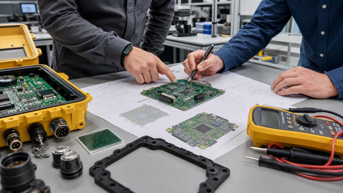
Engineers reviewing a rugged mining equipment PCB with enclosure gasket and connector samples
Mining electronics should be reviewed as a board, enclosure, connector and testable assembly, not as a bare PCB only.

Before layout release, check the board outline against the enclosure drawing, connector keepout area, mounting-hole tolerance, coating keepout, service connector position and any pressure-equalization or sealing requirement. If conformal coating is planned, mark no-coat areas around connectors, switches, programming pads and test contacts. If potting is planned, confirm component height, thermal behavior and repair expectations before the production file is frozen.

What vibration checks matter before production?

Vibration risk is controlled by board support, connector retention, solder joint protection and heavy component placement. A mining PCB can pass an electrical review and still fail in the field if a large inductor, terminal block, relay, transformer, battery connector or harness load is not mechanically supported.

Use larger mounting margins around high-stress areas. Keep heavy parts away from unsupported board edges when possible. Add strain relief for harnesses instead of letting cable pull act directly on solder joints. For mixed SMT and through-hole designs, define whether wave soldering, selective soldering or hand operations are expected. If the design includes high-current terminals, compare the copper and spacing assumptions against a relevant design reference such as the Heavy Copper PCB Design Guide.

How should power input and heat be reviewed?

Power input review should cover voltage range, surge exposure, reverse polarity risk, grounding, heat flow and copper current capacity. Mining equipment often connects through long cables, battery systems, motors, relays, lighting modules or chargers. These conditions can put more stress on input circuits than a clean lab supply.

For early DFM, send the supplier the expected operating voltage, maximum current, copper weight, target temperature range, board thickness, surface finish and any thermal interface to the enclosure. Do not ask for only a bare board price if the real product needs heat-spreading, coated assembly, heavy connectors or functional testing. The quote should reflect the way the board will be used.

Design area Questions to answer before RFQ
Input power What voltage range, current load, fuse strategy and reverse-polarity protection are required?
Grounding How are chassis ground, signal ground and shield termination handled?
Thermal path Will heat leave through copper pours, vias, thermal pads, an enclosure wall or a heatsink?
Copper weight Are high-current traces sized for the real load and temperature rise target?
Protection Are surge, ESD and inductive switching risks reviewed at cable and connector interfaces?

Which materials and stackups fit mining electronics?

The material choice should follow the electrical load, enclosure temperature, vibration risk and required board density. FR4 is often suitable for control and sensor boards, but high-current, high-heat or compact assemblies may need different copper, laminate, via and thermal decisions.

For dense signal boards, HDI can reduce routing congestion and help fit a smaller rugged enclosure. For power boards, thicker copper, larger spacing and thermal planning may matter more than density. For LED lighting or heat-generating modules, metal-backed or direct thermal path designs may be considered. The right choice depends on the project files, not on a generic mining label.

How should assembly and sourcing be planned?

Mining PCBA planning should include component availability, substitute approval, coating or sealing steps, test fixture needs and final box-level handling. A bare PCB schedule does not describe the finished product if the order also needs SMT, through-hole assembly, wiring, enclosure fit or functional testing.

Before releasing the order, provide a controlled BOM, approved alternates, centroid file, assembly drawing, polarity notes, connector orientation, firmware loading requirement and test criteria. If long-life parts or industrial-grade components are required, discuss Component Sourcing early. If the supplier is expected to deliver a mounted board in a sealed housing, treat it as a Box Build Assembly discussion rather than a normal PCB-only purchase.

What test plan should be ready before release?

The test plan should prove the board can be built, inspected and checked consistently before it reaches the field. At minimum, define electrical test for bare boards, AOI or visual inspection for assembly, functional checks for powered boards and any project-specific connector, LED, sensor, relay or communication test.
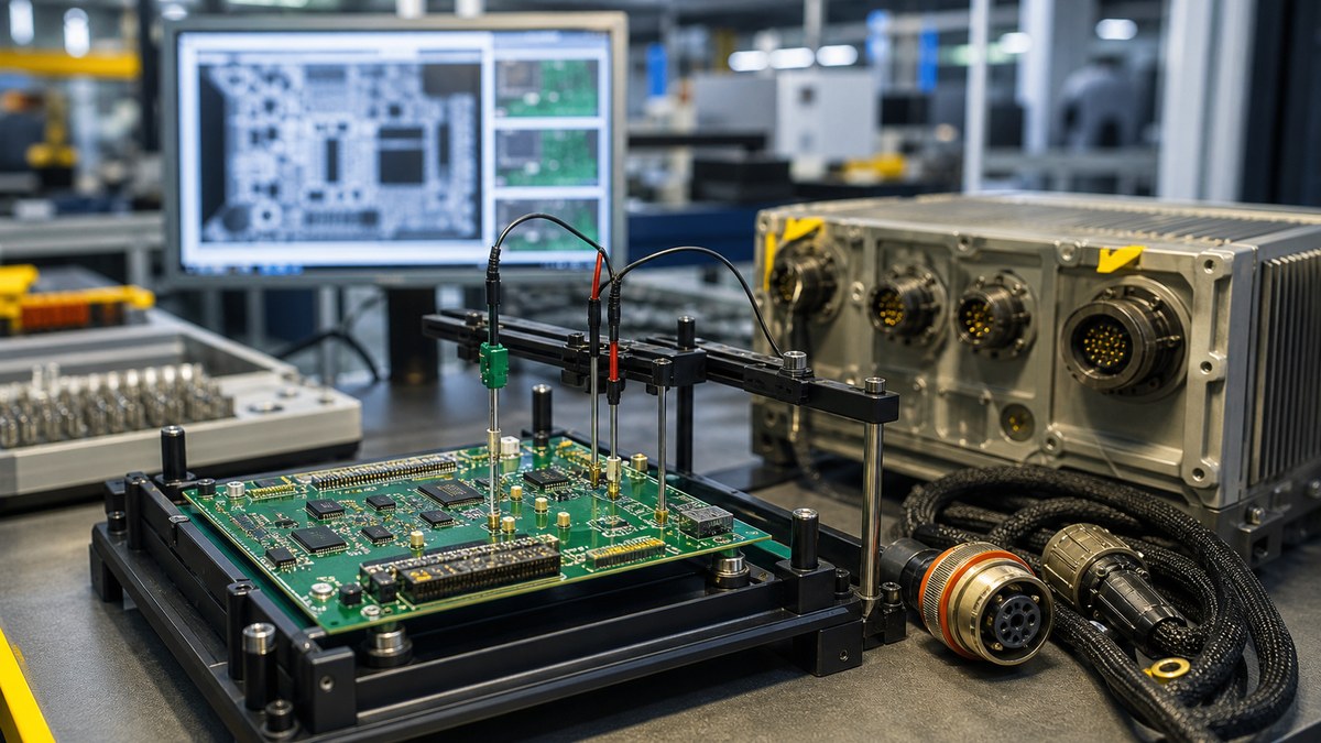
Mining equipment PCB assembly under electrical test with rugged connector harness and sealed enclosure
Testing should be planned before production release, especially when cables, connectors, sealed boxes and field power inputs are involved.

Useful test points should be accessible after assembly, not hidden under large components or blocked by the enclosure. If the board has firmware, define how programming and verification are handled. If the product uses sensors, motors, relays or communication interfaces, list the pass/fail behavior in simple language. A supplier’s PCB test equipment capability should be part of the RFQ discussion when the board needs repeatable inspection instead of only continuity checks.

RFQ checklist for custom PCB design for mining

A useful RFQ package lets the supplier review reliability risks before quoting cost and lead time. Send the same controlled package to every supplier if you want to compare quotes fairly.

  1. Gerber files, drill files, netlist and controlled revision number.
  2. Board drawing with thickness, outline tolerance, mounting holes and connector keepouts.
  3. Stackup, copper weight, material preference and surface finish requirement.
  4. Expected operating voltage, current load, thermal concern and enclosure notes.
  5. BOM, approved substitutes, centroid file and assembly drawing if PCBA is included.
  6. Coating, potting, cleaning, labeling, packaging or box-build requirements.
  7. Test plan with required measurements, programming steps and pass/fail criteria.
  8. Compliance notes for the final equipment, especially if the use environment is regulated.

Supplier questions buyers should ask

The best supplier questions are specific enough to reveal whether the factory has reviewed the board as a mining electronics assembly, not just a generic PCB. Use the questions below before approving production.

  • Which part of this design creates the highest manufacturing risk?
  • Are the mounting holes, edge clearances and connector keepouts suitable for the enclosure?
  • Is the copper weight enough for the stated current and temperature target?
  • Do any components need adhesive, mechanical support or layout changes for vibration?
  • Which components have sourcing risk, and are substitutes already approved?
  • Can the test points still be reached after assembly or box build?
  • What should be changed before moving from prototype to production?

FAQ

What is custom PCB design for mining?

Custom PCB design for mining means designing a circuit board or PCBA for equipment used around mining operations, such as sensors, controllers, lighting, communication modules, power electronics or monitoring devices. The design must consider dust, vibration, moisture, power stress, enclosure fit, connectors, testing and production repeatability.

Does a mining PCB need a special material?

Not always. Many mining control or sensor boards can use FR4 when the electrical load and temperature are moderate. High-current, high-heat, compact or harsh-environment designs may need heavier copper, higher-grade laminate, HDI, metal-backed construction, coating or a different stackup. The material should follow the real design risk.

Can a PCB supplier certify mining equipment?

A PCB supplier can support reliable board fabrication, assembly, traceability, inspection and documentation. Certification for equipment used in regulated mining or hazardous environments is usually a system-level issue. Confirm ATEX, IECEx, MSHA or local requirements with qualified compliance specialists before production decisions.

What files are needed for a mining PCB quote?

Send Gerber files, drill files, board drawing, stackup, copper weight, surface finish, BOM, centroid file, assembly drawing, enclosure notes and test requirements. If the board will be coated, potted or installed in a sealed box, include those details in the first RFQ instead of adding them later.

What causes delays in mining PCB projects?

Common delays include unclear enclosure drawings, missing connector orientation, unapproved component substitutes, vague test criteria, incomplete power requirements and late coating or box-build decisions. A controlled RFQ package helps the supplier check manufacturability before committing to lead time.

Conclusion

Custom PCB design for mining should be treated as a rugged electronics project, not a normal board order with a different label. Start with the environment, enclosure, connectors, power input, heat path, component sourcing and test plan. Then ask the supplier to review the files for manufacturability before quote approval. That process gives the buyer a better chance of receiving a board that can be assembled, inspected and supported in real mining equipment.
You may also like

Custom PCB Design for Industrial Use: Enclosure, Power and I/O Checks
Monday, July 13th, 2026
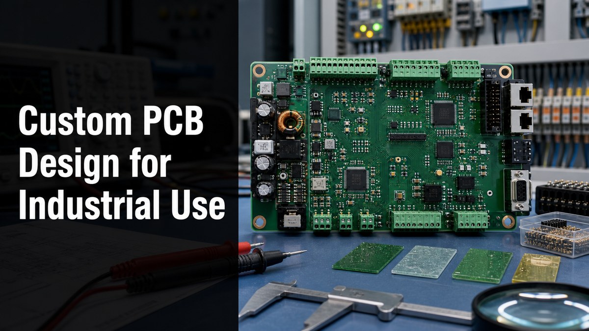
Custom PCB design for industrial use with terminal blocks, power circuitry and test tools

Custom PCB design for industrial use means designing the bare board and assembly around the real installation: enclosure size, field wiring, power noise, vibration, temperature, moisture, service access and test coverage. A board that works on a lab bench can still fail in a cabinet, pump controller, sensor node or factory gateway if the PCB layout ignores connectors, grounding, protection, mounting and production test points.

For an industrial product, the best PCB design brief is not only a schematic and a Gerber file. It should explain the operating voltage range, load current, connector map, enclosure limits, ambient temperature, coating or potting needs, expected service life, and how the board will be tested before shipment. Those details help the PCB manufacturer catch risk before the design moves into fabrication and assembly.

What Is Custom PCB Design for Industrial Use?

Custom PCB design for industrial use is the process of turning an industrial product requirement into a manufacturable board layout that can survive field wiring, power variation, mechanical stress and repeatable production testing. It is different from a generic electronics board because the installation environment becomes part of the design input.

An industrial controller, power monitor or equipment interface often needs larger terminal blocks, screw mounting holes, isolation gaps, surge protection, clear service labels and room for hand tools. The base material may still be a standard FR4 Printed Circuit Board, but the layout rules, copper weight, coating decision and connector placement should be chosen for the real equipment, not for a clean prototype demo.

Start With the Enclosure, Not Only the Circuit

The enclosure fixes many PCB design decisions before trace routing begins. Board outline, mounting holes, connector direction, LED visibility, cable bend radius, airflow and service clearance all depend on the box or cabinet where the board will be installed.

Before layout, confirm the board outline against the mechanical drawing. Check whether connectors must face a panel opening, whether screw terminals need finger access, and whether high-voltage or high-current areas need physical separation from signal wiring. If the board is part of a complete product rather than a loose PCB, coordinate early with the Box Build Assembly plan so cable routing, labels, displays and mechanical fasteners are not solved after the PCB is already finished.

Enclosure factor PCB design check Why it matters
Mounting points Hole size, copper keep-out, washer clearance Prevents cracked solder joints and board flex
Panel connectors Connector height, orientation and access Avoids cable strain and rework during assembly
Airflow Heat source placement and component height Reduces hot spots in sealed or crowded cabinets
Coating or potting Keep-out around connectors, switches and test pads Prevents coating from blocking service points
Service access Readable silkscreen and reachable fuses/test points Helps technicians diagnose the unit in the field

Design the Power Input for Real Factory Conditions

Industrial PCB power design should assume voltage variation, switching noise, inrush current and wiring mistakes instead of assuming a perfect bench supply. The exact protection scheme depends on the product, but the layout should reserve room for protection, filtering and thermal relief.

For DC industrial boards, check reverse-polarity protection, fuse or resettable protection, surge or transient suppression, input filtering, regulator heat, copper width and connector current rating. For boards that switch motors, relays, heaters or solenoids, keep noisy current loops compact and separated from sensors, analog inputs and communication traces. High-current or high-heat industrial applications may need heavier copper, metal-core materials, ceramic substrates or another special PCB structure instead of a basic two-layer FR4 board.

Protect I/O Before It Reaches the MCU

Field I/O is one of the most common weak points in industrial PCB design because long cables carry noise, ESD, surge and wiring errors directly to the board edge. Treat every external connector as a risk entry point.

Place ESD or surge protection close to the connector when required. Keep isolation slots, creepage and clearance appropriate for the voltage category. Put pull-ups, filtering, common-mode chokes or termination near the interface they protect. For RS-485, CAN, Ethernet, sensor inputs or dry-contact I/O, make grounding and shield termination choices early so the PCB layout does not fight the installation wiring later.

Connector selection also affects assembly and sourcing. A design that depends on a rare terminal block or long-lead-time relay may be difficult to build during a shortage. Early Component Sourcing review helps confirm package availability, approved alternates and whether the BOM can support prototype and production builds.

Plan DFM, Assembly and Test Points Together

A good industrial PCB layout is not finished until assembly access and test coverage are planned. If test pads, programming headers and fixture access are added at the end, the board may pass a prototype build but become slow or expensive in production.

Confirm component orientation, panelization, fiducials, solder mask clearance, through-hole access, connector height and coating keep-outs before release. For the assembled product, define which rails, interfaces and functional outputs must be checked. The layout should include accessible test pads for ground, input voltage, main regulators, communication signals and critical sensor lines. A related engineering guide on Circuit Board Test Points can help teams decide which signals deserve fixture access before the first production batch.

If the supplier will handle both PCB fabrication and PCBA, PCB Assembly, SMT, PCB SMT by EBest Circuit (Best Technology), send the assembly drawing, BOM, pick-and-place file, test plan and coating requirements together. Separating fabrication questions from assembly questions often hides problems until parts are already on order.

Industrial PCB Design Checklist Before RFQ

The RFQ package should let the manufacturer review risk, not just quote a board size and layer count. Missing details usually turn into delayed questions, wrong assumptions or rework.

  • Gerber files, drill files, stackup notes and controlled impedance needs if applicable.
  • Board outline with enclosure drawing or DXF when connectors and mounting holes are critical.
  • BOM with manufacturer part numbers, approved alternates and lifecycle notes.
  • Assembly drawing with polarity marks, connector orientation and no-fit parts.
  • Expected environment: temperature, humidity, vibration, dust, splash, coating or potting.
  • Power input range, load current, surge concerns and isolation requirements.
  • Test requirements: programming, in-circuit checks, functional test and inspection points.
  • Packaging and box-build notes if the PCB ships as a complete module.

Common Mistakes That Make Industrial Boards Hard to Build

Most industrial PCB mistakes are not exotic layout errors; they are practical mismatches between the board, the cabinet, the wiring and the production process. Catching them before fabrication saves more time than debugging them after assembly.

Mistake Likely result Better design action
Connectors placed without cable clearance Field wiring bends sharply or blocks the cover Check cable path against enclosure CAD
No test access for power rails Production test becomes slow and manual Add test pads near regulators and protected I/O
Small copper paths for load current Heating, voltage drop or early failure Check copper width, copper weight and thermal relief
Protection parts far from connectors ESD or surge reaches sensitive ICs first Place protection near external entry points
No alternates for industrial connectors Build delay during component shortage Review BOM availability before final layout

Supplier Questions for an Industrial PCB Project

Use supplier questions to check whether the PCB manufacturer understands the product conditions, not only the drawing package. The answers should expose DFM gaps early.

  • Can you review connector clearance against the enclosure drawing?
  • Do any parts in the BOM have long lead time, EOL risk or weak alternates?
  • Which test points are needed for production fixture testing?
  • Should the board use thicker copper, different laminate, coating or selective keep-outs?
  • Can fabrication, assembly, coating and box build be reviewed as one workflow?
  • Which inspection records or test reports will be provided with the finished boards?

FAQ

What files are needed for a custom PCB design for industrial use?

Send Gerber and drill files, BOM, pick-and-place file, assembly drawing, board outline, enclosure drawing if available, test requirements and operating environment notes. For industrial boards, the enclosure, connector map, power range and coating requirements are often as important as the PCB data itself.

Does every industrial PCB need conformal coating?

No. Coating depends on moisture, dust, chemical exposure, voltage spacing and service requirements. If coating is needed, the PCB should include keep-outs around connectors, switches, jumpers, labels and test pads so coating does not block assembly or maintenance.

How should I choose materials for an industrial PCB?

Start with temperature, current, voltage, mechanical load and heat dissipation. FR4 is common for many control boards, but high-current, high-temperature, RF, heavy copper, metal-core or ceramic requirements may call for a different stackup or special PCB process.

Why do industrial PCBs need more test points than simple prototypes?

Production builds need repeatable checks. Test points give fixtures access to voltage rails, programming pins, communication lines and critical I/O. Without them, technicians may rely on slow manual probing or miss faults that only appear after installation.

Final Recommendation

For custom PCB design for industrial use, review the board as part of a field product: enclosure, wiring, power, I/O protection, assembly, sourcing and test coverage. The strongest RFQ package gives the manufacturer enough context to find DFM, BOM and reliability risks before the first boards are built.

You may also like

PCB vs PCBA: Bare Board, Assembly and Sourcing Differences
Thursday, July 9th, 2026

ï»ż

PCB vs PCBA: What Is the Difference?

A PCB is the bare printed circuit board: copper traces, solder mask, pads, vias, holes and surface finish, but no assembled electronic components. A PCBA is the completed assembly after components are mounted and soldered onto the PCB, then inspected and tested. In sourcing terms, PCB usually means bare board fabrication, while PCBA means PCB fabrication plus component procurement, SMT or through-hole assembly, inspection and functional checks.

This PCB vs PCBA guide explains the difference from an engineering and purchasing point of view, so you know what to request, what files to prepare and how each choice affects cost, lead time and quality control.

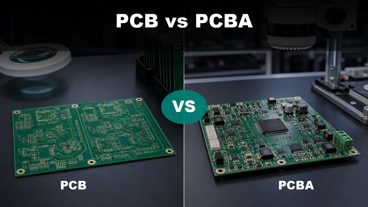
PCB vs PCBA comparison with a bare PCB on the left and assembled PCBA on the right
PCB means the bare board; PCBA means the assembled board with components, solder joints and testing.

What Is a PCB?

A PCB, or printed circuit board, is the physical platform that connects electronic components through copper traces. It may include laminate material, copper layers, solder mask, silkscreen, plated holes, vias, pads, slots and a surface finish such as HASL, ENIG or OSP.

A bare PCB does not perform the final product function by itself. It is the circuit carrier. Before components are added, the factory can inspect board dimensions, copper quality, solder mask registration, hole plating, impedance requirements and electrical continuity. For buyers, a PCB order usually requires Gerber files, drill files, stackup notes and fabrication specifications.

What Is a PCBA?

A PCBA, or printed circuit board assembly, is the PCB after electronic components have been installed and soldered. It may include SMT components, through-hole components, connectors, cables, heat sinks, firmware programming and test records depending on the project scope.

PCBA work is more than placing parts on a board. The supplier must manage component sourcing, stencil setup, solder paste printing, pick-and-place, reflow, through-hole soldering when needed, AOI, X-ray for some packages, cleaning if required, inspection and functional testing. For buyers, a PCBA order usually needs Gerber files, BOM, pick-and-place data, assembly drawings and test requirements.

PCB vs PCBA: The Core Difference

The core difference is assembly status. PCB is the bare board before components; PCBA is the assembled and tested electronic board after components are installed.

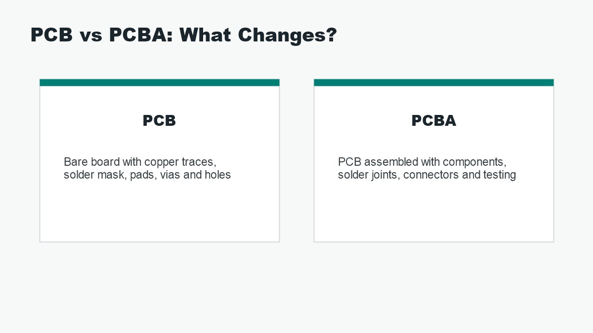
PCB vs PCBA definition graphic explaining bare board and assembled board differences
The move from PCB to PCBA adds component sourcing, assembly, soldering, inspection and testing.
Item PCB PCBA
Meaning Bare printed circuit board Printed circuit board assembly
Components No assembled components Components mounted and soldered
Main factory work Board fabrication Fabrication, sourcing, assembly and test
Files usually needed Gerber, drill, stackup notes Gerber, BOM, pick-and-place, assembly notes, test plan
Quality focus Trace, hole, solder mask, surface finish, electrical test Solder joints, polarity, component value, function and reliability
Best for Board-only fabrication or buyer-managed assembly Turnkey prototypes, samples, validation and production builds

How a PCB Becomes a PCBA

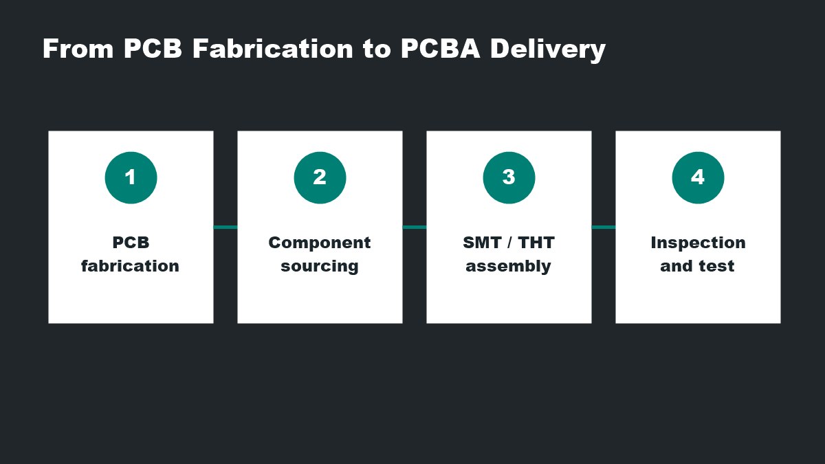
A PCB becomes a PCBA when the bare board moves through component sourcing, solder paste printing, SMT placement, reflow soldering, through-hole assembly when needed, inspection and testing.

Process flow from PCB fabrication to component sourcing, SMT assembly, inspection and PCBA delivery
PCBA delivery adds assembly and test steps after bare PCB fabrication.

For SMT assembly, solder paste is printed through a stencil, components are placed by machine, and the board goes through reflow. Through-hole components may be soldered by wave soldering, selective soldering or manual soldering depending on volume and design. After that, inspection and testing confirm whether the assembled board meets the order requirements.

Which One Should You Order: PCB or PCBA?

Order a PCB when you only need the bare board or when your team will buy components and assemble the boards elsewhere. Order PCBA when you want one supplier to manage the board, parts, assembly and test process.

PCB-only orders make sense when you already have assembly capability, want to control component purchasing, or need bare boards for internal trials. PCBA is usually better when you need working samples, production builds, functional testing, less handoff risk or one quotation that includes more of the manufacturing work.

The wrong scope can waste time. If you request PCB when you really need PCBA, you may receive good bare boards but still have no working units. If you request PCBA without a clean BOM and assembly data, the supplier may need extra clarification before quoting or building.

Cost Difference Between PCB and PCBA

PCB cost is usually driven by board size, layer count, material, copper thickness, surface finish, hole requirements, impedance control, panelization and quantity. PCBA cost adds component cost, sourcing risk, stencil, placement, soldering, inspection, test fixture needs and labor.

For simple boards, the bare PCB may be a small part of the total assembled product cost. For complex assemblies, component availability and testing can matter more than board fabrication price. Buyers should compare quotes by scope, not by headline price. A PCB quote and a PCBA quote are not equivalent unless the included work is the same.

Quality Control: PCB vs PCBA

PCB quality control checks whether the bare board was fabricated correctly. PCBA quality control checks whether the full assembled circuit was built correctly and can work as intended.

For PCB fabrication, common checks include electrical test, visual inspection, hole plating review, solder mask inspection and dimensional checks. For PCBA, the inspection scope may include solder paste quality, component placement, polarity, solder joint quality, AOI, X-ray for hidden joints, ICT or functional testing. The more complete the assembly, the more important test planning becomes.

Files Needed for PCB and PCBA Quotes

PCB and PCBA quotes need different document packages. Sending the right files early helps avoid delays and wrong assumptions.

  • For PCB: Gerber files, drill files, board thickness, copper weight, layer count, material, surface finish, solder mask color and special requirements.
  • For PCBA: PCB files plus BOM, pick-and-place file, assembly drawing, component polarity notes, programming requirements, test plan and packaging requirements.
  • For turnkey PCBA: approved alternates, manufacturer part numbers, substitute rules and critical component notes are especially useful.

Common Buyer Mistakes

Many PCB vs PCBA problems happen because the order scope is unclear. A buyer may ask for a PCB quote while expecting assembled boards, or send a BOM without confirming footprints and polarity.

Before requesting a quote, decide whether you need bare boards, consigned assembly, turnkey PCBA, prototype assembly or mass production. Check that every component in the BOM has a package, value, manufacturer part number when needed and a matching footprint. If the board needs firmware, test points or a fixture, mention that before production starts.

FAQ

Is PCB the same as PCBA?

No. PCB means the bare printed circuit board. PCBA means the printed circuit board assembly after components are mounted, soldered, inspected and tested.

What does PCBA stand for?

PCBA stands for printed circuit board assembly. It refers to a PCB that has been assembled with electronic components and is ready for inspection, testing or product integration.

Can I order PCB fabrication without assembly?

Yes. If you only need bare boards, order PCB fabrication. You will still need a separate assembly plan if the boards must become working electronics.

What files are needed for PCBA?

PCBA usually needs Gerber files, drill files, BOM, pick-and-place data, assembly drawings, polarity notes and test requirements. Turnkey assembly also needs clear component sourcing rules.

Why is PCBA more expensive than PCB?

PCBA includes more work: component sourcing, stencil, SMT or through-hole assembly, soldering, inspection, testing and handling. The components themselves can also cost more than the bare board.

Which is better for prototypes, PCB or PCBA?

If you only want to check board fabrication, PCB is enough. If you need working samples for validation, firmware, testing or customer review, PCBA is usually the right scope.

Does PCBA include functional testing?

Not always. Functional testing must be defined in the order scope. Some PCBA orders include only assembly and visual inspection, while others include ICT, programming or custom functional tests.

Can the same supplier handle PCB and PCBA?

Yes, many suppliers can support both PCB fabrication and PCBA. This can reduce handoff issues, but the buyer still needs to provide complete files, approved components and clear test requirements.

Final Thoughts

The simplest way to remember PCB vs PCBA is this: PCB is the board, PCBA is the assembled electronic board. If you need only fabricated boards, request PCB. If you need working assemblies, request PCBA with BOM, placement data and test requirements.

If you are sourcing PCB fabrication or turnkey PCBA for prototypes, sample builds or production, BestPCBs can help review fabrication details, assembly requirements and quotation scope. Contact the engineering team at sales@bestpcbs.com for technical support and a quote.

You may also like

Assembling Circuit Boards: The Complete PCB & PCBA Guide
Friday, May 8th, 2026

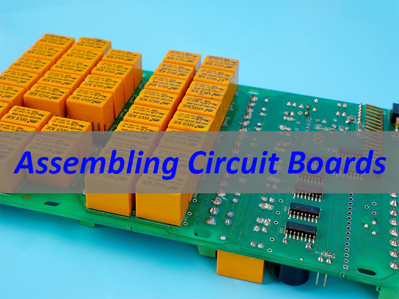
Assembling circuit boards is the step where a design becomes a real, working product. It sounds straightforward. In practice, it involves a precise chain of manufacturing steps — and a single weak link can mean failed boards, delayed launches, or expensive respins.

This guide walks through the full process. We cover what printed circuit board assembly actually involves, how each step works, what materials and finishes to choose, and how to avoid the mistakes that slow most projects down. We also explain what to look for when choosing a circuit board assembly service — and answer the questions engineers ask us most often.

 Assembling Circuit Boards

What Is Assembling Circuit Boards (PCBA)?

Assembling circuit boards — also called printed circuit board assembly, or PCBA — is the process of mounting and soldering electronic components onto a bare PCB. The result is a fully populated board that can be powered on and function inside a product.

However, the process involves more than just placing parts. It also includes solder paste printing, reflow soldering, through-hole insertion, automated inspection, X-ray checks for hidden joints, and functional testing. Each stage must be executed correctly. Because if one step fails, it affects every board in that batch.

It is also worth noting what PCBA does not include. It does not refer to bare PCB fabrication on its own. And it does not refer to chip-level semiconductor manufacturing. PCBA sits between those two — it is the assembly stage that turns fabricated boards and sourced components into working electronics.

PCB vs. PCBA: What Is the Difference?

Engineers sometimes use these terms interchangeably. In reality, they describe two different products at two different stages of manufacturing.

TermWhat It IsWhat It Includes
PCBBare boardCopper traces, vias, pads, solder mask, silkscreen — no components
PCBAAssembled boardPCB with all components soldered on, inspected, and tested
One-Stop ServiceFull turnkeyPCB fabrication + BOM sourcing + SMT/THT assembly + testing, from one vendor

The difference matters when sourcing. If you order a PCB, you still need to find an assembly house separately — and manage the handoff between them. In contrast, a one-stop circuit board assembly service handles fabrication, components, and assembly under one roof. This removes a common source of quality gaps and delays.

The Printed Circuit Board Assembly Process, Step by Step

Understanding the process helps engineers make better design decisions. Here is how a professional manufacturer works through each stage.

Step 1 — Engineering Review and DFM

Before anything is manufactured, the engineering team reviews your Gerber files, BOM, and assembly drawings. They look for issues that would cause problems in production — wrong pad sizes, missing clearances, risky component orientations. This review produces a DFM (Design for Manufacturing) report. Fixing problems at this stage takes hours. Fixing them after production starts takes weeks.

Step 2 — PCB Fabrication

The bare board is manufactured to spec. This means the correct layer stackup, copper weight, drill sizes, surface finish, and impedance control. Boards can range from single-layer to 50+ layers, depending on the circuit design.

Step 3 — Component Sourcing and Incoming Inspection

All parts are procured from authorized distributors or verified suppliers. Before they go into assembly, incoming quality control checks markings, dimensions, and key electrical values. This step is the first line of defense against counterfeit components — a real and growing problem in the electronics supply chain.

Step 4 — Solder Paste Printing

A stencil printer deposits solder paste onto the SMT pads. Too little paste causes cold joints. Too much causes bridging. After printing, automated solder paste inspection (SPI) checks every deposit before the board moves forward.

Step 5 — SMT Pick-and-Place

High-speed machines pick surface mount components — resistors, capacitors, ICs, BGAs, QFNs — and place them precisely on the solder paste. Modern equipment handles parts down to 01005 size (0.4 × 0.2 mm) with placement accuracy of ±0.025 mm.

Step 6 — Reflow Soldering

The populated board passes through a reflow oven. The temperature profile is controlled precisely so the solder paste melts and solidifies correctly. Profile design is especially important for lead-free soldering and for boards with high-Tg substrates.

Step 7 — Through-Hole Assembly

Connectors, transformers, and other through-hole components are inserted next. Soldering is done by wave soldering or selective soldering, depending on the board layout. Selective soldering is preferred when SMT components are nearby and could be damaged by the heat of a full wave pass.

Step 8 — Automated Optical Inspection (AOI)

AOI machines scan every joint and every placed component. They detect missing parts, polarity errors, tombstoning, solder bridges, and insufficient solder. Anything flagged is reviewed before the board continues to testing.

Step 9 — X-Ray Inspection

For BGAs and QFNs, the solder joints are hidden under the component body. AOI cannot see them. X-ray inspection can. This step is essential for high-reliability applications and for any design with area-array packages.

Step 10 — Functional Testing

Finally, each board is powered on and tested against your specification. Depending on volume and requirements, this may use flying probe testing, ICT, or a custom functional test fixture. Only boards that pass leave the facility.

Materials and Surface Finishes for Circuit Board Assembly

The substrate and surface finish you specify affect soldering quality, thermal performance, and shelf life. Here is a practical reference for making those choices.

Substrate Options

MaterialTg (°C)Best For
FR4 Standard (KB 6160, S1141)130–140General commercial electronics
FR4 Mid-Tg (IT 158, S1000H, S1150G)150Industrial, higher-temperature environments
FR4 High-Tg (IT180A, S1000-2M, FR408)170–180Automotive, power electronics, lead-free assembly
High-Speed (M4/M6/M7, TU-872SLK, IT-958)—5G, RF, high-frequency signal integrity
Rogers 4350B / 4003, TMM series—Microwave, antenna, radar
PTFE (Rogers, Taconic, Arlon, Nelco)—Ultra-high frequency, aerospace RF

Surface Finish Options

FinishShelf LifeKey StrengthCommon Use
HASL Lead-Free12 monthsLow cost, robust solderabilityGeneral PCBs, through-hole designs
ENIG12 monthsFlat surface, excellent for BGA and fine-pitchHigh-density SMT assemblies
OSP6 monthsFlat, RoHS-compliant, lowest costHigh-volume SMT production
Immersion Silver6 monthsExcellent solderability, flat surfaceFine-pitch, RF boards
ENEPIG12 monthsWire bonding and soldering compatibleMixed technology, advanced packaging
Hard Gold / Soft Gold24 monthsContact wear resistanceEdge connectors, gold fingers

Tip for prototype builds: If your design includes BGA components, ENIG is the safest choice. It gives you a flat, consistent surface that reduces the risk of wetting failures — which are time-consuming to diagnose during early development.

PCB Manufacturing Capability Reference

Knowing your manufacturer’s process window in advance prevents redesigns. The table below reflects EBest Circuit’s verified production parameters, drawn directly from our current process capability document.

ParameterStandardAdvanced
Layer Count1–50 layersUp to 100L (≄50L requires review)
Board Thickness0.4 – 6 mm0.15 – 10 mm
Min. Laser Drill0.10 mm0.070 mm
Min. Mechanical Drill0.15 mm—
Inner Layer Copper0.5 – 6 ozUp to 20 oz (≄12 oz requires review)
Outer Layer Copper0.5 – 10 ozUp to 28 oz
Min. Line Width/Space — 1 oz inner4 / 4.5 mil3.5 / 3.5 mil
Min. Line Width/Space — 1 oz outer3.5 / 4 mil3 / 3 mil
Min. BGA Pad Diameter10 mil (ENIG: 8 mil)8 mil
Max. Board Size (≄3 layers)580 × 762 mm580 × 1220 mm
Hole Position Tolerance±0.076 mm±0.05 mm
PTH Aspect Ratio12:125:1

For high-frequency designs, EBest Circuit supports Rogers 4350B, Rogers 4003, TMM series, and PTFE-based laminates from Rogers, Taconic, Arlon, and Nelco. Controlled impedance is available with ±10% standard tolerance.

DFM: The Step That Saves the Most Time When Assembling Circuit Boards

Design for Manufacturing (DFM) analysis happens before production starts. Yet it is the step that has the biggest impact on how smoothly the entire assembly process goes.

Here is why. An issue caught at the DFM stage takes a few hours to resolve. The same issue caught after boards have been assembled — or worse, after they have shipped — can require a full respin and weeks of lost time. So while DFM may feel like a delay at the start of a project, it almost always saves time overall.

What a Good DFM Report Covers

  • Pad geometry vs. component footprint â€” mismatches cause tombstoning and cold joints during reflow
  • Component clearance from board edge â€” too little clearance causes damage during depaneling
  • Thermal relief on through-hole pads â€” without it, heavy copper planes prevent proper wave-solder wetting
  • Via-in-pad under BGAs â€” unfilled vias wick solder away and create open joints
  • Component orientation consistency â€” aligning all polarized parts in the same direction reduces placement errors
  • BOM consolidation opportunities â€” reducing unique part count lowers cost and procurement risk
  • Stencil aperture sizing â€” correct aspect ratios ensure proper paste release on fine-pitch pads
  • Test point placement â€” accessible nodes allow flying probe or ICT coverage without special fixturing

How EBest Circuit approaches DFM: Every order includes a formal DFM pre-review report before production begins. Our engineers have 20+ years of PCB and PCBA experience. In addition to the DFM report, we also provide a BOM optimization list — so component cost and availability issues are addressed before any parts are committed.

Printed Circuit Board Assembly Testing Methods

Testing is the final quality gate. The right method depends on your board complexity, order volume, and the reliability level your application requires. In general, more testing costs more per board — but it costs far less than a field failure.

MethodWhat It DetectsBest For
AOIMissing parts, polarity errors, solder bridges, insufficient solderAll assemblies — inline after reflow
X-RayHidden joint quality — BGAs, QFNs, buried viasHigh-density and BGA-heavy boards
ICT (In-Circuit Test)Component values, opens, shorts, basic node functionHigh-volume production with test fixtures
Flying ProbeOpens, shorts, passive values — no fixture neededPrototypes and small batches
Functional Test (FCT)Full board performance against customer specEnd-product verification at all volumes
Burn-InEarly-life failures and infant mortalityMedical, aerospace, defense applications

As a general rule, flying probe combined with functional testing covers most prototype needs without requiring any fixture investment. For volume production, ICT provides higher throughput and lower per-unit cost once the fixture is paid for.

Prototype and Low Volume Circuit Board Assembly

Not every project starts at high volume. In fact, most engineering projects go through several stages before production ramps up — concept verification, design validation, pre-production pilots, and then volume runs. Each stage has different requirements.

For prototype circuit board assembly, speed and flexibility matter more than unit cost. You want to iterate quickly. You also want to catch design issues before they are locked into production tooling. A good assembly partner at this stage provides active DFM feedback, not just a file-and-run service.

For low volume circuit board assembly â€” typically defined as batches from 10 to a few hundred units — the priorities shift slightly. Lead time and consistent quality become more important. Component availability also matters more, because spot-buying small quantities introduces substitution risk that a volume buyer can usually avoid.

There is also a practical reason to use the same manufacturer for both prototype and volume work. When you switch suppliers between stages, the process conditions change — solder paste type, reflow profile, stencil design, inspection thresholds. A board validated on one manufacturer’s process may behave differently on another’s. Continuity removes that variable.

At EBest Circuit: We actively support prototype and small-batch orders. Engineers at the R&D and validation stage are a core part of our customer base — not a lower-priority order type. Our 1.5-week PCBA turnaround applies to prototypes as well as volume runs.

How to Choose Circuit Board Assembly Services?

With many suppliers offering circuit board assembly services, it is easy to focus on price and miss the factors that actually determine whether your project succeeds. Here is what to evaluate before committing to a manufacturer.

Match Technical Capability to Your Design

First, check whether the manufacturer can actually build your board. Get their process capability table and compare it to your design parameters — minimum line width, drill sizes, layer count, impedance requirements, and any specialty materials. A supplier who cannot hit your specs is not an option, regardless of price.

Look at Quality Certifications

Certifications indicate what kind of manufacturing discipline a company operates under. ISO 9001 is the baseline for general quality management. Beyond that, ISO 13485 covers medical devices, IATF 16949 covers automotive, and AS9100D covers aerospace. These require documented processes, traceability systems, and regular third-party audits — which is exactly what you want in a supplier.

Evaluate Engineering Support

There is a significant difference between a manufacturer who reviews your files before production and one who simply runs whatever you submit. For engineers developing new products, active DFM feedback, BOM optimization input, and process adaptation guidance are worth far more than a marginally lower board price. Problems found before production cost hours. The same problems found after assembly cost weeks.

Ask About Component Sourcing

Counterfeit components are a genuine risk. Ask directly: where do parts come from? Are they sourced from authorized distributors? What does incoming inspection involve? A supplier who cannot answer these questions clearly is a supplier whose component quality you cannot verify.

Check Traceability Systems

For regulated industries — and for any complex product where field failures are serious — traceability matters. Can the manufacturer tell you, after shipment, which component batch was used on a specific board? If they rely on paper records or manual logs, that question may take days to answer. If they use a digital MES, it should take seconds.

Why Engineers Choose EBest Circuit?

EBest Circuit (Best Technology) has specialized in PCB and PCBA manufacturing for over 20 years. In that time, we have served more than 10,000 engineers and 1,800+ customers across industrial, medical, automotive, consumer, and aerospace applications. Here is what makes our approach different in practice.

One Account Manager + Three Engineers per Order

Every project is assigned a dedicated account manager and a three-person engineering team covering process, quality, and DFM. When you have a technical question, you get a response from an engineer with relevant experience. You do not get passed to a general support queue.

DFM Report + BOM Optimization List — Included with Every Order

Before production starts, we deliver a written DFM report with specific, actionable findings. We also provide a BOM optimization list that identifies consolidation opportunities and flags components with availability risk. This service is included as standard, not sold separately.

One-Stop: PCB + Components + PCBA

We operate our own PCB factory and our own PCBA factory. In addition, we work with 1,000+ supply chain partners for component sourcing. As a result, you submit one set of files and receive tested, functional boards — without coordinating between separate fabrication and assembly vendors.

1.5-Week PCBA Turnaround

From Gerber files to shipped, tested boards: as fast as 1.5 weeks. That covers the full cycle — PCB fabrication, component procurement, SMT assembly, inspection, and functional testing. This turnaround applies to prototype orders as well as volume runs.

Full Certification Stack

We hold ISO 9001, ISO 13485, IATF 16949, and AS9100D. This means we are qualified to manufacture for medical, automotive, and aerospace applications — with the documentation and traceability those industries require.

5-Second Material and Batch Traceability

Our digital manufacturing system tracks every component lot and every production batch in real time. Any board can be traced from incoming inspection to shipment — and that trace is retrievable in under five seconds.

To get a quote or discuss your project, contact our engineering team at sales@bestpcbs.com. Send your Gerber files and BOM. We will return a DFM report and a quote within 24 hours.

FAQs About Assembling Circuit Boards

What is printed circuit board assembly?

Printed circuit board assembly (PCBA) is the process of soldering electronic components onto a bare PCB to produce a functional electronic board. It includes solder paste printing, SMT pick-and-place, reflow soldering, through-hole assembly, AOI and X-ray inspection, and functional testing. The finished PCBA can be powered on and integrated directly into a product.

What is the difference between PCB and PCBA?

A PCB is the bare substrate — copper traces, vias, pads, and solder mask, but no components. A PCBA has all components soldered on and has passed inspection and testing. In short, a PCB cannot function on its own. A PCBA can.

How long does circuit board assembly take?

EBest Circuit delivers complete PCBA — covering PCB fabrication, component sourcing, SMT assembly, and functional testing — in as fast as 1.5 weeks. Boards with more complex designs or long-lead components may require additional time. We confirm the expected delivery date at the quoting stage.

What certifications should a PCBA manufacturer have?

ISO 9001 covers general quality management and is the baseline to look for. Beyond that: ISO 13485 for medical devices, IATF 16949 for automotive, and AS9100D for aerospace. EBest Circuit holds all four, which means we can support high-reliability applications across all major industries.

What files do I need for a PCBA quote?

The standard set is: Gerber files, a BOM with manufacturer part numbers and quantities, and a pick-and-place centroid file. An assembly drawing in PDF format is helpful but not always required. Send your files to sales@bestpcbs.com and we will respond with a DFM review and quote within 24 hours.

Do you support SMT and through-hole components on the same board?

Yes. We handle mixed-technology boards with both surface mount and through-hole components. Through-hole soldering is performed by wave soldering or selective soldering, depending on the board layout and proximity to SMT parts.

Can I use the same manufacturer for prototype and volume production?

Yes — and we recommend it. Switching manufacturers between prototype and production changes the process conditions your design was validated against. That is a common and often overlooked cause of unexpected failures. EBest Circuit supports prototype, small batch, and full production from the same facility, so process continuity is maintained from first article through volume shipments.

You may also like

What is the Meaning of PCBA? PCBA Process
Tuesday, April 8th, 2025

What Does the PCBA Stand For?

PCBA stands for Printed Circuit Board Assembly.

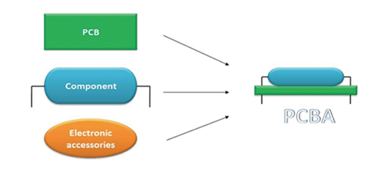
It’s a complete board where all parts are mounted and ready to work. The bare board itself is called a PCB. But once components like resistors, capacitors, and chips are soldered onto it, it becomes a PCBA. Sometimes, some electronic accessories will be soldered onto the PCB surface as well.

What is the Meaning of PCBA? PCBA Process

Key Components in PCBA

The value of a PCBA comes from the components it carries. Each part plays a role in how the circuit works. Let’s go over some of the most common parts:

  • Resistors: Control the flow of current.
  • Capacitors: Store and release energy when needed.
  • Inductors: Manage signals, especially in filters.
  • Diodes: Let current flow in one direction only.
  • Transistors: Switch or amplify signals.
  • ICs (Integrated Circuits): Small chips with many tiny parts inside. They perform complex functions.
  • Connectors: Help connect the board with other systems.
  • Transformers: Change voltage levels for safer or better operation.
What is the Meaning of PCBA? PCBA Process

All these parts must be carefully chosen and placed. A small mistake can stop the board from working right. That’s why design and assembly matter so much.

Types of PCBA Assembly Techniques

1. Surface Mount Technology (SMT)

This is the most common method today. Components are placed directly on the surface of the board. Pick and place machines handle most of the work, which keeps it fast and accurate. SMT supports miniaturized parts and high-speed production.

2. Through-Hole Technology (THT)

This technique uses components with leads that go through holes in the PCB. These leads are soldered on the other side. THT is strong and used for large or high-stress parts like connectors or transformers.

3. Mixed Technology Assembly

Some boards use both SMT and THT. Surface-mount parts go on first, then through-hole components are added by manually. This mix allows for flexible, compact, and reliable designs.

What is the difference in PCB and PCBA?

Though the terms PCB and PCBA are often used together, they describe very different stages in the electronics manufacturing process. And you must to know: PCB are one of important part of PCBA, but PCBA not. Below we listing the key differences between them:

FactorPCBPCBA
StageBlank boardAssembled with components
ComponentsNoYES
FunctionalityNon-functionalFully operational
Manufacturing CostLowHigher (because include the components cost)
TestingBasic inspectionComplete electrical testing
Assembly TechniquesNot applicableSMT, THT, or hybrid
Files NeededGerber, drill filesGerber, BOM, pick & place, assembly files
Lead Time (under same design)ShortRelated longer than PCB

What Is the Use of PCBA?

PCBAs are used in almost everything you see around:

  • Phones: Control your screen, camera, and sound.
  • Computers: Process data, run programs.
  • Vehicles: Support GPS, safety features, engine control.
  • Medical devices: Power equipment like MRI or ECG machines.
  • Home appliances: From smart TVs to microwave ovens.

Without a PCBA, none of these would work. It’s like the brain of any electronic device. From simple tools to high-end gadgets, PCBA plays a big role.

How to Do PCBA Testing?

Testing makes sure the board works as expected. It helps catch issues before the board goes into the final product. There are several ways to test a PCBA:

1. Visual Inspection

This is the first step. Technicians or machines check if parts are in the right place. They also look for bad solder joints, cracks, or missing items.

2. Automated Optical Inspection (AOI)

AOI mainly uses a camera system scans the board. It checks for incorrect or misaligned parts. It’s faster than manual inspection and works well for large batches.

3. In-Circuit Testing (ICT)

ICT checks each component directly. It makes sure resistors, capacitors, and connections work properly.

4. Functional Testing

This test powers the board and simulates how it will be used. It checks whether the PCBA can perform the expected tasks.

5. X-Ray Inspection

Used when components are hard to see, like BGAs (Ball Grid Arrays). The X-ray looks through the board to catch hidden problems.

6. Flying Probe Test

For small batches, probes test different points without a custom fixture. It’s flexible and cost-effective.

7. Testing with jig

This is used for mass production, jig tools are made according to the design files, so it is a customized. Jig testing can save much time compared with flying probe.

EBest Circuit (Best Technology) deeply know the importance of the product quality, so we pay more attention to the PCB board quality checking process. We set a QC department according to ISO9001:2015 and ensure all processes are compliance with quality system.

How Do You Clean a PCBA?

During the PCB assembly process, cleaning a PCBA is an important step, especially after soldering. Residual flux, dust, or moisture can affect the performance of the board. Nowadays, the common cleaning methods used in EBest Circuit (Best Technology) are:

1. Manual Cleaning

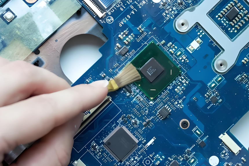
This is the most basic method. A technician uses a soft anti-static brush and high-purity isopropyl alcohol to remove visible flux or dirt. It’s ideal for prototypes, small batches, or after rework or repair. Manual cleaning gives the operator control, especially in tight or delicate areas. However, it’s time-consuming and not suitable for large-scale production.

What is the Meaning of PCBA? PCBA Process

2. Ultrasonic Cleaning

Ultrasonic cleaning is widely used for complex boards and mass production. The PCBA is submerged in a tank filled with a cleaning solution. High-frequency sound waves pass through the liquid, creating microscopic bubbles. These bubbles collapse rapidly, producing a scrubbing action known as cavitation.

This technique reaches tiny gaps under components where brushes can’t go. It’s very effective for removing dried flux, fine dust, or ionic contamination. The process is gentle on components but powerful enough to clean even the most compact assemblies. After cleaning, the board is rinsed and dried with warm air or placed in a drying chamber.

What is the Meaning of PCBA? PCBA Process

3. Dry Ice Cleaning

Dry ice cleaning is a newer, eco-friendly technique. It uses solid CO₂ pellets, also called dry ice, blasted at high speed onto the PCBA surface. As the pellets hit, they turn into gas instantly. This process lifts off dirt, flux, and even adhesives without leaving moisture or residue behind.

What is the Meaning of PCBA? PCBA Process

Dry ice cleaning works well for delicate electronics and is especially useful in industries where cleanliness must meet strict standards. To give customer a highest quality of the PCBA, our SMT factory equipped with the dry ice cleaning machine to ensure a clear surface while improve the efficiency.

PCBA Assembly Process

The PCBA assembly process is relatively simple than PCB manufacturing, actually the most tedious step is to load all the components on the pick and place machine, and set the program parameters. Here we break down all the processes of the mass production PCB assembly, from the solder paste printing to function testing.

1. Solder Paste Printing

First, solder paste is applied to the bare PCB. This paste is mainly consists of silver and tin, a mix of tiny solder particles and flux. A stencil is placed over the board, and the paste is spread across it using a squeegee. The paste sticks only to the exposed pads where components will be mounted.

2. Load components feeder

Load all the components in the feeder of the pick and place machines, make sure all the parameter of components are correct, and double check the direction of chips. It is a simple but tedious step and need much time to check everything is okay. 

2. Pick and Place

After applying solder paste, automated pick-and-place machines begin placing surface-mount components onto the board. These machines work fast and accurately. They follow a file created during PCB design that tells them the exact location for each part. The components sit on the solder paste, which holds them in place temporarily.

3. Reflow Soldering

Next, the assembled board goes through a reflow oven. The oven slowly heats the board in stages. When it reaches a high enough temperature, the solder paste melts and forms strong electrical and mechanical connections between the parts and the board. After this, the board cools down, and the solder solidifies.

This step is only for SMT components. If the board has only through-hole parts, this step may be skipped.

4. Inspection (AOI and Visual)

Once the soldering is done, the board goes through inspection. Automatic Optical Inspection (AOI) machines scan the board using high-resolution cameras. They check for misaligned parts, soldering problems, or missing components. For small production or sensitive areas, manual inspection is also performed to catch anything machines might miss.

5. Through-Hole Component Insertion (If Needed)

If the board uses through-hole technology (THT), this is when those parts are added. Workers or machines insert the components into the holes, and the leads go through to the other side of the board. These components are often bulkier, like connectors or transformers.

6. Wave Soldering (For THT)

For boards with many through-hole parts, wave soldering is used. The board passes over a wave of molten solder that touches the underside. This solders all the leads at once. It’s fast and effective, especially for high-volume production. For small-scale or sensitive boards, hand soldering might be used instead.

7. Final Inspection and Quality Control

After soldering, the entire board is checked again. Technicians or AOI machines inspect the final assembly. They look for cold joints, excess solder, or misplaced parts. Boards may also be tested with X-ray machines to inspect solder joints under BGAs or hidden areas.

8. Functional Testing (FCT)

The next step is functional testing. The board is powered up and tested to make sure it works correctly. This could include checking voltages, signals, response times, and communication with other devices. Engineers may use test jigs or test programs based on the end application.

9. Cleaning (If Needed)

After all soldering and testing, the board might be cleaned to remove flux residue. Depending on the flux used, this could be manual, ultrasonic, or dry ice cleaning. Clean boards are especially important in high-reliability fields like aerospace, automotive, or medical.

10. Conformal Coating or Protection (Optional)

For some applications, a conformal coating is applied. This is a protective layer that shields the board from moisture, dust, and chemicals. It’s often used in harsh environments. Coating can be applied by spraying, dipping, or brushing.

11. Packaging and Shipping

Finally, once the PCBA passes all checks, it’s packed carefully. Anti-static bags, foam, and trays protect it during transport. Labels are added for tracking and traceability. From here, it’s ready to be installed into the final product. Here is a whole process of pcb assembly in EBest Circuit (Best Technology).

PCBA HS Code

Every product for trade needs a code. The HS code for PCBA usually is 8517799000

But depending on the use or market, some customs may use a different classification. For example:

853400 for bare board parts, sometimes be used on certain assembled parts.

847330 for boards used in computers.

853710 for board which used as controller or controller unit.

Noted: Always check with your country’s customs for the right code. Using the wrong one may cause delays or extra costs.

Our PCBA Services

At EBest Circuit (Best Technology), we specialize in end-to-end PCBA services. From design to delivery, we support your project with speed, quality, and reliability. We can be your first choice because:

  1. We have 18+ years in PCB industry
  2. One-Stop Service: PCB fabrication, parts sourcing, SMT/THT assembly, testing
  3. Custom Solutions: From prototypes to mass production, no MOQ
  4. Skilled Engineers: For DFM & DFA checks and process optimization
  5. Strict Quality Control: 9-times QC check, including AOI, X-ray, ICT, and functional testing
  6. Global Delivery: Fast and on time, wherever you are
  7. Component Sourcing: Only original, trusted parts, we have cooperated with digikey, findchips, mouser for over 10 years, and we can get the most competitive price from them.
  8. PCB Fabrication: Rigid, flex, metal-core, ceramic, and more.

Whether you’re working on a simple control board or a multi-layer high-speed system, we’re here to support you.

You may also like

PCB Assembly Manufacturer, Quality-Focused PCBA Service
Tuesday, March 18th, 2025

PCB Assembly plays a crucial role in modern electronics, turning bare circuit boards into functional devices. Without proper assembly, even the most advanced PCB designs cannot perform as expected. Whether for consumer electronics, automotive applications, or aerospace systems, high-quality PCBA ensures reliability and performance. In this guide, we explore everything about PCB assembly, from types and materials to design considerations and industry applications. By the end, you’ll understand why EBest Circuit (Best Technology) is the right partner for your PCB assembly needs.

At EBest Circuit (Best Technology), we specialize in precision-driven PCB assembly services, offering turnkey PCBA solutions, rigorous quality control, and advanced manufacturing capabilities to meet diverse industry needs. With over 18 years of experience, EBest Circuit (Best Technology) provide cost-effective, high-accuracy printed circuit board assembly solutions tailored to your requirements. Feel free to contact us at sales@bestpcbs.com for any doubts or queries you might have.

PCB Assembly Manufacturer, Quality-Focused PCBA Service

What is a PCB Assembly?

PCB assembly (PCBA) is the process of placing and soldering electronic components onto a printed circuit board (PCB) to create a functional electronic device. The assembly process involves multiple steps, including surface-mount technology (SMT), through-hole technology (THT), soldering, and quality inspections. Unlike a bare PCB, a fully assembled PCB has all the necessary components installed, making it ready for integration into electronic systems.

What Are the Different Types of PCB Assembly?

1. Surface-Mount Technology (SMT) Assembly – The most common assembly method, SMT involves mounting components directly onto the surface of the PCB. It allows for smaller, more compact designs and is ideal for high-density applications.
2. Through-Hole Technology (THT) Assembly – THT involves inserting component leads into pre-drilled holes on the PCB and soldering them in place. It provides strong mechanical connections and is used in applications requiring durability.
3. Mixed Assembly – A combination of SMT and THT, mixed assembly is used when a design requires both surface-mounted and through-hole components.
4. Single-Sided & Double-Sided Assembly – Single-sided assembly involves placing components on one side of the PCB, while double-sided assembly places components on both sides, maximizing space and functionality.
5. Box Build Assembly – This type of assembly goes beyond the PCB level, including wire harnesses, enclosures, and full system integration.
6. Turnkey PCB Assembly – A complete service where the manufacturer handles everything from PCB fabrication to component sourcing, assembly, and testing, providing a ready-to-use product.
7. Prototype PCB Assembly – Used for product development and testing before full-scale production.

PCB Assembly Manufacturer

What Materials Are Used to Make PCB Assembly?

Several materials are used in PCB assembly to ensure reliability and performance:

  • PCB Substrate – The base material of the PCB, commonly made from FR4 (fiberglass epoxy), metal core, or ceramic for high-performance applications.
  • Copper Traces – Thin layers of copper form the conductive pathways for electrical signals.
  • Solder Mask – A protective layer applied over copper traces to prevent oxidation and short circuits.
  • Silkscreen Layer – Used for labeling component positions and reference markings.
  • Solder Paste – A mixture of flux and metal alloy used in SMT assembly to attach components before reflow soldering.
  • Electronic Components – Resistors, capacitors, ICs, diodes, and other essential parts that enable the PCB to function.
  • Solder Wire & Flux – Used in THT assembly to create strong electrical connections between components and the PCB.

How to Design PCB Assembly?

  • Component Placement – Arrange components efficiently to optimize space, signal integrity, and heat dissipation.
  • Layer Stack-Up – Define the number of PCB layers to meet electrical and mechanical requirements.
  • Trace Routing – Ensure proper trace width, spacing, and routing strategies to minimize signal interference.
  • Power & Ground Planes – Design stable power distribution and ground layers for noise reduction.
  • Thermal Management – Use thermal vias, heat sinks, and copper pours to manage heat dissipation.
  • DFM (Design for Manufacturability) – Optimize the PCB layout for efficient assembly, reducing potential defects and rework.
  • DFT (Design for Testing) – Include test points and accessibility for automated testing.
  • Bill of Materials (BOM) Creation – List all required components, their specifications, and sourcing details.
Quality-Focused PCBA Service

What Are the Benefits of PCB Assembly?

  • Compact Design – Enables smaller, lightweight devices with high functionality.
  • Cost-Effective Production – Automated assembly reduces labor costs and increases efficiency.
  • High Reliability – Advanced soldering techniques and quality checks ensure long-lasting performance.
  • Scalability – Suitable for both low-volume prototypes and high-volume manufacturing.
  • Customization – Supports specialized requirements, such as high-speed, high-frequency, or high-temperature applications.

What Are the Applications of PCB Assembly?

  • Consumer Electronics – Smartphones, tablets, laptops, and wearable devices.
  • Automotive – Engine control units, infotainment systems, and safety sensors.
  • Medical Devices – Patient monitoring systems, diagnostic tools, and imaging equipment.
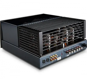
  • Aerospace & Defense – Avionics, communication systems, and radar technology.
  • Industrial Automation – Robotics, control systems, and power electronics.
  • Telecommunications – Networking equipment, signal processing, and wireless communication devices.

Why Choose EBest Circuit (Best Technology) as Your PCB Assembly Manufacturer?

  • Experience & Expertise – Over 18 years of experience in PCB manufacturing and PCB assembly. EBest Circuit (Best Technology) is a leading PCB Assembly Manufacturer, providing manufacturing and sale service of various types of printed circuit boards and quality-focused PCBA Service.
  • Comprehensive Services – Full turnkey, partial turnkey, and consignment assembly options. We provide one-stop service, including PCB assembly and component purchasing and all-around technical support before and after-sales.
  • Quality Assurance – Stringent IPC and industry-standard testing, including AOI, X-ray, and functional testing. The pursuit of quality and innovation is the driving force of EBest Circuit (Best Technology). Every stage, from sourcing raw materials to production, inspection, packaging, and even sales and marketing, strictly follows ISO quality standards to ensure consistency and reliability.
  • Reliable Component Sourcing – Direct partnerships with trusted suppliers to prevent counterfeit parts. We procure all components exclusively from manufacturers or trusted distributors like Digikey, Mouser, Future, TTI, Avnet, and Arrow, ensuring authenticity.
  • State-of-the-Art Equipment – Advanced assembly machines ensure precision and efficiency. By leveraging cutting-edge technology and advanced PCB assembly equipment, we constantly refine our manufacturing processes, enhance testing and measurement techniques, and optimize our quality management system.
  • On-Time Delivery – Expedited services available for urgent orders. No matter where you are, we guarantee on-time delivery for every order.
  • Competitive Pricing – Cost-effective solutions without compromising quality.
  • Customer Support – Dedicated one-on-one sales assistance for a smooth collaboration. With exceptional team, EBest Circuit (Best Technology) ensures prompt responses within 12 hours.

In conclusion, choosing the right PCB assembly manufacturer ensures product reliability, cost-effectiveness, and timely delivery. EBest Circuit (Best Technology) offers expert solutions for various industries with a focus on quality and efficiency. Whether you need a simple prototype or a high-volume production run, our team is ready to support your project. Just feel free to reach out to us at sales@bestpcbs.com to discuss your PCB assembly needs!

 PCB Assembly Manufacturer

FAQs of PCB Assembly

1. What is the difference between PCB and PCB assembly?

  • A PCB (Printed Circuit Board) is the bare board with copper traces, while a PCB Assembly (PCBA) includes all the necessary electronic components soldered onto the board, making it a fully functional unit ready for use.

2. What is the purpose of a pick and place drawing in the SMT process?

  • A pick and place drawing provides detailed guidance for automated SMT machines, specifying component placement, orientation, and reference designators on the PCB. It ensures accurate positioning (including polarity indicators for diodes and capacitors) and facilitates post-assembly inspection.

3. What are counterbores and countersinks?

  • Counterbore: A cylindrical recess with a flat bottom, designed to allow a screw head to sit flush with the PCB surface. Commonly used with flat-head screws to ensure secure mounting, such as for attaching heatsinks or connectors.
  • Countersink: A conical recess that matches the angle of a tapered screw head, such as self-tapping screws. Helps create a smooth, low-profile surface, often used when securing PCBs within enclosures.

The key difference is that counterbore provides a level surface by embedding the screw head within the material. Countersink features a tapered design that aligns the screw and evenly distributes stress.

4. How to distinguish the PTH & NPTH?

  • PTH is PLATING Through Hole, it has copper in the holes inside, which can be conductive.  NPTH is Non PLATING Through Hole, which don’t have copper inside the holes. Through holes means through the top and bottom on the PCB, it could be PTH and NPTH.

You may also like

Special PCB Design, Prototype, Special PCB Manufacturer
Tuesday, March 18th, 2025

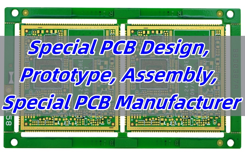
Special PCB is a customized circuit board designed for unique applications where standard PCBs do not meet the required performance, durability, or environmental conditions. These PCBs are used in industries such as aerospace, medical, telecommunications, and automotive, where factors like heat dissipation, high frequency, and miniaturization are crucial. Whether it’s a high-speed PCB, HDI PCB, or heavy copper PCB, each type serves a specific purpose to enhance electronic performance.

EBest Circuit (Best Technology) excel in providing customer-centric support in PCB industry. The team offers special PCB design optimization, material selection guidance, and manufacturing feasibility analysis to the customers. Whether you need a special PCB prototype or full-scale special PCB manufacturing, just feel free to reach out to us at sales@bestpcbs.com, we work closely with you to meet your exact specifications.

Special PCB Design, Prototype, Assembly, Special PCB Manufacturer

What is Special PCB?

A special PCB is a customized printed circuit board that differs from standard PCBs in design, materials, or functionality. It is engineered to meet specific requirements such as high power handling, extreme temperatures, or unique form factors. These boards ensure stability, reliability, and efficiency in demanding applications.

What Are the Different Types of Special PCBs?

Special PCBs can be classified into three main categories based on their materials, functionality, and structure.

1) Material-Based Special PCBs

These PCBs are defined by the materials used to enhance their performance under specific conditions.

Heavy Copper PCB – Uses thick copper layers (≄3 oz) for high current applications and improved thermal management.

Special PCB Design

High Tg PCB – Made with high glass transition temperature (Tg) materials to withstand extreme heat and mechanical stress.

2) Function-Based Special PCBs

This category includes PCBs designed for specific electrical or performance characteristics.

High-Speed PCB – Designed with low-loss materials and controlled impedance for fast signal transmission in networking and computing.

Impedance Control PCB – Maintains precise impedance levels for RF, microwave, and high-frequency circuits.

RF Board – Uses low-loss materials to minimize signal interference in wireless communication, radar, and satellite applications.

Bus Bar PCB – Incorporates embedded copper bars for high current carrying capacity in power distribution systems.

3) Structure-Based Special PCBs

These PCBs are categorized based on their physical design and layout innovations.

HDI PCB – Features microvias, fine traces, and multiple layers for compact, high-density applications like smartphones and laptops.

Extra Thin PCB – Ultra-thin boards designed for compact and flexible electronic devices.

Special PCB Prototype

IC Substrate – Specialized interconnects used to bridge semiconductor chips with larger PCB assemblies.

What Materials Are Used to Make Special PCBs?

The choice of materials in special PCBs determines their electrical performance, heat resistance, and mechanical durability. Here are the key materials used:

1) FR-4

A fiberglass-reinforced epoxy laminate that offers a balance of cost, durability, and electrical insulation. It is commonly used in High Tg PCBs, HDI PCBs, and Impedance Control PCBs where thermal resistance and signal integrity are crucial.

2) High-Tg FR-4

An advanced version of FR-4 with a higher glass transition temperature (Tg), making it suitable for High Tg PCBs and High-Speed PCBs that operate under extreme thermal conditions.

Special PCB Assembly

3) Polyimide

This material provides exceptional thermal stability and flexibility. It is widely used in Extra Thin PCBs and HDI PCBs, where space-saving and durability under heat are essential.

4) PTFE (Teflon)

A low-loss, high-frequency material that is ideal for RF Boards and High-Speed PCBs. Its excellent dielectric properties help maintain signal integrity in wireless and microwave applications.

5) Copper

  • Heavy Copper PCB – Uses thick copper layers (≄3 oz) to support high current loads and enhance heat dissipation.
  • Bus Bar PCB – Features embedded copper bars for efficient power distribution in industrial and automotive applications.

6) BT (Bismaleimide Triazine) Epoxy Resin

This material is used in IC Substrates for its excellent electrical insulation, high-temperature resistance, and mechanical strength. It ensures reliable connections in semiconductor packaging.

7) Low-Dk (Low Dielectric Constant) and Low-Df (Low Dissipation Factor) Materials

These are specialized dielectric materials used in Impedance Control PCBs and High-Speed PCBs to reduce signal loss and maintain consistent impedance for high-frequency applications.

How to Design a Special PCB?

1) Define Requirements

Start by determining the electrical, thermal, and mechanical specifications needed for the application.

2) Select Materials

Choose the right substrate, copper thickness, and surface finish based on operating conditions and performance needs.

3) Create a Schematic

Develop a circuit diagram to define component placement and electrical connections.

4) Layout Design

Optimize routing, layer stack-up, and impedance matching to ensure signal integrity and manufacturability.

5) Prototyping & Testing

Before mass production, test a prototype to validate functionality, thermal management, and reliability.

What Are the Benefits of a Special PCB?

1) High Performance

Custom designs ensure superior electrical and thermal efficiency.

2) Enhanced Durability

Robust materials and specialized coatings increase lifespan, even in harsh environments.

3) Miniaturization

Advanced designs, such as HDI and extra thin PCBs, enable compact, lightweight devices.

4) Reduced Signal Loss

Impedance control and RF materials enhance signal integrity, crucial for high-speed and wireless applications.

What Are the Applications of Special PCBs?

1) Aerospace & Defense

Used in satellite systems, avionics, and military-grade electronics that require reliability under extreme conditions.

2) Automotive Electronics

Essential for EV power systems, engine control units, and ADAS (Advanced Driver Assistance Systems).

3) Medical Devices

Supports high-precision diagnostic equipment, wearable health monitors, and implantable devices.

4) Telecommunications

Used in 5G infrastructure, networking hardware, and high-speed data transmission systems.

Special PCB Manufacturer

Why Choose EBest Circuit (Best Technology) as Your Special PCB Manufacturer?

1) Industry Expertise

With 18 years of experience, EBest Circuit (Best Technology) specializes in manufacturing high-quality special PCBs tailored to unique requirements.

2) Multi-Variety PCB Manufacturing

Electronics manufacturers often require diverse PCB types within a single project. EBest Circuit (Best Technology) offers a wide range of special PCBs, including Heavy Copper, Bus Bar, High-Speed, IC Substrate, Impedance Control, Extra Thin, High Tg, HDI, and RF Boards. Our ability to handle multiple PCB types under one roof simplifies the supply chain, reduces lead times, and ensures consistency across different PCB designs.

3) High Quality

Each special PCB undergoes rigorous testing to meet international quality and reliability standards.

4) Custom Solutions

As a leading special PCB manufacturer, we offer complete customization based on your project needs from special PCB design to special PCB assembly. Not only provide top quality requirements of Special Printed circuit Board and PCBA service for the market but also meet customer special customized requests.

Small-Batch Production

At EBest Circuit (Best Technology), we specialize in low-volume special PCB manufacturing, ensuring that even small orders receive the same level of precision and quality as mass production. This allows customers to test new designs, reduce risks, and accelerate product development.

FAQs Of Special PCB

1. What is the maximum operating temperature for PCBs?
Typically, the working temperature for standard PCB materials is 105-130°C. For high-temperature materials, such as those made with 7316D, the working temperature can reach 150-170°C. However, this material requires a higher MOQ.
2. Is the smallest copper trace width you can do 4mil?
Yes.
3. What PCB material brands do you use?
We use brands like Shengyi, KB, ITTEQ, GDM, and etc.
4. What is the maximum board size you can produce?
The maximum size we can produce is 610mm x 610mm.
5. What is the maximum copper thickness for a PCB?
We can produce a maximum copper thickness of 30oz (1050um).

In conclusion, special PCBs are essential for high-performance, reliable, and efficient electronic applications. Whether you need heavy copper PCBs for power applications or HDI boards for miniaturized devices, selecting the right manufacturer is crucial. EBest Circuit (Best Technology) provides industry-leading expertise, top-notch quality, and tailored solutions to ensure your project’s success. Pls feel free to contact us at sales@bestpcbs.com to get started on your special PCB requirements!

You may also like

FR4 PCB Design, Prototype, Assembly, FR4 PCB Manufacturer
Monday, March 17th, 2025

FR4 PCB is the backbone of modern electronics, offering a perfect balance of durability, cost-effectiveness, and electrical performance. As the most widely used PCB material, it supports various applications, from consumer gadgets to industrial machinery. Whether you need a FR4 PCB prototype, FR4 PCB assembly, or a reliable FR4 manufacturing partner, EBest Circuit (Best Technology) can bring you good service. In this blog, we explore its types, materials, design process, advantages, and why EBest Circuit (Best Technology) is your best choice for FR4 PCB manufacturing.

EBest Circuit (Best Technology)‌ specializes in ‌FR4 PCB design and manufacturing‌, offering ‌small-batch production‌ and ‌FR4 PCB assembly services‌ tailored to your needs. As a professional FR4 PCB manufacturer, we ensure precision and reliability for every project. If you need a FR4 printed circuit board, please feel free to contact us at sales@bestpcbs.com.

FR4 PCB Design, Prototype, Assembly, FR4 PCB Manufacturer

What is FR4 PCB?

FR4 PCB is the most common type of printed circuit board, made from a glass-reinforced epoxy laminate material. It offers excellent electrical insulation, mechanical strength, and thermal resistance, making it ideal for various electronic applications. Due to its versatility and cost-effectiveness, it is widely used in consumer electronics, industrial equipment, and automotive applications.

What are the Different Types of FR4 PCBs?

FR4 PCBs can be categorized based on different classification dimensions, including layer count, flexibility, special functionality, and performance characteristics. Below is a structured breakdown:

1. Classification by Layer Count

Single-Sided & Double-Sided FR4 PCB – Single-sided PCBs have copper on one side, while double-sided PCBs have copper layers on both sides, making them suitable for more complex circuit designs.

FR4 PCB Design

Multilayer FR4 PCB – These PCBs have three or more layers stacked together, allowing high-density circuit integration for advanced electronic applications.

FR4 PCB Prototype

2. Classification by Flexibility

Rigid-Flex FR4 Circuits – The rigid sections utilize FR4 material. A hybrid of rigid and flexible PCB technology, offering mechanical flexibility and compactness for specialized applications like medical devices and wearables.

3. Classification by Special Functionality

Heavy Copper PCB – Designed with heavy copper layers to handle high currents and improve thermal performance, often used in power electronics.

FR4 PCB Assembly

Bus Bar PCB – Built using FR4 material combined with heavy copper layers, providing superior power distribution and heat dissipation in applications requiring high current flow. Limited to designs using pure FR4 base material with heavy copper layers, if additional metal structures are used, the design is no longer considered a standard FR4 PCB.

High-Speed PCB – Optimized for fast signal transmission with minimal interference, commonly used in communication and networking systems.

Impedance Control PCB – Built for applications requiring stable signal integrity, such as high-frequency communication and RF circuits.

Extra Thin PCB – Ultra-thin PCBs designed for compact electronic devices where space is a key constraint.

FR4 PCB Manufacturer

4. Classification by Performance Characteristics

High-TG PCB – Manufactured with high glass transition temperature (TG) material, providing superior heat resistance for demanding applications.

HDI PCB (High-Density Interconnect) – Features microvias and high-density wiring, enabling miniaturized electronic designs with increased functionality.

FR4 PCB Design

RF Board (Low-Frequency Applications) – Designed for radio frequency circuits operating at lower frequencies, ensuring stable performance while minimizing signal loss and interference. Higher frequency applications typically require specialized materials beyond standard FR4.

Each category serves a unique purpose in various industries, from consumer electronics to aerospace and telecommunications. Selecting the right FR4 PCB type ensures the best performance for specific applications.

What Materials Are Used to Make FR4 PCBs?

FR4 PCBs are primarily composed of:

  • Fiberglass (Glass-Reinforced Epoxy) – Provides mechanical stability and durability.
  • Epoxy Resin – Enhances electrical insulation and strength.
  • Copper Foil – Ensures excellent conductivity for signal transmission.
  • Solder Mask – Protects the copper traces from oxidation and damage.
  • Silkscreen Layer – Adds component markings for easy identification.

These materials contribute to the PCB’s long lifespan and reliable performance.

How to Design an FR4 PCB?

Designing an FR4 PCB requires a structured approach to ensure optimal performance:

  1. Define Circuit Requirements – Identify power, signal, and space constraints.
  2. Select PCB Layer Configuration – Choose between single, double, or multilayer options.
  3. Layout Component Placement – Arrange components efficiently to reduce interference.
  4. Route the Traces – Ensure proper signal flow with optimized trace widths.
  5. Apply Ground and Power Planes – Improve electrical performance and reduce noise.
  6. Perform Design Rule Checks (DRC) – Validate design before fabrication.

Using advanced PCB design software helps streamline the process and prevent errors.

What Are the Benefits of an FR4 PCB?

FR4 PCBs offer multiple advantages:

  • Cost-Effective – Affordable material with high durability.
  • High Electrical Insulation – Prevents signal loss and interference.
  • Excellent Mechanical Strength – Withstands physical stress.
  • Heat Resistance – Performs well under varying temperatures.
  • Versatile Applications – Used across multiple industries.

Due to these benefits, FR4 remains the most preferred PCB material worldwide.

What Are the Applications of FR4 PCBs?

FR4 PCBs are used in various industries, including:

  • Consumer Electronics – Smartphones, tablets, and gaming consoles.
  • Industrial Equipment – Power control systems and automation devices.
  • Automotive Electronics – Engine control units and infotainment systems.
  • Medical Devices – Diagnostic equipment and wearable health monitors.
  • Aerospace and Defense – Communication and navigation systems.

Their reliability and performance make them essential for modern technology.

FR4 PCB Design

Why Choose EBest Circuit (Best Technology) as Your FR4 PCB Manufacturer?

EBest Circuit (Best Technology) provides various types of FR4 PCBs. Here’s why customers trust us:

  • Advanced Manufacturing Capabilities – We use state-of-the-art equipment to produce high-quality FR4 PCBs.
  • Custom PCB Solutions – We tailor designs to meet unique customer requirements.
  • Strict Quality Control – Every board undergoes thorough testing.
  • No MOQ– EBest Circuit (Best Technology) provides flexible order quantity. We support small-batch orders if you are in the initial stage of your projects.
  • Fast Turnaround – Quick prototyping and production services.
  • Quick & Efficient Service —‌ Our team provides ‌24/7 engineering support‌ for any questions or technical concerns.

Partnering with EBest Circuit (Best Technology) ensures high-quality and reliable FR4 PCBs. Pls feel free to reach out to us at sales@bestpcbs.com.

FAQs of FR4 PCB

1. Does FR4 Absorb Moisture?

Yes, but at a very low rate. FR4 has good moisture resistance, making it suitable for humid environments.

2. What Does FR4 Stand For?

FR4 stands for “Flame Retardant 4,” indicating its self-extinguishing properties.

3. What Are the Disadvantages of FR4?

While FR4 is versatile, it has limitations, such as lower thermal conductivity compared to metal core PCBs.

4. What Are the Advantages of FR4?

FR4 is cost-effective, durable, and offers excellent electrical insulation, making it the go-to material for many PCB applications.

In a nutshell, FR4 PCBs remain the top choice for various applications due to their durability, cost-effectiveness, and reliability. Whether you need single-layer, double-layer, or multilayer designs, EBest Circuit (Best Technology) can meet your requirements with high-quality FR4 manufacturing. Pls feel free to contact us at sales@bestpcbs.com to discuss your FR4 PCB needs!

You may also like

Circuit Card Design, Prototype, Assembly, Circuit Card Manufacturers
Tuesday, March 11th, 2025

A circuit card is the backbone of any electronic device, providing a structured platform for electrical components to function seamlessly. Whether in consumer electronics, automotive systems, medical devices, or aerospace applications, circuit cards enable efficient signal transmission and power distribution. Understanding circuit card design, materials, prototyping, and manufacturing processes is crucial for producing high-quality electronic products. This guide explores the key aspects of circuit card development, from design considerations to final assembly, helping engineers and manufacturers optimize their processes.

Circuit Card Design

What is a Circuit Card?

A circuit card is an electronic board that houses and connects various electrical components. It consists of a substrate, conductive traces, and mounted components like resistors, capacitors, and integrated circuits. Circuit cards are used in virtually every electronic device, ensuring signal integrity and efficient functionality. Unlike traditional wiring methods, they provide a compact and stable solution for electronic designs.

What Are the Different Types of Circuit Cards?

1. Classification by Structure
Single-Sided Circuit Card
A single-sided circuit card has conductive traces on only one side of the substrate. Components are mounted on one surface, making it a cost-effective solution for simple electronic devices like calculators, power supplies, and LED lighting.

Double-Sided Circuit Card
A double-sided circuit card features conductive layers on both sides of the substrate, connected through vias. This design improves circuit density and functionality, making it suitable for industrial controls, power management, and communication devices.

Multilayer Circuit Card
A multilayer circuit card consists of three or more layers of conductive material stacked together. These layers are insulated from each other by dielectric materials and connected through plated vias. High-density integration, reduced electromagnetic interference (EMI), and improved performance make multilayer cards ideal for high-speed computing, 5G networks, and aerospace electronics.

Rigid Circuit Card
A rigid circuit card is built on solid substrates such as FR4 (fiberglass epoxy), aluminum, or ceramic. It provides structural stability and durability, making it suitable for automotive electronics, industrial automation, and medical equipment.

Flexible Circuit Card
A flexible circuit card is made from polyimide (PI) or polyester (PET) materials, allowing it to bend and fold without damage. These cards are used in wearable devices, smartphones, and compact electronics where space-saving and durability are essential.

Rigid-Flex Circuit Card
A rigid-flex circuit card combines rigid and flexible sections in a single board. This hybrid design enhances mechanical stability and electrical reliability, making it suitable for military avionics, medical implants, and robotics.

2. Classification by Function and Application
Processing & Control Circuit Cards
These circuit cards act as the brain of electronic systems, handling computations and control tasks.

  • Motherboards – Found in computers, industrial control systems, and embedded computing.
  • GPU Cards – Used in graphics processing, AI computations, and gaming systems.
  • FPGA/ASIC Accelerator Cards – Custom computing solutions for AI inference, video processing, and financial modeling.

Storage Circuit Cards
Storage-related circuit cards are responsible for data retention and high-speed access.

  • Memory Modules (DRAM, SRAM) – Installed in computers and servers for fast data processing.
  • Solid-State Drive (SSD) Control Boards – Manage data storage, encryption, and read/write operations in SSDs.

Communication Circuit Cards
These circuit cards facilitate data transmission and wireless communication.

  • Network Interface Cards (NIC) – Enable wired and wireless network connections.
  • RF Circuit Cards (Wi-Fi, Bluetooth, Radar Modules) – Used in IoT devices, automotive radar, and wireless communication systems.

Interface & Expansion Circuit Cards
These cards expand device capabilities and enable connections between peripherals.

  • PCIe Expansion Cards – Used for data acquisition, sound processing, and graphics rendering.
  • Signal Conversion Boards (USB, HDMI, DisplayPort) – Convert signals for different display and connectivity standards.

Power Management Circuit Cards
These circuit cards regulate voltage and power distribution for various applications.

  • Power Distribution Boards (PDN) – Found in data centers, industrial machinery, and energy storage systems.
  • Inverter Control Boards (DC-AC Conversion) – Used in solar power systems, electric vehicles, and motor drives.

Sensor & Actuator Circuit Cards
These cards process sensor inputs and control actuators in automation and robotics.

  • Sensor Interface Boards – Used in temperature, pressure, and image acquisition systems.
  • Motor Driver Boards – Control stepper motors, servo systems, and robotic actuators.


Choosing the appropriate circuit card depends on design complexity, performance requirements, and environmental conditions. Whether you need high-speed processing, rugged durability, or flexible designs, selecting the right type is crucial for achieving optimal system performance.

At EBest Circuit (Best Technology), we specialize in custom circuit card solutions, offering advanced manufacturing, precise engineering, and expert consultation to meet your project’s unique requirements.

What Materials Are Used to Make Circuit Cards?

Selecting the right materials is crucial for a circuit card’s durability and performance. Common materials include:

  • FR4 (Fiberglass Epoxy) – Offers good insulation, mechanical strength, and cost-effectiveness.
  • Polyimide – Used in flexible circuit cards for its heat resistance and flexibility.
  • Metal Core (Aluminum or Copper) – Enhances heat dissipation in high-power applications.
  • Ceramic Substrates – Provides excellent thermal and electrical stability for high-frequency designs.

Circuit Card Design

How to design a circuit card? Designing a circuit card requires precision and careful planning. The key steps include:

  • Define Requirements – Determine the circuit’s function, power needs, and layout constraints.
  • Create a Schematic – Develop a blueprint showing the electrical connections between components.
  • Select Components – Choose resistors, capacitors, ICs, and other parts based on application needs.
  • Design PCB Layout – Arrange components and route traces to ensure signal integrity and thermal efficiency.
  • Prototype and Test – Build an initial version and conduct performance testing before mass production.

What Are the Benefits of a Circuit Card?

Circuit cards offer numerous advantages in electronic design and manufacturing:

  • Compact and Lightweight – Saves space while maintaining high functionality.
  • Enhanced Reliability – Reduces wiring complexity, minimizing failure risks.
  • Improved Electrical Performance – Ensures stable signal transmission and power distribution.
  • Cost-Effective Manufacturing – Supports mass production with minimal errors.
  • Scalability – Allows easy modification for different applications.

What Are the Applications of Circuit Cards?

Circuit cards are integral to a wide range of industries:

  • Consumer Electronics – Found in smartphones, computers, and home appliances.
  • Automotive Systems – Used in engine controls, infotainment, and safety systems.
  • Medical Devices – Enables precision in imaging systems, diagnostic tools, and monitoring equipment.
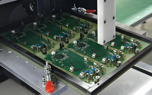
  • Aerospace and Defense – Provides reliability for avionics, satellites, and military equipment.
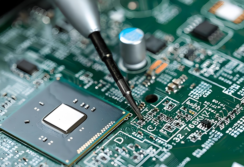
  • Industrial Automation – Supports robotics, sensors, and control systems.

Circuit Card Manufacturer

Why choose EBest Circuit (Best Technology) as your circuit card manufacturer? Choosing the right circuit card manufacturers is critical to ensuring product reliability, performance, and long-term success. At EBest Circuit (Best Technology), we go beyond basic manufacturing to offer comprehensive, high-quality solutions tailored to your exact needs. Here’s why we are the preferred choice for circuit card design, prototyping, and mass production.

1. Full Turnkey Circuit Card Solutions

  • We provide end-to-end circuit card services, from initial design and prototyping to full-scale production. Whether you need a standard circuit card or a customized solution optimized for complex layouts, high-speed signals, or extreme environments, our team ensures seamless development at every stage.

2. Over 18 Years of Manufacturing Excellence

  • With nearly two decades of expertise, we understand the challenges of modern electronics manufacturing. Our in-house engineers specialize in material selection, layout optimization, and high-precision circuit card assembly to deliver superior circuit card performance. Our extensive experience allows us to handle high-frequency, high-power, and multi-layer designs with ease.

3. No Minimum Order Quantity (MOQ) Requirement

  • We support projects of any scale—from small prototype batches for testing to large-volume production for mass deployment. Our flexible manufacturing approach allows you to scale production as needed while maintaining consistent quality at every stage.

4. Certified Manufacturing Facilities for Global Standards

We adhere to strict industry certifications to meet the highest quality and safety standards. Our manufacturing facilities comply with:

  • ISO 9001 – Quality Management System
  • ISO 13485 – Medical Device Manufacturing Standard
  • IATF 16949 – Automotive Industry Standard
  • AS9100D – Aerospace Industry Certification
  • RoHS & REACH Compliance – Environmentally Friendly Production

5. Industry-Specific Expertise & Customization

Each industry has unique requirements, and we tailor our solutions to match specific applications, including:

  • Automotive Electronics – High-reliability circuit cards for vehicle control systems.
  • Medical Devices – Precision circuits for imaging, diagnostics, and monitoring.
  • Aerospace & Defense – High-performance, ruggedized circuit cards for critical missions.
  • Industrial Automation – Custom solutions for robotics, control systems, and sensors.

6. Dedicated Technical Support & Engineering Consultation

  • Our customer-first approach means that you receive expert guidance at every stage. Whether you need design assistance, performance optimization, or troubleshooting, our experienced engineers are available 24/7 to provide technical support and consultation.

FAQs Of Circuit Card

1. What Does a Circuit Card Do?

  • A circuit card connects and supports electronic components, allowing signals and power to flow efficiently between them. It acts as the foundation for any electronic system, ensuring stable operation.

2. What is the Difference Between a Circuit Card and a PCB?

  • A circuit card is a complete electronic assembly that includes a printed circuit board (PCB) and mounted components. A PCB is just the bare board before component placement.
3. How Does a Circuit Card Work?

  • A circuit card works by transmitting electrical signals through its copper traces, enabling communication between different electronic components. This controlled flow allows the device to perform specific functions.

4. How Do You Use a Circuit Card?

  • Circuit cards are integrated into electronic devices during the assembly process. They are placed inside enclosures, connected to other systems, and powered to perform designated tasks.

In a nutshell, a well-designed circuit card is essential for reliable and efficient electronics. From material selection to assembly, every stage plays a crucial role in ensuring performance and durability. If you need expert guidance, EBest Circuit (Best Technology) offers high-quality circuit card solutions tailored to your requirements. Reach out to us at sales@bestpcbs.com for more details.

You may also like

Ceramic PCB Assembly, Ceramic PCB Manufacturing Process
Monday, March 3rd, 2025

Ceramic PCB assembly is becoming a preferred option for industries that demand high thermal conductivity, stable performance, and strong mechanical strength. Compared to traditional FR4 boards, ceramic circuit boards handle heat better, last longer, and work reliably even in extreme environments. That’s why companies in aerospace, automotive, and medical fields turn to this technology for their critical projects.

Ceramic materials offer natural thermal conductivity, so they don’t need extra heat dissipation layers. That means more compact designs without losing efficiency. With ceramic PCB assembly, you also get enhanced reliability when working with high-power components or complex multilayer designs.

Ceramic PCB Assembly, Ceramic PCB Manufacturing Process

What are the substrates for ceramic PCB?

Ceramic PCBs use different substrates depending on the performance requirements of the application. Alumina (Al2O3) is the most common due to its balanced cost and performance. It provides good thermal conductivity, electrical insulation, and mechanical strength. For even higher thermal performance, Aluminum Nitride (AlN) works better. It handles heat far more efficiently, so it’s often used in power electronics or LED applications. Beryllium Oxide (BeO) is another option, though its use is less common due to safety concerns during manufacturing. Still, it offers excellent thermal conductivity when needed.

What are the different types of ceramic PCB?

Ceramic PCBs come in different types to meet various technical needs. Single-layer ceramic PCBs are the simplest and often used when the design doesn’t need many connections. They work well for LED modules or simple power circuits. Double-layer ceramic PCBs offer more flexibility for designs with higher component counts. They can handle complex circuits with better routing options. For advanced applications, multilayer ceramic PCBs provide even more design freedom. These allow for compact, high-density circuits, perfect for RF modules, medical sensors, and aerospace systems.

What are the components of a ceramic PCB?

Ceramic PCBs contain several essential elements that work together to deliver strong performance. The ceramic substrate forms the base, providing heat management, insulation, and structural support. On top of that, copper traces form the electrical connections. These traces are either directly bonded or printed, depending on the design process. The solder mask covers exposed copper to prevent oxidation, though ceramic PCBs sometimes skip this layer to enhance thermal transfer. Finally, components like resistors, capacitors, and ICs are soldered onto the surface to complete the assembly.


Ceramic PCB Assembly, Ceramic PCB Manufacturing Process

How thick is ceramic PCB?

Ceramic PCBs come in different thicknesses to match the needs of the design. Common ceramic substrate thicknesses range from 0.25mm to 1.5mm, depending on the type of material and required mechanical strength. Thin ceramic boards work well when weight reduction matters, such as in aerospace applications. Thicker boards support larger components and provide additional strength. The copper layer itself also varies, usually from 10ÎŒm to 140ÎŒm, depending on current-carrying requirements. Choosing the right combination of ceramic and copper thickness ensures good performance without unnecessary cost.

How to make ceramic PCB?

The ceramic PCB manufacturing process begins with circuit design optimization (e.g., Gerber file preparation) to account for ceramic-specific properties such as thermal expansion and mechanical stability. A ceramic substrate (e.g., alumina or aluminum nitride) is then cut into panels from larger sheets. For copper trace formation, two primary methods are used: ‌Direct Bonded Copper (DBC)‌ involves bonding copper foil to the ceramic under high temperature and pressure, followed by photolithography and etching to define precise circuit patterns, making it ideal for high-power applications. Alternatively, ‌Thick Film Printing‌ uses screen-printing of conductive pastes (e.g., silver-palladium) onto the ceramic surface, which are then sintered at high temperatures to solidify the traces, a cost-effective method for simpler designs. After trace formation, laser drilling creates micro-vias (if required), which are metallized using electroless copper plating to ensure electrical connectivity between layers. Surface finishes like ENIG (Electroless Nickel Immersion Gold) or OSP (Organic Solderability Preservative) are applied to protect copper traces from oxidation. Finally, during assembly, solder paste is deposited, components are placed, and reflow soldering or precision-controlled thermal processes are employed to bond components while minimizing thermal stress mismatch between ceramic and metal parts.

What is the difference between ceramic PCB assembly and FR4 PCB assembly?

Ceramic PCB assembly and FR4 PCB assembly follow some similar steps, but the materials and processes vary a lot. In FR4 PCBs, the fiberglass and epoxy resin form the main structure. These materials offer flexibility, but they can’t handle high temperatures well. Ceramic PCBs use ceramic substrates that naturally conduct heat, so they don’t need extra thermal management layers. This simplifies the design, especially for power electronics. During assembly, soldering ceramic PCBs requires more precision since ceramic expands differently from metals. Specialized equipment helps control the process, ensuring components bond properly without cracking the ceramic. Compared to FR4, ceramic PCB assembly often handles higher temperatures, offers better stability, and lasts longer in demanding environments.

What are the benefits of ceramic PCB?

There are many reasons why companies prefer ceramic PCB assembly for critical projects. Ceramic substrates naturally provide high thermal conductivity, which helps heat-sensitive components stay cool. That extends component life and improves reliability. Ceramic PCBs also offer excellent mechanical strength despite their thin profile. This strength helps them survive harsh conditions, including vibration or sudden temperature changes. Another key benefit is high-frequency performance, which matters for RF applications. Ceramic’s low dielectric loss helps maintain signal integrity. Additionally, ceramic materials resist chemicals, moisture, and aging better than traditional PCB materials. Combined, these benefits make ceramic PCB assembly an excellent choice for high-performance, long-lasting products.

How to choose the best ceramic PCB manufacturer for your project?

Choosing the right ceramic PCB manufacturer makes a huge difference in both quality and cost. Start by checking the manufacturer’s experience with ceramic PCB assembly, especially for your industry. Ceramic handling requires special expertise, so working with an experienced supplier reduces risk. Next, ask about material options. A good manufacturer offers multiple ceramic materials, including alumina, aluminum nitride, and others. Also, review their equipment capabilities. Advanced equipment helps control tolerances and ensures good bonding between ceramic and copper. Don’t forget to check their quality certifications and testing processes. Reliable manufacturers offer full inspection reports, including thermal cycling tests, solderability checks, and X-ray inspections to confirm internal connections. Finally, consider their lead times and ability to support custom designs. Flexibility matters, especially when developing innovative products. By the way, reliable manufacturer is able to promptly reply to inquiries and resolve issues, providing technical support and design consultation to save time and effort in the design and production processes.

Put it in a nutshell, ceramic PCB assembly continues to gain popularity thanks to its unmatched thermal performance, mechanical strength, and long-term reliability. Whether you need multilayer ceramic PCBs, alumina PCBs, or specialized designs for RF or power electronics, ceramic materials offer clear advantages. By partnering with an experienced ceramic PCB manufacturer, you can ensure your products meet high standards and work reliably under tough conditions.

At EBest Circuit (Best Technology), we specialize in China ceramic PCB assembly and wholesale ceramic PCB assembly, delivering quality products for customers worldwide. With more than 18 years of experience, we offer custom designs, fast lead times, and full inspection services to support your most challenging projects. Get in touch with us at sales@bestpcbs.com for any questions or additional information.

You may also like