PCB manufacturing PCB manufacturing
Home > Blog

DFM

Custom Through-Hole PCB Design: Footprints, Assembly and RFQ Checklist
Saturday, July 11th, 2026

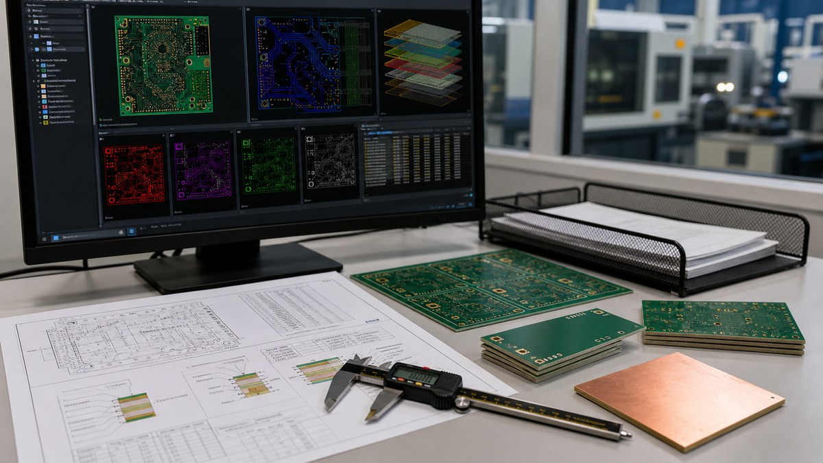
A custom through-hole PCB should be designed from the component leads outward: confirm the real lead dimensions, define finished holes and pads with the fabricator, reserve assembly access, and send complete fabrication and assembly files. The board is only ready for quotation when the manufacturer can identify every drilled hole, plated feature, component orientation, soldering method, inspection requirement, and acceptable substitution without guessing.

This guide focuses on the decisions that connect a through-hole schematic to a manufacturable board and an accurate RFQ. It complements our broader explanation of through-hole circuit board construction, plating, and assembly.

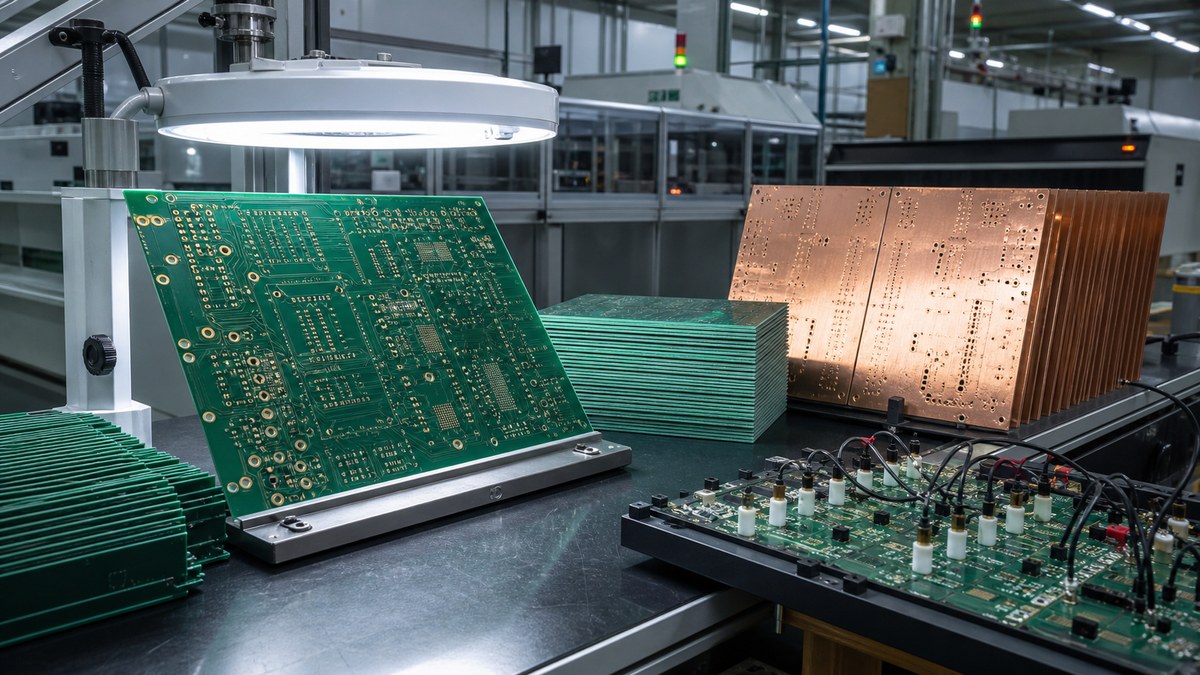
Custom through-hole PCB design with leaded components and plated drill patterns
A useful through-hole PCB design starts with verified component leads, finished-hole requirements, and an assembly plan.

What Is a Custom Through-Hole PCB?

A custom through-hole PCB is a printed circuit board whose plated holes, pads, component footprints, mechanical outline, and assembly method are designed for a specific set of leaded components and operating constraints.

Through-hole technology (THT) places component leads through drilled holes and solders them on the opposite side. It is often selected for connectors, transformers, relays, terminal blocks, large electrolytic capacitors, switches, or other parts that need mechanical retention, serviceability, or compatibility with an existing design. A board can be entirely through-hole or use mixed technology, with SMT parts on one or both sides and selected THT parts added later.

“Custom” does not simply mean a nonstandard outline. The drill table, lead pattern, component height, copper connection, solder access, fixture needs, panel direction, and inspection criteria may all change the manufacturing route.

When Does Through-Hole Technology Make Sense?

Through-hole technology makes sense when component availability, mechanical loading, manual service, high-mass parts, or legacy compatibility matters more than maximum placement density.

Design condition Why THT may help What to verify
Frequently mated connector Leads can transfer mechanical load through the board Connector retention, board support, pad geometry, enclosure load
Large transformer, relay, or capacitor Lead insertion provides stable placement before soldering Mass, vibration, creepage, keepouts, adhesive or mechanical support
Prototype or field-service design Leaded parts may be easier to probe and replace manually Expected rework cycles and pad durability
Legacy product Existing BOM and mechanical interfaces can be retained Lifecycle, alternates, obsolete footprints, documentation quality
Mixed SMT and THT assembly Dense SMT circuitry can coexist with mechanically loaded THT parts Process order, bottom-side clearances, soldering method, fixture access

THT is not automatically more reliable in every design. Reliability depends on the complete interconnect system: component construction, hole and pad design, laminate, copper plating, solder process, mechanical support, cleanliness, inspection, and operating environment.

How Should You Build a Through-Hole Footprint?

A through-hole footprint should be built from the current component drawing, not from a nominal package name or an unverified library symbol.

Check the lead count, pitch, lead cross-section, body size, standoff, insertion side, pin-one convention, polarization, mating direction, tolerance, and any locating or retention features. For rectangular or tab-shaped leads, the diagonal and orientation may control the required hole more than the nominal width.

  • Record the component manufacturer and exact orderable part number.
  • Use the latest mechanical drawing and note its revision.
  • Separate electrical leads from tooling, locating, or non-plated mounting holes.
  • Show polarity and pin-one marks on assembly documentation and silkscreen where space permits.
  • Check the courtyard against neighboring parts, insertion tools, test probes, and enclosure walls.
  • Confirm whether the part must sit flush, use a controlled standoff, or receive extra mechanical support.

A library footprint can be a starting point, but the released footprint should be traceable to a controlled component drawing. This is especially important for connectors and electromechanical parts whose similar product names may hide different pin spacing or retention posts.

How Do You Specify Finished Holes and Pads?

Specify the required finished-hole size and let the PCB fabricator account for its validated drilling and plating process; do not assume the drill tool equals the finished plated hole.

The required clearance depends on the maximum lead envelope, lead shape, component tolerance, insertion method, board fabrication tolerance, plating allowance, and assembly process. The correct value is therefore a design decision to confirm with both the component drawing and the selected manufacturer rather than a universal number copied from another board.

Feature Design input Manufacturing question
Finished plated hole Maximum lead envelope plus validated insertion clearance What finished-hole tolerance can be held for this stackup and quantity?
Pad and annular ring Current, mechanical load, breakout risk, routing space What minimum retained annular ring is supported after registration tolerances?
Thermal connection Required current, heat flow, solderability Will the copper connection cause difficult heating or insufficient solder fill?
Non-plated hole Fastener, locating post, tooling, isolation Is it clearly separated from plated drill data and copper clearances?
Slot or unusual lead Tab dimensions and orientation Is the slot plated, routable, and compatible with the assembly process?

Large copper planes around a THT pad can draw heat away during soldering. Thermal-relief geometry may improve solderability, but it must still meet current and mechanical requirements. Ask the fabricator and assembler to review the actual copper connection instead of applying one default rule to power terminals, signal pins, and structural leads.

What Layout Details Affect Through-Hole Assembly?

Through-hole layout must reserve physical access for insertion, lead trimming, soldering, inspection, rework, and any fixture that supports the board.

Keep polarized parts consistently oriented where practical. Leave enough space to read assembly markings and to reach solder joints without damaging adjacent components. Tall or heavy parts may need spacing from board edges and vibration-sensitive areas. Connectors must be checked in the mated condition, not just as an isolated footprint.

Operator inserting leaded components into a custom through-hole PCB
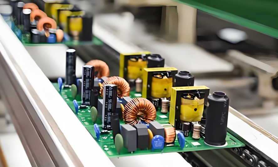
Insertion access, component orientation, lead retention, and fixture clearance should be reviewed before layout release.

For mixed-technology boards, review the entire process sequence. Bottom-side SMT components can interfere with wave pallets or selective-solder nozzles. A component that is easy to place by hand may still block automated soldering or inspection. If prototype and production quantities will use different soldering methods, design for both routes or document the intended change.

Which Soldering Method Should You Plan For?

Choose hand soldering, wave soldering, or selective soldering according to volume, component distribution, thermal mass, bottom-side obstructions, repeatability needs, and fixture cost.

  • Hand soldering suits prototypes, repairs, low volumes, and joints that need individual access, but workmanship consistency and cycle time require control.
  • Wave soldering can process many accessible THT joints efficiently when the underside layout, component orientation, masking, and pallet strategy support the process.
  • Selective soldering targets defined joints or regions and can suit mixed-technology boards where a full solder wave would contact protected areas.

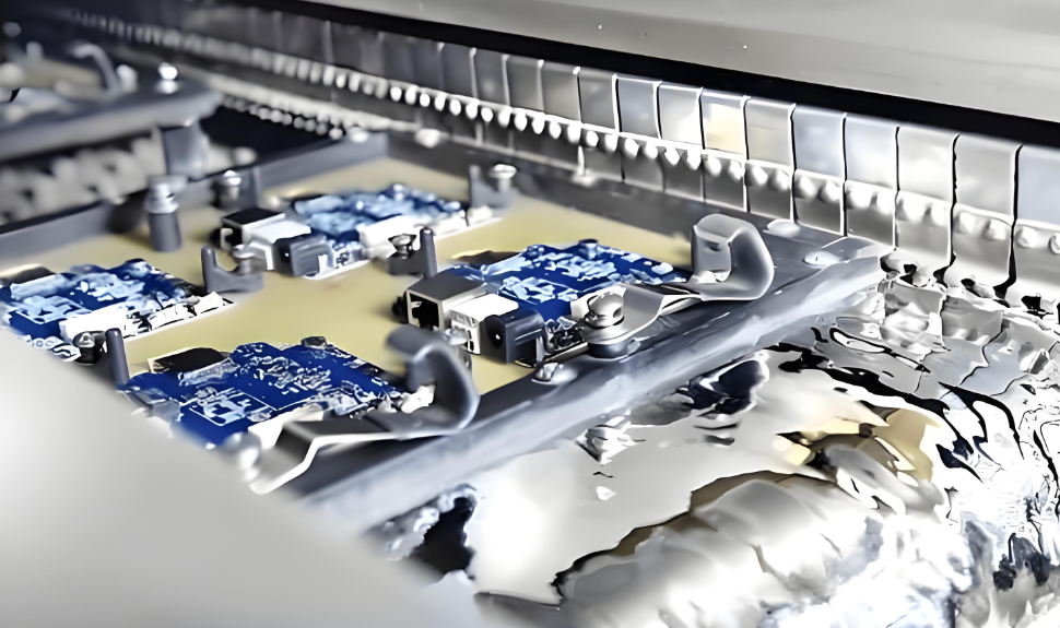
The short comparison below shows the practical difference between wave and selective soldering. It belongs here because the decision directly changes layout clearances, fixtures, process time, and RFQ assumptions.

Wave soldering and selective soldering require different access, masking, and fixture decisions.

When the assembly route is not yet fixed, ask for a DFM review from the intended through-hole assembly service before freezing the bottom-side layout.

What Quality Checks Matter for a Custom Through-Hole PCB?

Quality checks should verify the bare board, component installation, solder joints, cleanliness, electrical function, and any mechanical load that the assembly must carry.

Bare-board review can include drill and plating conformity, continuity and isolation testing, hole position, annular ring, board dimensions, and surface condition. Assembly inspection should check correct components, orientation, seating, lead condition, solder coverage, bridges, void-related concerns where visible or otherwise inspectable, flux residues, and damage from handling or rework.

Microscope inspection of through-hole PCB solder joints
Inspection criteria should match the product class, drawing requirements, acceptance standard, and actual assembly process.

Do not write “IPC Class 2” or “Class 3” on an RFQ without identifying the applicable acceptance document, revision, product requirements, exceptions, and evidence expected from the supplier. If a connector carries repeated mechanical load, a functional or mechanical test may be more informative than appearance alone.

What Causes Common Through-Hole PCB Problems?

Most through-hole problems can be traced to an incorrect footprint, poorly defined hole or copper connection, unstable component retention, unsuitable solder access, uncontrolled thermal demand, or incomplete work instructions.

Observed problem Possible design or process cause Review action
Part will not insert consistently Lead envelope, hole tolerance, pitch, slot orientation, or bent leads Compare the physical part, drawing, footprint, and finished-hole data
Weak or inconsistent solder joint Thermal imbalance, contamination, access, process window, or geometry Review copper connections, materials, cleaning, profile, and acceptance criteria
Component lifts or tilts Poor retention, uneven leads, fixture limits, or solder forces Define seating, lead forming, retention, and fixture method
Pad or barrel damage during rework Excess heat, force, dwell time, or repeated repair cycles Define approved rework method and evaluate repairability during design
Connector fails mechanically Board flex, enclosure load, inadequate support, or incorrect footprint Review the complete mated mechanical system and load path

What Files Are Needed for an Accurate RFQ?

An accurate RFQ needs enough controlled data for fabrication, procurement, assembly, inspection, and acceptance without relying on assumptions.

  • Gerber or ODB++ fabrication data with a clearly identified revision.
  • NC drill files that distinguish plated and non-plated holes, plus slot definitions.
  • Fabrication drawing with board outline, stackup expectations, material, copper, finish, thickness, tolerances, and notes.
  • BOM with manufacturer part numbers, approved alternates, quantities, and do-not-fit status.
  • Assembly drawings for each populated side, including polarity and reference designators.
  • Centroid data for SMT portions of mixed-technology boards.
  • Special instructions for lead forming, insertion depth, standoff, clinching, adhesive, hardware, conformal coating, cleaning, or masking.
  • Inspection and test requirements, including fixtures, firmware, test limits, and acceptance records.
  • Prototype and forecast quantities, packaging needs, and any component consignment plan.

For early builds, a prototype PCB assembly run can confirm footprint fit, insertion access, soldering behavior, and test coverage before production tooling is finalized. If schedule is critical, compare the files and approvals needed for a quick-turn PCB assembly route rather than asking only for the shortest calendar lead time.

Custom Through-Hole PCB Pre-Release Checklist

A design is ready to release when the electrical, mechanical, fabrication, assembly, and inspection data agree with one another.

  1. Match every footprint to the current component drawing and exact orderable part.
  2. Confirm maximum lead dimensions, pitch, orientation, and retention features.
  3. Define finished plated holes, non-plated holes, slots, pads, and copper connections.
  4. Check component body, height, mating, tool, probe, enclosure, and rework clearances.
  5. Select the intended soldering route and review bottom-side access and fixture needs.
  6. Review heavy parts, connectors, board flex, vibration, and mechanical support.
  7. Align fabrication drawing, BOM, assembly drawing, drill data, and revision identifiers.
  8. Define inspection, electrical test, functional test, cleanliness, and acceptance evidence.
  9. Run DFM and assembly review before ordering production quantities.
  10. Validate the prototype with the actual enclosure, cables, mating connectors, firmware, and test fixture.

Frequently Asked Questions

Is a through-hole PCB the same as a plated-through-hole PCB?

Not necessarily. “Through-hole PCB” often describes a board assembled with leaded components, while “plated through-hole” describes a hole with conductive plating connecting pads or copper layers. A board may contain plated through-holes as component holes or vias even when most components are surface mounted.

Can a custom board use both SMT and through-hole components?

Yes. Mixed-technology assemblies are common when dense SMT circuitry must coexist with connectors, relays, transformers, or other leaded parts. The layout must account for process order, bottom-side SMT parts, wave pallets or selective-solder access, inspection, and rework.

How much clearance should a lead have inside a finished hole?

There is no single clearance that fits every component and process. Use the maximum lead envelope, lead shape, insertion method, component tolerance, finished-hole tolerance, plating process, and assembly capability. Confirm the final value with the component drawing and manufacturer before release.

Should the PCB drawing specify drill size or finished-hole size?

The design documentation should clearly communicate the required finished feature and tolerance. The fabricator normally selects a process drill that accounts for plating and its controlled manufacturing route. Ambiguous drill notes can lead to incorrect assumptions, so align the drill files and fabrication drawing.

Are thermal reliefs always required on through-hole pads?

No. Thermal reliefs can improve solderability when a pad connects to a large copper area, but high-current, heat-transfer, or mechanical requirements may call for a different connection. Review electrical and thermal needs together with the solder process.

When is selective soldering better than wave soldering?

Selective soldering is useful when only defined THT joints can contact solder or when bottom-side SMT parts and sensitive areas prevent full wave exposure. Wave soldering can be efficient for layouts designed around broader underside access. Volume, fixture cost, spacing, and thermal demand also affect the choice.

What should be included in a through-hole assembly drawing?

Show component locations, reference designators, insertion side, polarity, pin one, orientation, do-not-fit parts, special seating or standoff requirements, hardware, lead forming, and revision. Add separate controlled instructions when soldering, masking, cleaning, coating, or test requirements need more detail.

How can connector solder joints be protected from mechanical stress?

Design the load path across the connector, board, mounting hardware, enclosure, and cable. Board supports, retention features, fasteners, strain relief, adequate pad and hole design, and controlled mating forces may all matter. Do not expect solder joints alone to absorb repeated external load.

What should be tested on a first prototype?

Verify component fit, polarity, insertion and solder access, electrical continuity, programmed function, connector mating, enclosure fit, temperature behavior, mechanical loads, test-point access, and rework feasibility. Record every change against the controlled design revision before production release.

How do I reduce quotation delays?

Send synchronized fabrication data, drill files, BOM, assembly drawings, test requirements, quantities, and revision identifiers. Flag alternate parts and special processes clearly. A concise question list for unresolved items is better than leaving the supplier to infer missing requirements.

Final Design Decision

A custom through-hole PCB succeeds when the component drawing, finished-hole definition, copper connection, assembly access, soldering route, inspection plan, and RFQ package describe the same product. Resolve those interfaces before production, not during component insertion.

If you are preparing a through-hole or mixed-technology PCB for prototype or production, send the engineering files, BOM, expected quantities, soldering constraints, and test requirements to sales@bestpcbs.com for DFM review and quotation.

You may also like

Free Design for Manufacturing DFM Support, DFM vs. DFMA
Wednesday, April 9th, 2025

What is Design for Manufacturing (DFM)?

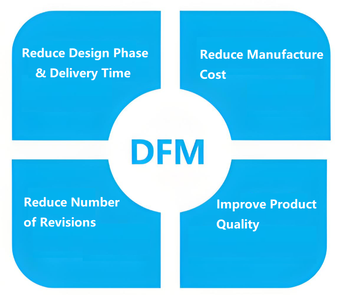
Design for manufacturing, or DFM, is the process of designing products with ease of manufacturing in mind. It focuses on making products that are not only functional but also simple to build. When DFM is done well, it helps reduce production costs, shortens the time to market, and improves quality.

At its core, DFM is about creating designs that match the capabilities of the manufacturing process. Engineers and designers can work together with manufacturers early in the process. So that engineer can identify potential problems before mass production or prototype, save much time for customers.

Free Design for Manufacturing DFM Support, DFM vs. DFMA

3 Goals of DFM

1. Cost Reduction

By optimizing the design, you can reduce waste, material usage, and labor. Simple shapes, fewer parts, and efficient processes lead to lower costs.

2. Faster Production

Well-designed parts are easier to manufacture. This leads to shorter cycle times and quicker delivery. Less rework and fewer changes speed things up too.

3. Improved Product Quality

DFM encourages consistency. It minimizes variation and errors during production. As a result, you get a higher-quality end product that performs reliably.

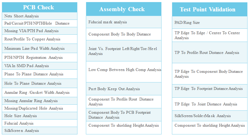
Perform DFM before manufacturing can detect potential defectives that we can’t detect, it covers three aspects, including:

Free Design for Manufacturing DFM Support, DFM vs. DFMA

What are the 5 Principles of Design for Manufacturability?

1. Reduce the number of parts/components

    By simplifying the design, reducing the number of parts can reduce manufacturing costs and complexity and improve production efficiency. For example, combining multiple parts into one not only reduces the chance of errors, but also saves assembly time and development time.

    2. Standardized design

    The use of standardized components and design elements helps to reduce production variability and improve product consistency. Standardized design can reduce design time, improve assembly efficiency, and reduce research and development costs.

    3. Simplify the assembly process

    Considering the convenience of assembly during design can reduce assembly time and cost. Through modular design, the same set of parts can be used alternately, reducing the dependence on specific molds, thereby reducing production costs.

    4. Material selection

    Select the appropriate material to ensure the manufacturability and performance of the product. Reasonable material selection can not only improve product reliability, but also reduce manufacturing costs.

    5. Manufacturing tolerances

    Reasonably set manufacturing tolerances to balance manufacturing costs and product quality. Proper tolerance setting can ensure product quality and reduce production costs at the same time.

    What is the Difference Between DFM and DFMA?

    It’s easy to mix up DFM and DFMA. They’re closely related but serve slightly different purposes.

    DFM (Design for Manufacturing) focuses on manufacturing, refers to the design for manufacturing, mainly focuses on how to simplify the parts processing process through design, reduce the difficulty and cost of manufacturing. Its core goal is to optimize designs and make them easier to manufacture while improving product quality. DFM‌ focuses on parts processing, reducing manufacturing difficulties through design optimization, such as reducing complex processes and avoiding strict tolerances.

    DFMA (Design for Manufacture and Assembly) combines the principles of DFM and DFA (Design for Assembly) to optimize the manufacturing and assembly process of products to reduce costs, increase efficiency and improve product quality. DFMA‌ not only focuses on manufacturing, but also on assembly, emphasizing the comprehensive consideration of manufacturing and assembly optimization in the design stage, such as reducing the number of parts, simplifying the assembly process, etc.

    In short:

    DFM = Can we make this part easily?

    DFMA = Can we make and assemble this product easily?

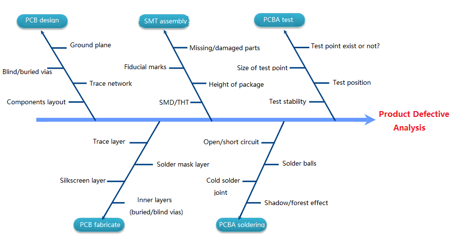
    Common Defective Issues Detected by DFM

    Common Defective Issues Detected by DFM

    How to Perform Design for Manufacturing DFM?

    Performing DFM is not a one-step process. It’s a mindset that should be part of every stage of product development.

    1. Engage Early with Manufacturers

    Bring in manufacturing experts during the design phase. Their insights help prevent rework and delays later.

    2. Evaluate the Design for Each Process

    Check if the design works well with cutting, forming, molding, or other methods. Each process has its strengths and limits.

    3. Reduce Part Counts

    Combine parts where possible. Fewer parts mean fewer connections, less inventory, and easier builds.

    4. Analyze Tolerances

    Use realistic tolerances. Too-tight specs increase cost and difficulty. Focus on where precision is truly needed.

    5. Review Materials and Finishes

    Pick materials that are easy to source and suitable for the environment. Avoid special coatings unless they’re vital.

    6. Prototype and Test

    Use early builds to check for problems. Make improvements based on real data, not just models. DFM is about iteration. Keep refining until the design fits both function and production.

    What Should You Consider When Designing for Manufacture?

    When designing for manufacturing, many small details matter. These are the key areas to watch:

    • Avoid complexity design. Keep PCB simple and easy to shape.
    • Design parts that work well with available tools. Custom fixtures can slow things down.
    • Think about how the part will be handled. Can it be picked up, rotated, and fixed easily?
    • Check how tolerances from one part affect the whole system. Misalignment can come from small errors that add up.
    • Use materials that match the product’s goals—strength, weight, heat resistance—but also consider cost and ease of use.
    • Don’t ask for polished surfaces unless needed. Extra finishing steps raise cost and time.
    • Are the parts easy to source? If not, you may face delays or searching for alternative parts.
    • High-volume parts benefit from different methods than low-volume ones. Tailor your design to the production level.

    Get Free DFM Support with EBest Circuit (Best Technology)

    At EBest Circuit (Best Technology), we support your design goals from the first sketch to the final board. We offer one-on-one support, PCB fast prototyping, and clear communication every step of the way. After getting your design files, we will perform design for manufacturing analysis, and send the report to you to optimize the design. Our service including:

    1. PCB manufacture

    FR-4 PCB, High TG FR-4 PCB, Heavy copper PCB, Impedance control PCB, High frequency PCB, Flexible PCB, Rigid-flex PCB, HDI PCB, Aluminum PCB, Copper based PCB, Ceramic based PCB, high speed PCB, IC substrate

    2. PCB assembly

    SMT, DIP, reflow soldering, Wave soldering, Hand soldering, Mixed assembly, wire harness assembly, PCBA testing, box building assembly

    3. Components sourcing

    Firsthand components, original manufacturers, BOM checking, components sourcing, IQC checking, ISO9001 certificated

    4. PCBA design and duplication

    Hardware engineers, Software engineers, Schematic design, PCB layout, Software development, PCBA duplication

    Whether you need help choosing the right PCB & PCBA manufacturer or searching for a cost-effective solution, we’re here. In our next article, we will share acknowledges about design for assembly (DFA), if you are interested about it, please collect our website or leave your message at comments.

    You may also like