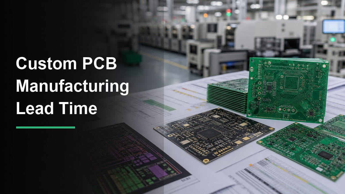
Custom PCB manufacturing lead time is the time from approved production files and quote confirmation to finished boards or assembled PCBAs ready for shipment. It is not set only by layer count. File quality, material availability, surface finish, copper weight, impedance control, component sourcing, testing scope, production queue and shipping route can all add or remove days.
For buyers, the practical question is not “what is the fastest possible PCB lead time?” The better question is “what information does the factory need to confirm a reliable lead time for this exact board?” A simple FR4 prototype with complete Gerbers can move quickly. A custom PCB with HDI, controlled impedance, special laminate, heavy copper, tight drilling, turnkey assembly or functional testing needs a more careful schedule.
What Counts as Custom PCB Manufacturing Lead Time?
Custom PCB manufacturing lead time should be counted after the supplier has approved the production data, confirmed materials and accepted the order, not from the first email.
A realistic timeline usually includes engineering review, quotation clarification, material preparation, bare board fabrication, surface finish, electrical test, optional assembly, final inspection, packing and logistics. If the project includes turnkey PCBA, component sourcing and incoming parts inspection must be counted separately from bare PCB fabrication.
This is why two boards with the same layer count can have different schedules. A standard 4-layer FR4 board with common finish may be simple. A similar-looking 4-layer board with unusual thickness, special copper, impedance coupons, tight annular rings, press-fit connectors or high-reliability testing may need more review and queue time.
Typical Lead Time Stages Buyers Should Separate
The most useful lead time estimate separates engineering review, PCB fabrication, assembly, testing and shipping instead of giving one vague number.
| Stage | What Happens | Common Delay Trigger | Buyer Action |
| Engineering review | Gerber, drill, stackup, drawing, BOM and assembly data are checked. | Missing notes, unclear tolerances, mismatched drill files or incomplete BOM. | Send a complete file package and answer DFM questions quickly. |
| Material preparation | Laminate, copper, prepreg, solder mask and components are reserved. | Special laminate, high Tg, RF material, ceramic substrate or allocated components. | Approve alternates early and confirm critical material rules. |
| PCB fabrication | Imaging, etching, lamination, drilling, plating, solder mask and finish are completed. | HDI, buried vias, thick copper, tight spacing, unusual finish or panel constraints. | Keep the first build inside standard capability when schedule matters. |
| PCBA assembly | Stencil, SMT placement, reflow, through-hole work, cleaning and inspection are performed. | Long-lead components, BGA/X-ray needs, mixed SMT/THT, fixture setup or programming. | Confirm BOM availability and provide placement, polarity and test notes. |
| Inspection and logistics | AOI, electrical test, visual inspection, packing and shipment are arranged. | Extra test reports, rework, customs documents or remote shipping destination. | Define required reports and shipping method before production starts. |
Files That Shorten or Delay a Custom PCB Schedule
Complete files shorten lead time because the factory can quote, review and release production without repeated clarification.
For bare PCB fabrication, send Gerber or ODB++ files, NC drill files, board outline, stackup requirement, copper weight, board thickness, solder mask color, silkscreen color, surface finish, impedance notes, controlled-depth drilling notes and any special acceptance criteria. For PCBA, add BOM, centroid or pick-and-place file, assembly drawing, polarity notes, firmware or programming instructions, and test requirements.
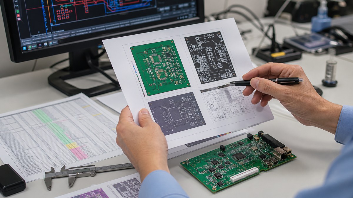
A common delay is a file set that looks complete but has contradictions. Examples include a board outline that does not match the mechanical drawing, a BOM package that does not match the centroid file, a stackup note that conflicts with impedance requirements, or a surface finish choice that is not suitable for the component package. These issues should be solved before the purchase order is treated as production-ready.
Board Complexity Has More Impact Than Board Size Alone
Lead time usually increases when the board requires more controlled process steps, tighter inspection or less common materials.
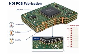
Layer count matters, but it is only one part of the schedule. HDI microvias, blind or buried vias, sequential lamination, heavy copper, fine line and space, controlled impedance, unusual thickness, rigid-flex construction and special surface finishes can all add review and production time. If a project needs HDI density, review the board against realistic HDI PCB manufacturing limits before asking for rush delivery.
Material choice also matters. Standard FR4 is usually easier to schedule than a special laminate, ceramic substrate, metal core PCB, RF material or high-temperature stackup. If standard FR4 is acceptable, the FR4 printed circuit board route may reduce sourcing risk. If the design needs special thermal, high-frequency or structural behavior, lead time should include material confirmation.
PCBA Lead Time Depends on Components, Not Only Assembly Speed
For turnkey PCBA, component availability often controls the real delivery date more than placement speed.
A factory may be able to assemble a small batch quickly once all parts are ready, but that does not mean every assembled board can ship quickly. Long-lead ICs, connectors, magnetics, sensors, relays, custom cables, displays and odd passives can delay the start of assembly. If the BOM has obsolete, allocated or region-specific parts, schedule risk should be discussed before the order is placed.
When schedule matters, confirm whether the supplier can support component sourcing, approved alternates, incoming inspection and shortage reporting. A practical BOM review should identify no-stock items, risky single-source parts, package mismatches and parts that require programming or special handling.
When Quick-Turn PCB Manufacturing Is Realistic
Quick-turn service is realistic when the design uses available materials, complete files and a process flow that fits the factory queue.
Fast schedules work best for simple prototypes, standard materials, small or medium panel sizes, common finishes, clean drill data, no unresolved DFM issues and components that are already in stock. A quick-turn request becomes less reliable when the board needs special laminate, multiple lamination cycles, unusual solder mask, tight impedance tolerance, large panels, heavy copper, fixture-based testing or long-lead components.
For assembled prototypes, a dedicated prototype PCB assembly flow can help engineering teams validate a design before locking mass production. If the project must move from prototypes into larger volumes, quick turn PCB assembly should be planned with component supply and test coverage in mind.
Rush Fees Do Not Fix Every Lead Time Problem
Expedited service can compress queue time, but it cannot remove engineering, material or component constraints that still need resolution.
Rush delivery is most useful when the files are clean and the process is standard. It is less useful when the supplier still needs to clarify impedance, stackup, plating, tolerances, test methods, part substitutions or acceptance criteria. Paying for speed before the file package is stable can create rework rather than faster delivery.
A better approach is to ask the supplier which step controls the schedule. If the answer is material sourcing, choose an available material or accept a longer lead time. If the answer is DFM risk, revise the design. If the answer is component shortage, approve alternates or split the build. If the answer is production queue, expedited service may help.
How to Prepare an RFQ for a Reliable Lead Time
A lead-time-ready RFQ should let the supplier quote the board without guessing about design intent, assembly scope or acceptance criteria.
- Send the final Gerber or ODB++ package, NC drill files and board outline.
- Include stackup, copper weight, board thickness, material preference and surface finish.
- Mark impedance, controlled-depth drilling, press-fit holes, castellations or edge plating if used.
- For PCBA, send BOM, centroid file, assembly drawing, polarity notes and testing requirements.
- State the target quantity, prototype or production purpose, required delivery date and shipping country.
- List any parts that cannot be substituted and any parts where alternates are allowed.
- Ask the supplier to separate fabrication, component sourcing, assembly, testing and shipping time.
Lead Time Risk Checklist Before You Approve Production
Before approval, check the schedule against the real manufacturing risks instead of accepting a single optimistic delivery date.
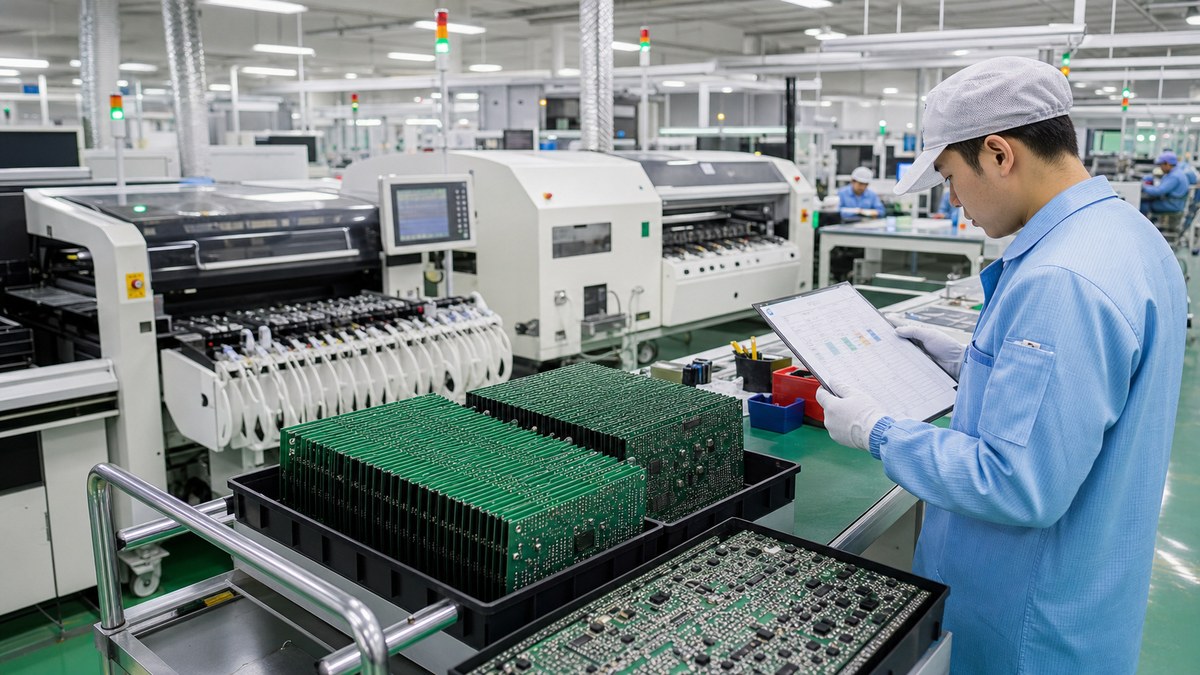
- Are all production files approved and version-controlled?
- Are laminate, copper, solder mask and surface finish available?
- Do all critical components have stock, alternates or confirmed purchase dates?
- Does the board need impedance testing, flying probe, fixture test, AOI, X-ray or functional test?
- Does the first article require engineering approval before the full batch continues?
- Are packaging, labeling, customs documents and shipping method already defined?
- Is the promised date based on working days, calendar days or shipment date?
How to Reduce Custom PCB Manufacturing Lead Time Without Raising Risk
The safest way to reduce lead time is to remove uncertainty before production starts.
Use standard materials when possible, keep the first prototype inside common capability, avoid unnecessary special finishes, release a clean BOM, allow qualified alternates and answer DFM questions fast. For PCBA, order critical long-lead components early or let the supplier source parts before the bare boards are finished. For repeat builds, keep the same approved stackup, finish, stencil and test plan unless a change is necessary.
Do not shorten lead time by skipping review on a high-risk board. A missed annular ring issue, wrong footprint, unavailable connector or unclear test requirement can cost more time than a proper review. Good suppliers should be willing to explain the bottleneck instead of only quoting the fastest possible date.
Supplier Questions That Reveal Whether the Schedule Is Reliable
Ask schedule questions that force the supplier to show where the lead time comes from.
- When does your lead time clock start: quote approval, payment, file approval or material arrival?
- Which step is the current bottleneck for this board?
- Are the laminate, solder mask, surface finish chemicals and critical components already available?
- What changes would shorten the lead time without weakening reliability?
- Does the quote include electrical test, AOI, X-ray, functional test or only basic inspection?
- Will the promised date be shipment date or arrival date?
- What happens if DFM review finds a file issue after order approval?
FAQ About Custom PCB Manufacturing Lead Time
These answers are written for buyers preparing an RFQ, not for one fixed factory schedule.
How long does custom PCB manufacturing take?
It depends on board complexity, material availability and whether assembly is included. Simple prototypes can move much faster than HDI, rigid-flex, ceramic, heavy copper or fully assembled PCBAs. Treat any published number as a starting point and ask for a quote based on your actual files.
When should I start counting PCB lead time?
Count lead time after production files are approved, the order is confirmed and required materials or components are available. Early emails, incomplete Gerbers or unresolved BOM questions should not be treated as production time.
What files are needed to confirm custom PCB lead time?
For bare boards, send Gerber or ODB++ files, drill files, board outline, stackup, material, thickness, copper weight and finish. For PCBA, add BOM, centroid file, assembly drawing, polarity notes and test requirements.
Does PCBA always add more lead time than bare PCB fabrication?
Usually yes, because assembly needs stencil preparation, component sourcing, placement, soldering, inspection and sometimes testing. The largest delay is often component availability, not the placement process itself.
Can I reduce lead time by using standard FR4?
Often yes. Standard FR4, common board thickness, common copper weight and common surface finish are easier to schedule than special laminate, ceramic, RF material, metal core, rigid-flex or unusual process requirements.
What makes HDI or rigid-flex boards slower?
HDI and rigid-flex designs may need sequential lamination, laser drilling, tighter registration, controlled impedance, special materials and extra inspection. These steps are useful, but they should be planned instead of treated like standard quick-turn FR4 work.
Do rush fees guarantee delivery?
No. Rush fees may reduce queue time, but they cannot remove material shortages, unresolved DFM issues, unavailable components or unclear test requirements. Ask which step controls the schedule before approving an expedite charge.
How can I avoid delays after placing the order?
Freeze the file revision, respond to DFM questions quickly, approve part alternates early, confirm test requirements and avoid changing quantity, finish or shipping method after production starts.
Should I split prototypes and production into separate orders?
For new designs, yes in many cases. A prototype order can validate the layout, BOM, assembly process and test plan before a larger production batch. This reduces the risk of repeating an error at volume.
What should a supplier include in a clear lead time quote?
The quote should separate engineering review, material or component sourcing, bare PCB fabrication, assembly, inspection, packing and shipping. It should also state whether the date means completion, shipment or delivery.
Final Buying Advice
Custom PCB manufacturing lead time is predictable when the supplier sees the full design, confirms materials and separates each production stage. Before approving a rush order, ask what is slowing the schedule and whether a file, material or BOM change would reduce risk. If you are planning PCB fabrication, turnkey PCBA, prototypes or mass production, send your Gerber, BOM and assembly files to the Best Technology engineering team at sales@bestpcbs.com for a lead time and quotation review.
You may also like





Tags: Custom PCB, lead time, pcb manufacturing, Quick Turn PCB