
PCB CAM work outsourcing means assigning manufacturing front-end engineering to a specialist team that audits customer data, prepares factory tooling, resolves DFM questions, and releases controlled CAM outputs. It should not give the CAM provider silent authority to change circuit function, approved dimensions, stackup intent, impedance, materials, or customer-controlled features.
The safest arrangement defines inputs, permitted transformations, approval thresholds, output files, revision records, and the factory handoff before work begins.
Can you prove which geometry came from the customer, which CAM edits were manufacturing-only, and which changes received approval?
Without that trace, a repaired pad, moved copper feature, modified solder mask, changed drill, altered panel, or adjusted impedance geometry can become an undocumented product change.
EBest Circuit reviews the released PCB package through manufacturing CAM before fabrication.
Send Gerber or ODB++, NC drill/route data, fabrication drawing, stackup, material and copper requirements, impedance notes, netlist data where available, quantity, panel/delivery preference, test scope, and target schedule. Open questions and any change requiring customer authority must be resolved against the actual construction.
What PCB CAM Outsourcing Covers After Design Release
CAM sits between customer design outputs and executable factory data. Typical front-end work includes layer identification, format and polarity checks, drill/tool analysis, netlist comparison, DFM analysis, stackup and impedance coordination, solder-mask and legend checks, panelization, coupons, tooling features, rout/V-cut data, factory compensation, and release documentation.
CAM may repair data artifacts or apply approved manufacturing compensation, but it does not validate circuit function. The customer remains responsible for design intent, electrical behavior, safety, controlled dimensions, and the approved revision.
Audit the Incoming Data Before CAM Work Starts
The first deliverable should be an input-status report, not a tooled panel. Confirm:
- file set, revision, units, format, naming, and checksum;
- layer count, copper/mask/legend/paste/mechanical roles, polarity, and alignment;
- plated/non-plated drills, slots, countersinks, depth-controlled features, and drill pairs;
- outline, dimensions, tolerances, cutouts, edge treatment, V-cuts, and routed tabs;
- stackup, finished thickness, copper, material, Tg/other properties, and special construction notes;
- impedance targets, tolerance, layers, references, line classes, and coupon expectations;
- netlist availability and whether comparison is permitted/required;
- panel, tooling, marking, date/lot code, testing, reports, quantity, and delivery requirements.
The PCB fabrication drawing guide shows which requirements should not be left to filenames or assumptions.
Separate CAM Corrections From Customer Design Changes
Classify every issue before editing.
| Issue class | Example | Who approves | Required record |
|---|---|---|---|
| Data clarification | Unknown mechanical layer or unit ambiguity | Customer data owner | Question and confirmed interpretation |
| Routine factory transformation | Documented process compensation that preserves finished geometry | Defined by approved factory process | CAM rule/version and output trace |
| Manufacturability correction | Mask bridge, annular ring, copper-to-edge, drill or rout conflict | Customer unless pre-authorized threshold exists | Before/after view and disposition |
| Design change | Moved trace, pad, component land, net, hole, outline or controlled dimension | Customer design authority | Revised source/release or formal deviation |
Never let a small geometric delta bypass the approval rule merely because CAM software can repair it automatically.
12 Front-End CAM Checks Before a PCB Job Is Tooled
- Layer mapping, polarity, registration origin, units, and scaling.
- Customer revision consistency across every file and drawing.
- Netlist extraction and comparison to supplied reference data.
- Minimum conductor width/spacing by copper layer and construction.
- Annular ring, drill-to-copper, breakout risk, and finished-hole allowance.
- Copper-to-profile, slot, cutout, V-cut, and scoring clearances.
- Solder-mask openings, dams, via treatment, and exposed copper intent.
- Legend-to-pad/mask/profile conflicts and required marking content.
- Plane polarity, thermal connections, isolated copper, and unintended islands.
- Impedance features, reference layers, stackup consistency, and coupons.
- Panel rails, spacing, tabs, tooling holes, fiducials, coupons, and depanelization.
- Factory electrical test, inspection, traveler, output archive, and approval status.
Use a broader PCB DFM checklist to connect these CAM checks to design and assembly consequences.
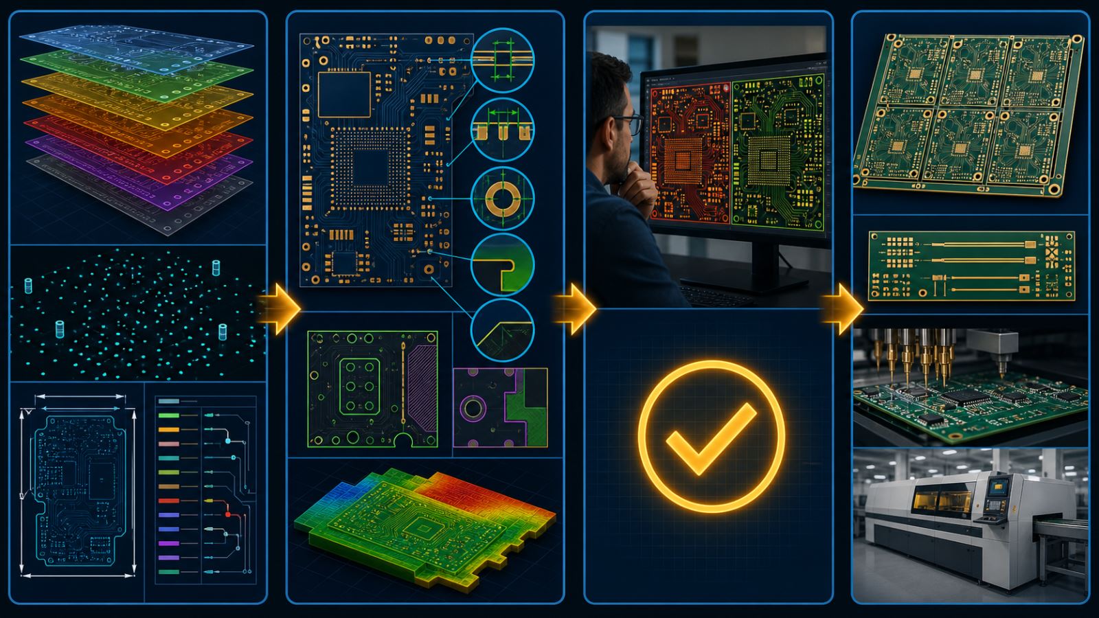
Panelization and Tooling Data Need Customer-Supplier Alignment
Panelization changes manufacturing, assembly, test, handling, and depanelization risk. The CAM scope should identify who owns the customer array, fabrication panel, assembly panel, rails, breakaway features, coupons, fiducials, tooling holes, bad-mark strategy, serial/lot marking, and delivered format.
Consider board geometry, component overhang, edge clearances, selective solder or fixture access, conveyor support, warpage, copper balance, paste/placement needs, test fixtures, depanelization stress, and packaging. A panel optimized only for fabrication may be awkward for assembly; a customer array may need a larger factory production panel around it.
Stackup and Impedance Changes Must Be Controlled
CAM cannot safely treat stackup and impedance as independent post-processing. Material availability, dielectric thickness, copper, finished thickness, layer count, via structures, reference planes, line geometry, etch compensation, and coupon design interact.
If the factory proposes a production stackup, return the layer structure, materials, nominal dielectrics/copper, impedance geometry, targets/tolerances, coupons, and affected nets or classes for customer confirmation. Preserve the approved version with the job. For complex builds, use the HDI process guide to review sequential lamination and microvia dependencies.
Find front-end data conflicts before they become factory assumptions.
Send the controlled PCB release, fabrication drawing, stackup, impedance notes, netlist data, panel requirements, quantity, test scope, and target schedule. EBest Circuit can review the manufacturing inputs and return project-specific questions before fabrication.
Gerber/ODB++ | Drills | Drawing | Stackup | Netlist | Panel | Test
Build an Approval Loop That Leaves an Audit Trail
Each open issue needs an owner, evidence, disposition, and released revision. Use screenshots or marked views, coordinates, layer names, rule/value, risk, proposed action, and response deadline. Record accept, reject, supply revised data, or approve deviation.
Do not rely on chat fragments detached from the job. Freeze customer inputs, CAM software/rule version, reviewed output, approved changes, production stackup, panel drawing, test data, and final release status. When customer files change, restart affected comparisons rather than overwriting the old result.
How to Evaluate a PCB CAM Outsourcing Provider
- Can it preserve the customer baseline and produce before/after evidence?
- Which formats, netlists, stackups, impedance models, panel rules, and factory systems are supported?
- How are automated edits classified and approved?
- Can senior CAM engineers review HDI, flex/rigid-flex, RF, heavy copper, controlled depth, and unusual outlines when relevant?
- How are customer data, IP, access, subcontracting, retention, and deletion controlled?
- What checks are automated, what receives human review, and what remains customer responsibility?
- How are response time, revision count, error correction, escalation, and factory feedback handled?
- Does the final archive let another qualified factory or engineer reproduce the approved job?
Final CAM Deliverables the Factory Should Preserve
The archive should show the path from customer release to factory release. Preserve the original input manifest and checksums, input audit, extracted/reference netlists, DFM report, issue/disposition log, approved stackup and impedance/coupon data, panel/tooling drawing, rout/V-cut data, electrical-test data, customer approvals, factory CAM outputs, software/rule versions, and traveler/release record.
If an intelligent package is used, the IPC-2581 guide explains why machine-readable data still needs revision and viewer checks.
How EBest Circuit Uses CAM Review Before Fabrication
EBest Circuit uses manufacturing front-end review to clarify the actual board construction before production. Available checks can cover layer/data consistency, drills, spacing, annular features, copper-to-profile, mask and legend, stackup, impedance notes, panel requirements, fabrication drawing, and requested test/documentation scope.
Capability is confirmed for the actual combination of material, layers, copper, thickness, holes/vias, geometry, finish, tolerance, panel, quantity, and schedule. A CAM suggestion that changes customer-controlled intent is returned for approval rather than silently treated as a routine repair.
FAQ About PCB CAM Outsourcing
What is PCB CAM engineering?
It is the manufacturing front-end work that audits released PCB data, applies controlled factory transformations, performs DFM checks, creates panel/tooling/test data, and releases executable fabrication information.
Is PCB CAM the same as PCB design?
No. PCB design creates circuit and physical layout intent. CAM prepares approved design outputs for manufacturing and should not change product intent without authority.
Why outsource PCB CAM work?
Companies may need specialist capacity, 24-hour coverage, format expertise, or standardized front-end processing. Value depends on accuracy, traceability, approval control, security, and factory integration.
What files does PCB CAM need?
Typically Gerber/ODB++, drills/routes, fabrication drawing, stackup, material/copper and impedance notes, netlist data, panel requirements, tests, quantity, and schedule.
Can CAM engineers repair Gerber data?
They can correct agreed manufacturability or data issues, but the change class and approval threshold must be defined. Design-intent changes require customer authority.
What is the difference between a customer array and a fabrication panel?
A customer array is the delivered multi-board format. A fabrication panel may place one or more arrays/boards within factory rails, coupons, tooling, and process spacing.
How do I verify CAM output?
Compare it with the frozen input, review the DFM/change log, inspect layers/drills/outline/panel in an independent viewer, compare connectivity, and approve stackup, impedance, and controlled changes.
Make every front-end correction visible before production starts.
Email the released data and identify the approved revision, stackup, impedance, panel, test and documentation requirements. EBest Circuit can confirm the project-specific CAM review and PCB quotation scope.
Baseline | DFM | Approvals | Stackup | Panel | Test | Release
You may also like








Tags: design for manufacturing, pcb design, pcb manufacturing