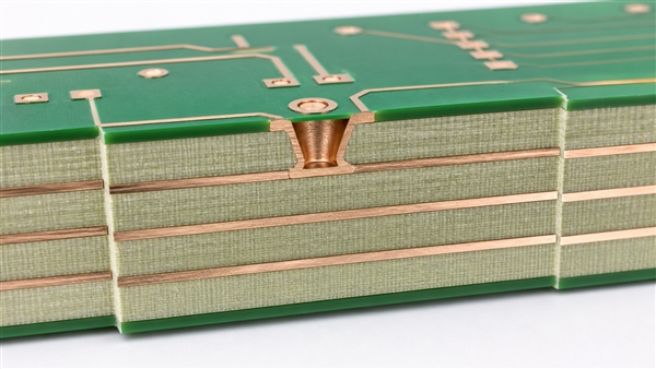
An HDI PCB manufacturer builds high-density interconnect circuit boards using fine lines, microvias, blind or buried vias, tighter routing, sequential lamination and controlled stackups. For engineers and buyers, the key question is not whether a supplier says “HDI” on a page. The key question is whether the supplier can review the stackup, via structure, line width, dielectric thickness, impedance, BGA escape route, testing plan and RFQ files before production.
This guide explains how to compare HDI PCB manufacturers for prototype and production projects. Specific process values are based on Best Technology / bestpcbs capability records where available, and unsupported claims about guaranteed yield, certification, equipment count or lead time are intentionally avoided.
HDI PCB Manufacturer at a Glance
A reliable HDI PCB manufacturer should connect microvia fabrication, fine-line imaging, lamination control, impedance planning, drilling, plating, inspection and test into one manufacturable stackup. HDI failures often start with stackup or via assumptions, not with the final quote number.
| HDI area | What to confirm | Why it matters |
|---|---|---|
| Via structure | Blind vias, buried vias, microvias, stacked or staggered vias | Controls routing density, reliability and lamination steps. |
| Fine lines | Inner/outer line width and spacing by copper thickness | Determines whether BGA escape and dense routing are realistic. |
| Stackup | Layer count, dielectric thickness, HDI build-up, material and impedance | Controls signal integrity and manufacturability. |
| Test plan | E-test, impedance coupon, microsection or functional checks when needed | Prevents hidden defects from moving into assembly. |
Is Your HDI PCB Quote Missing Microvia and Stackup Risk Review?
HDI PCB buyers need early review because microvias, fine lines, BGA escape and sequential lamination can create hidden manufacturing risk.
| Customer Pain Point | Project Risk | How bestpcbs Helps |
|---|---|---|
| Microvia structure is not defined clearly | Stacked, staggered, blind or buried via choices can change cost and reliability | bestpcbs reviews the via plan, layer build-up and drill data before treating the quote as final. |
| Fine-line routing is close to the process limit | Dense BGA escape can fail DFM or require layout changes | bestpcbs checks line width, spacing, copper and critical routing areas during file review. |
| Impedance and stackup notes are missing | Signal performance and thickness targets may not match fabrication assumptions | bestpcbs asks for stackup, dielectric, impedance and material expectations before production. |
| Testing scope is unclear | Hidden opens, shorts or via issues may be found too late | bestpcbs confirms electrical test, impedance coupon or project-specific inspection needs during RFQ review. |
HDI Buyer Priorities Before Sending an RFQ
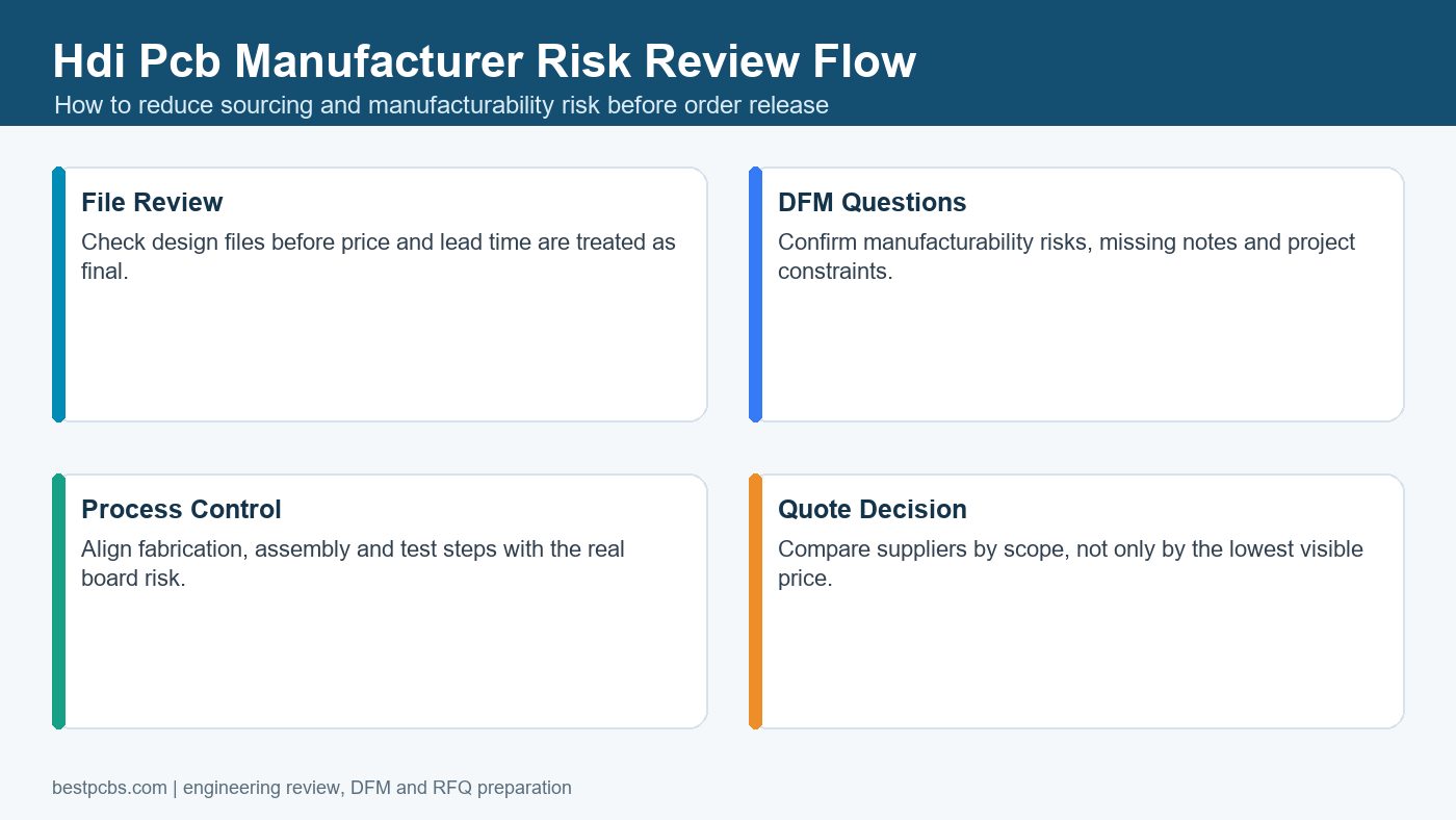
HDI PCB buyers should confirm microvia structure, build-up sequence, fine-line limits, impedance needs and inspection expectations before treating a quote as final. A supplier may accept the files quickly, but hidden stackup or via risks can still appear during fabrication.
Prepare clear notes for blind or buried vias, stacked or staggered microvias, BGA escape areas, copper requirements, controlled impedance and test scope. A useful HDI supplier will review these details early instead of quoting only from the board outline and layer count.
HDI PCB Capabilities Buyers Should Verify
Before selecting an HDI PCB manufacturer, verify layer count, via size, line width, board thickness, surface finish, solder mask limits and impedance needs against the final design. HDI capability depends on the exact stackup, not one universal number.
| Capability item | Verified bestpcbs reference | RFQ note |
|---|---|---|
| FR4 layer count | 1-10 layers under normal range, with 10-32 layers listed as special capability; high-Tg is required for 8 layers and above in the referenced sheet. | Send layer count, material, Tg need and board thickness together. |
| Laser blind / buried vias | 0.1 mm is listed for laser buried/blind vias. | Confirm aspect ratio, pad design and plating expectations. |
| Mechanical blind / buried holes | 0.2 mm normal and 0.15 mm special values are listed. | Do not mix this with laser microvia rules without review. |
| Fine line / spacing | 1/2 oz inner layer 4/4 mil normal and 3/3 mil special; 1/1 oz outer layer 4/4 mil normal and 3/3 mil special. | Check against copper weight and finished plating, not only CAD spacing. |
| Board thickness | Several surface finishes list 0.4-3.5 mm process thickness ranges, with thinner and thicker cases requiring review. | Thin HDI designs need separate stackup confirmation. |
Microvias, Blind Vias and Buried Vias
Microvias, blind vias and buried vias are the core routing tools that make HDI PCB manufacturing different from standard multilayer PCB fabrication. They let engineers escape dense BGAs and reduce board size, but they also add lamination, drilling and plating risk.
Ask the manufacturer whether the design uses one-step HDI, multiple build-up layers, stacked microvias, staggered microvias, via-in-pad, buried vias or any-layer structures. The microvia PCB guide is a useful related reference for design-side reliability checks.
HDI Stackup Review Before Quote
An HDI stackup must be reviewed before pricing because layer count, dielectric thickness, via sequence, material and impedance targets change the process route. A quote that ignores stackup assumptions is not a final quote.
Send the full stackup, copper weight, dielectric thickness, via structure, target board thickness and impedance nets. If the design includes high-speed interfaces, RF sections, dense BGA fanout or controlled impedance, the manufacturer should not quote from Gerber files alone. The HDI PCB fabrication guide gives a broader process background.
Fine Lines, BGA Escape and Routing Density
Fine-line HDI design should be checked by copper weight, solder mask, imaging process and finished plating requirements. A layout with tight CAD spacing may still need adjustment for repeatable fabrication.
For dense BGA escape, ask whether the manufacturer needs dog-bone fanout, via-in-pad, stacked vias, staggered vias or extra build-up layers. If the board uses 0.4 mm pitch or smaller BGA packages, provide package drawings and target inspection requirements. The fine-line HDI PCB guide is a related internal resource for this decision.
Materials, Tg and Surface Finish
HDI materials should be chosen by reliability, lamination needs, thickness target, impedance and soldering conditions rather than by price alone. The referenced bestpcbs capability sheet notes that high-Tg material is required for 8-layer and higher FR4 boards in that process table.
Surface finish also affects HDI design. ENIG, OSP, HASL, immersion silver, immersion tin, ENEPIG and hard-gold-related ranges are listed in the capability sheet with process thickness constraints. Buyers should state the final surface finish and assembly requirement in the RFQ instead of leaving it to default assumptions.
HDI PCB Cost Drivers
HDI PCB cost is driven by build-up structure, microvia count, lamination cycles, fine-line yield risk, material choice, impedance control, test requirements and panel utilization. The cheapest quote may be missing one of these assumptions.
| Cost driver | Why it changes price | How to control it |
|---|---|---|
| Build-up layers | More sequential lamination increases process steps. | Use only the HDI structure the design needs. |
| Stacked microvias | They can add reliability and plating requirements. | Use staggered vias where acceptable. |
| Fine lines | Tighter line/space reduces process margin. | Widen escape routes where the component allows it. |
| Testing | Impedance and extra inspection add setup. | Define which nets, coupons and checks are required. |
Prototype and Production HDI Orders
Prototype HDI orders should validate the stackup and via structure, while production orders need stronger controls for repeatability, material approval and test records. A prototype that only proves electrical function may not prove production repeatability.
For prototypes, focus on feasibility, DFM notes, BGA escape, impedance targets and early assembly fit. For production, define revision control, approved materials, acceptance criteria, panelization and any additional test documentation. If assembly is included, connect the HDI quote with the PCBA and PCB assembly service scope.
How to Compare HDI PCB Manufacturers
Compare HDI PCB manufacturers by the quality of their engineering review, not only by their layer-count claims. The best supplier response should identify stackup risks, missing files and assumptions before the job starts.
- Can they review microvia, blind via and buried via structures before quoting?
- Do they explain normal and special process ranges separately?
- Can they support fine-line routing and controlled impedance for the actual copper weight?
- Do they ask for BGA pitch, via-in-pad needs and assembly constraints?
- Do they avoid unsupported promises about yield, lead time or certification?
RFQ File Checklist for HDI PCB Projects
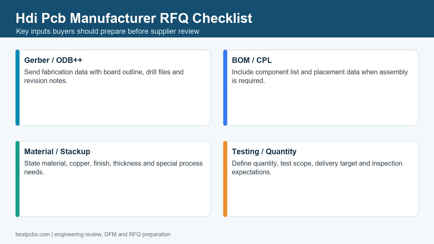
A complete HDI RFQ package should include fabrication files, stackup, via structure, impedance data, material needs, surface finish, quantity and test requirements. Missing stackup or via details can make the first quote unreliable.
| RFQ item | Why it matters |
|---|---|
| Gerber or ODB++ | Defines copper, mask, drill and board outline data. |
| Stackup drawing | Shows HDI build-up sequence, dielectric thickness and copper weights. |
| Drill table | Separates mechanical holes, laser vias, blind vias and buried vias. |
| Impedance requirements | Defines controlled nets, target values and tolerance. |
| BGA and component data | Helps review escape routing and via-in-pad needs. |
| Test and acceptance criteria | Clarifies E-test, impedance coupons, inspection and functional checks. |
Internal Resources for HDI Buyers
HDI buyers should connect service pages, process guides and related supplier-selection articles before sending an RFQ. Useful internal references include the HDI PCB product page, the HDI PCB manufacturer capability page, the any-layer HDI PCB guide, and the multilayer PCB manufacturing checklist.
Common HDI PCB Sourcing Mistakes
Common HDI sourcing mistakes include quoting from incomplete files, ignoring via structure, comparing suppliers with different test scopes, and treating all “HDI” claims as equal. These mistakes create late cost changes and manufacturing delays.
- Do not send only Gerbers when the design depends on sequential lamination.
- Do not assume any-layer, stacked microvia or via-in-pad support without review.
- Do not compare prices unless the same surface finish and test scope are included.
- Do not hide assembly constraints when HDI is used under dense components.
- Do not publish final lead-time expectations before material and stackup confirmation.
Frequently Asked Questions About HDI PCB Manufacturers
What does an HDI PCB manufacturer do?
An HDI PCB manufacturer fabricates high-density interconnect boards using fine routing, microvias, blind or buried vias, controlled stackups and tighter process control than standard PCB fabrication.
Is HDI PCB the same as multilayer PCB?
No. Many HDI boards are multilayer boards, but HDI specifically involves higher interconnect density, often using microvias, blind vias, buried vias or sequential build-up structures.
What files are required for an HDI PCB quote?
Send Gerber or ODB++, drill files, stackup, via structure notes, impedance targets, material requirements, surface finish, quantity, BGA details and test requirements.
Can HDI PCB be assembled by the same supplier?
Yes, if the supplier supports PCBA or turnkey assembly. For dense HDI boards, assembly planning should include BGA placement, via-in-pad assumptions, inspection access and test requirements.
Final RFQ Recommendation
Choose an HDI PCB manufacturer that reviews the stackup, via structure, fine-line routing, material choice, impedance and testing plan before quoting. This reduces the risk of a low initial quote turning into a redesign or delayed build.
For an HDI PCB quotation, send your Gerber or ODB++ files, stackup, drill table, via structure, impedance targets, material requirements, surface finish, quantity, BGA data, BOM, CPL, assembly drawings if needed, test requirements and target lead time to sales@bestpcbs.com. The Best Technology / bestpcbs team can review the package and identify which HDI assumptions need confirmation before prototype, pilot or production release.