PCB manufacturing PCB manufacturing
Home > Blog

pcb manufacturing

PCB Fabrication Manufacturer Selection Guide
Wednesday, July 15th, 2026
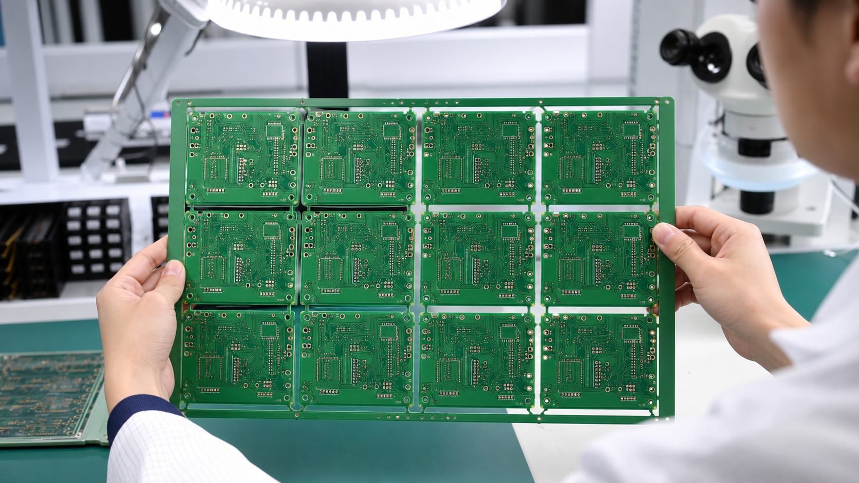
PCB fabrication manufacturer inspecting bare circuit boards

A PCB fabrication manufacturer builds the bare printed circuit board from your design files, then verifies that the board can support assembly, testing, and the product environment. For buyers, the strongest supplier is not simply the one with the lowest board price. It is the manufacturer that can review your files, explain process risks, and help prevent expensive surprises before production starts.

This guide explains how to compare PCB fabrication manufacturers when you need prototype boards, low-volume builds, or production-ready bare boards. It focuses on DFM review, materials, surface finish, quality checks, quotation files, and supplier questions that help engineers and purchasing teams choose a safer manufacturing path.

PCB Fabrication Manufacturer at a Glance

A PCB fabrication manufacturer converts Gerber or ODB++ data into finished bare boards through material preparation, imaging, etching, drilling, plating, solder mask, surface finish, routing, inspection, and electrical testing. The exact flow changes with board type, layer count, material, copper, finish, and special process requirements.

Buyer need What the manufacturer should check Why it matters
Prototype board Files, outline, drill data, solder mask, quick DFM issues Finds design problems before assembly or product testing.
Engineering build Stackup, copper, impedance, material, finish, panelization Improves repeatability before volume release.
Production board Quality plan, test coverage, packaging, revision control Reduces field risk and purchasing uncertainty.

When You Need a Fabrication Manufacturer Instead of Only a Broker

You need a fabrication-focused manufacturer when your board has engineering risk that should be reviewed before production, not only priced from uploaded files. A broker or trading path may be acceptable for simple boards, but it can add communication gaps when the design needs stackup review, material confirmation, controlled impedance, heavy copper, special finish, or strict inspection requirements.

Ask who performs DFM review, who confirms process capability, who answers engineering questions, and who owns quality feedback if a board issue appears after assembly. For buyers who also need components mounted, the PCBA and PCB assembly service page is a useful companion reference.

DFM Review Before Fabrication

DFM review checks whether the design can be fabricated consistently with the selected material, copper, holes, clearances, surface finish, and panel requirements. It should happen before the board enters production because late corrections can change cost, lead time, and risk.

Review points include trace and spacing, annular ring, via type, drill-to-copper clearance, solder mask dams, copper balance, board edge clearance, slot notes, controlled impedance details, panel tooling, and whether drawings match Gerber data. For a deeper design-side checklist, see the PCB design for manufacturability checklist.

PCB Types and Materials to Confirm

The board type and material should be confirmed before quoting because they affect process route, manufacturability, inspection, and assembly behavior. Common projects may use FR-4, while other designs may require high-Tg material, metal-core PCB, ceramic substrate, high-frequency material, flex, rigid-flex, or heavier copper.

Do not publish or accept exact capability numbers unless they are checked against the latest Best Technology process capability files and the specific project notes. For RFQ purposes, send the intended material, board thickness, copper weight, surface finish, layer count, impedance need, and operating environment so the manufacturer can confirm feasibility instead of guessing.

Layer Count, Stackup and Controlled Impedance

Stackup decisions should be treated as manufacturing requirements, not only layout preferences. Layer count, dielectric thickness, copper distribution, reference planes, impedance targets, and finished board thickness can affect performance and fabrication consistency.

If impedance matters, provide impedance values, tolerance expectations, trace geometry assumptions, and stackup notes. If the design is not locked, ask the manufacturer to review the proposed stackup before routing or before final release. This helps avoid a board that is theoretically correct but hard to manufacture repeatably.

Surface Finish and Solderability Choices

Surface finish should be selected according to component pitch, soldering method, shelf life, cost target, and reliability needs. The right finish for a basic prototype may not be the right finish for a fine-pitch, production, or connector-heavy board.

Question Why to ask it
Will the board use fine-pitch or BGA components? Pad flatness and solderability become more important.
How long may boards wait before assembly? Shelf-life expectations can affect finish choice.
Are edge connectors or special pads used? Some finishes or process notes may need early confirmation.

Quality Control and Electrical Testing

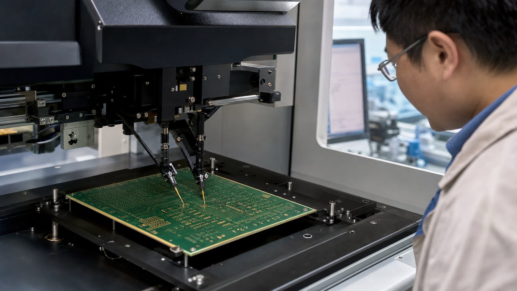
A suitable PCB fabrication manufacturer should explain what inspection and testing apply to your board, rather than leaving quality as a vague promise. Bare board checks can include visual inspection, dimensional checks, solder mask review, surface finish inspection, and electrical testing based on the order requirements.

For boards that later become PCBAs, bare board quality also affects assembly yield. Missing solder mask, poor hole quality, incorrect finish, or dimensional drift can create downstream assembly problems even when the original issue began in fabrication.

Cost Drivers in PCB Fabrication

PCB fabrication cost is driven by complexity, not by board area alone. A smaller board can cost more than a larger board if it needs tight spacing, small holes, special material, controlled impedance, heavy copper, special finish, or strict inspection.

Cost factor Typical reason How to reduce uncertainty
Layer count More process steps and tighter registration needs Send stackup and finished thickness target.
Drill and via design Small holes and dense vias raise process difficulty Clarify via type and drill file details.
Material Special laminates can affect sourcing and production Provide preferred and acceptable alternatives.
Testing Extra inspection or test setup adds effort Define acceptance criteria before quoting.

RFQ Files a PCB Fabrication Manufacturer Needs

A complete RFQ package lets the manufacturer quote the real board instead of making assumptions that may change later. Missing files are one of the simplest reasons for quote delay, wrong pricing, and production holds.

  • Gerber or ODB++ data
  • Drill files and slot notes
  • Board outline or mechanical drawing
  • Stackup, layer count, board thickness, material, copper, and finish requirements
  • Controlled impedance notes if applicable
  • Quantity, revision, delivery target, inspection and packaging requirements

The PCB manufacturer online guide explains how to organize these files before sending them for engineering review.

How to Compare Manufacturer Responses

Compare supplier responses by clarity, engineering review quality, and risk control, not only by the number at the bottom of the quote. A useful quote should explain assumptions, unresolved questions, material choices, special process notes, and anything that needs customer confirmation.

  • Did the supplier identify missing files or unclear notes?
  • Did they explain which requirements need capability confirmation?
  • Did they ask about assembly or test needs that affect fabrication?
  • Did they avoid unsupported claims about fastest lead time, perfect yield, or guaranteed certification?
  • Did the quote separate bare board requirements from optional assembly or sourcing needs?

Common Sourcing Mistakes to Avoid

The most common mistake is choosing a PCB fabrication manufacturer before the board requirements are clear. Buyers also run into problems when they compare quotes with different assumptions, ignore DFM questions, skip material confirmation, or leave testing requirements until after production.

If your project will later require component sourcing or turnkey assembly, make that clear early. Component availability and assembly method can change the safest fabrication choices. Bestpcbs buyers can reference component sourcing support when the bare board decision is connected to the full PCBA supply chain.

Frequently Asked Questions About PCB Fabrication Manufacturers

What does a PCB fabrication manufacturer do?

A PCB fabrication manufacturer builds bare printed circuit boards from design data. The work includes material processing, copper patterning, drilling, plating, solder mask, surface finish, routing, inspection, and testing.

Is PCB fabrication the same as PCB assembly?

No. Fabrication makes the bare board. Assembly mounts and solders components onto that board. Many buyers need both steps coordinated, especially when DFM, BOM, CPL, inspection, and test requirements are connected.

What files should I send for a PCB fabrication quote?

Send Gerber or ODB++, drill files, board outline, stackup notes, material, copper, surface finish, quantity, delivery target, and any special inspection or packaging requirements.

How do I know if a quote is realistic?

A realistic quote states assumptions clearly and asks questions when project data is incomplete. Be careful when a quote is unusually low but does not mention material, finish, testing, or unresolved engineering details.

Final RFQ Recommendation

Before choosing a PCB fabrication manufacturer, send enough information for a real engineering review and compare how each supplier handles uncertainty. The best starting point is a clean package with Gerber or ODB++, drill files, stackup, material, copper, finish, quantity, revision, delivery target, and inspection requirements.

For a PCB fabrication review or quotation, send your Gerber or ODB++ files, drawings, stackup notes, quantity, material expectations, surface finish, testing needs, and target lead time to sales@bestpcbs.com. The Best Technology / bestpcbs team can review the fabrication path, flag missing information, and help prepare the board for prototype, low-volume, or production use.

You may also like

Industrial PCB Manufacturing Quality Checklist for Buyers
Wednesday, July 15th, 2026
Industrial PCB manufacturing quality review and inspection

Industrial PCB manufacturing means building circuit boards for equipment where reliability, repeatability, traceability, and production readiness matter more than a simple low-cost board order. For buyers, the useful question is not only how a PCB is made. The better question is what must be checked before an industrial board is released to fabrication, assembly, inspection, and field use.

This guide is written for engineers, purchasing teams, and product teams preparing PCB builds for industrial controls, power modules, automation equipment, test instruments, LED systems, sensors, and embedded electronics. It gives a practical checklist for DFM, material choices, manufacturing files, inspection, supplier questions, and RFQ preparation.

Industrial PCB Manufacturing at a Glance

Industrial PCB manufacturing should connect design review, bare board fabrication, assembly planning, testing, and supplier communication into one controlled workflow. A board may pass a basic electrical test and still create problems if the stackup, thermal path, soldering method, component sourcing, or field environment was not reviewed early.

Area What to confirm Why it matters for industrial projects
Design files Gerber or ODB++, drill file, stackup, notes, drawing Prevents missing data, wrong layer interpretation, and quote delays.
Build requirements Layer count, copper, thickness, surface finish, impedance, material Controls manufacturability, heat, mechanical fit, and repeatability.
Assembly inputs BOM, CPL, polarity, placement notes, special soldering needs Reduces component, orientation, soldering, and rework risk.
Quality control Inspection method, test points, acceptance criteria, packaging Improves consistency before boards reach equipment integration.

When This Manufacturing Checklist Fits Your Project

This checklist fits projects where the PCB must work reliably inside industrial equipment, not only prove a circuit concept on a bench. It is useful when a failed board can stop a machine, create service cost, delay installation, or cause repeated field troubleshooting.

Use it before releasing boards for automation controllers, power conversion modules, control panels, instrumentation, industrial lighting, sensor interfaces, and other equipment that needs stable production. If your project also needs mounted components, compare the PCB build notes with the PCBA and PCB assembly service requirements before sending the RFQ.

Start With the Real Use Environment

The operating environment should guide PCB material, copper, spacing, coating, assembly, and testing decisions before the quote is finalized. Industrial boards may face heat, vibration, current load, dust, humidity, long service life, or maintenance constraints. These conditions can change the safest build approach.

Share the expected operating temperature range, enclosure type, airflow, power load, vibration exposure, connector stress, and installation environment where possible. Avoid turning these into vague notes such as “industrial grade” without explaining what the board must survive.

DFM Review Before Industrial PCB Production

DFM review checks whether the design can be manufactured consistently, inspected properly, and assembled without avoidable process risk. For industrial boards, DFM should happen before the purchase order, not after the supplier has already opened the job.

Important review points include annular ring, drill-to-copper clearance, solder mask bridges, copper balance, panelization, board outline, slot and cutout instructions, edge clearance, component-to-board edge distance, silkscreen clarity, test point access, and thermal copper behavior. The PCB design for manufacturability checklist is a useful supporting guide for the design-side review.

PCB Materials and Stackup Decisions

Material and stackup decisions should match the electrical, thermal, mechanical, and assembly needs of the industrial product. Standard FR-4 can be suitable for many projects, while high-Tg, high-frequency, metal-core, ceramic, flex, rigid-flex, or heavier copper constructions may be needed for specific operating conditions.

Do not rely on a supplier to guess the material path from the Gerber files alone. Provide target board thickness, copper weight, layer count, impedance needs, surface finish, soldering temperature exposure, and any thermal or mechanical constraints. Exact capability limits should be confirmed from the latest Best Technology process capability files before quoting, especially for special materials or non-standard structures.

Copper, Heat and Current-Carrying Requirements

Industrial PCB reliability often depends on whether the copper design, thermal path, and current load are treated as manufacturing requirements instead of late-stage troubleshooting topics. Power traces, connectors, MOSFETs, LEDs, relays, motor control sections, and high-current paths need early review.

For current-heavy or heat-sensitive designs, provide target current, expected temperature rise limits, copper weight expectations, thermal interface notes, enclosure information, and whether the board contacts a heat sink or metal chassis. This helps the supplier identify when heavier copper, wider traces, thermal vias, metal-core material, or layout changes may be needed.

Surface Finish, Solder Mask and Special Processes

Surface finish and special process choices should be selected for assembly method, shelf life, pad geometry, and product environment. The right finish for one prototype may not be the best choice for a production board with fine-pitch components, connectors, or repeated field service.

Decision Buyer question to ask Risk if ignored
Surface finish Does the finish match fine pitch parts, soldering method, shelf life, and cost target? Poor solderability, pad flatness issues, or unnecessary cost.
Solder mask Are mask dams, clearances, and openings suitable for the component pitch? Solder bridging, exposed copper, or inspection confusion.
Special processing Are slots, countersinks, impedance, peelable mask, or selective finish needs documented? Quote revisions and manufacturing holds.

Assembly Planning for Industrial PCB Builds

Assembly planning should connect BOM, CPL, placement drawings, soldering method, inspection access, and test coverage before production starts. Even when the first order is for bare boards, future assembly needs can influence panel design, fiducials, test pads, and connector placement.

For PCB assembly, prepare a clean BOM, CPL, assembly drawing, polarity notes, substitute approval rules, and packaging requirements. If the supplier is also expected to help source components, use the component sourcing service as a reference point for BOM availability, alternates, and purchasing constraints.

Inspection and Testing Requirements

Testing requirements should be defined before the order because industrial PCB quality depends on what is inspected, how defects are caught, and what acceptance criteria apply. A generic “test before shipment” request is not precise enough for many production boards.

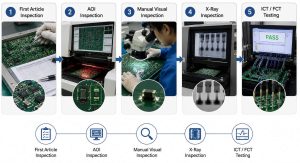
Common checks may include visual inspection, automated optical inspection, electrical test for bare boards, X-ray for hidden solder joints when needed, dimensional checks, and customer-defined functional testing. If functional testing is required, provide the test method, fixture needs, firmware, pass/fail limits, connector access, and safety precautions.

How to Compare Industrial PCB Manufacturing Suppliers

Compare suppliers by their ability to prevent production risk, not only by the lowest unit price. A suitable supplier should ask clarifying questions, flag missing data, explain manufacturing constraints, and document quote assumptions clearly.

  • Can the supplier review Gerber or ODB++ files before production?
  • Can they explain material, finish, copper, and stackup tradeoffs?
  • Can they support both bare board fabrication and assembly when needed?
  • Can they discuss inspection and testing based on the actual board risk?
  • Do they provide clear communication when a requirement needs engineering confirmation?
  • Do they avoid unsupported promises about lead time, certification, or yield?

What Determines Industrial PCB Manufacturing Cost?

Industrial PCB cost is shaped by board complexity, material choice, copper, finish, testing, assembly requirements, quantity, and how complete the RFQ package is. A cheap first quote can become expensive when missing assumptions are corrected later.

Cost factor Why it changes price How to reduce quote uncertainty
Layer count and stackup More layers and controlled builds need more process control. Provide stackup expectations and impedance notes early.
Material and copper Special materials and heavier copper affect sourcing and processing. State material targets, copper weight, and thermal needs.
Surface finish Finish affects assembly, shelf life, pad flatness, and cost. Choose based on component pitch and product needs.
Testing More inspection or functional checks add setup and labor. Define the exact pass/fail criteria and test method.
Assembly and sourcing BOM availability and assembly method affect schedule and price. Send BOM, CPL, approved alternates, and sourcing rules.

Files to Prepare for an Industrial PCB RFQ

A complete RFQ package lets the supplier quote the real project instead of quoting a partial guess. The more industrial risk your board carries, the more important it is to include the build notes and test expectations with the design files.

  • Gerber or ODB++ fabrication data
  • Drill files and board outline drawing
  • Stackup, material, copper, finish, and thickness notes
  • Controlled impedance requirements if applicable
  • BOM, CPL, assembly drawing, and polarity notes for PCBA
  • Quantity, prototype or production stage, and target delivery window
  • Inspection, electrical test, functional test, packaging, and labeling requirements

If you prefer to prepare an online quote package first, the PCB manufacturer online guide explains how buyers can organize the same information before contacting a supplier.

Common Industrial PCB Manufacturing Risks

The most common risks are incomplete files, unclear operating conditions, weak DFM review, BOM uncertainty, unverified special processes, and vague testing requirements. These risks usually appear as quote revisions, production holds, rework, or field issues.

Do not hide uncertainty in short notes. If a requirement is not final, label it as a target and ask the supplier to confirm feasibility. If a component may change, define who approves substitutions. If a board has thermal or vibration exposure, explain the real use case instead of assuming the supplier will infer it from the layout.

Frequently Asked Questions About Industrial PCB Manufacturing

Is industrial PCB manufacturing different from standard PCB fabrication?

Yes. The fabrication steps may look similar, but industrial projects usually need more attention to operating environment, DFM, repeatability, material choices, current load, inspection, and long-term reliability.

Can one supplier handle both PCB manufacturing and assembly?

Yes, when the supplier supports both fabrication and PCBA. A combined path can reduce handoff problems because Gerber, BOM, CPL, assembly notes, and testing requirements can be reviewed together.

What should I send for an industrial PCB quote?

Send Gerber or ODB++, drill files, stackup notes, material and finish requirements, quantity, target schedule, and any testing or packaging requirements. For assembly, also send BOM, CPL, and assembly drawings.

Should I choose the cheapest industrial PCB supplier?

Not automatically. Low price is useful only when the quote includes the real material, process, inspection, assembly, and testing requirements. Compare assumptions before comparing unit price.

Final RFQ Recommendation

Before placing an industrial PCB manufacturing order, prepare the files and risk notes that let the supplier review the project as a real production build. A strong RFQ package should include Gerber or ODB++, drill data, stackup, material, copper, finish, BOM, CPL, drawings, quantity, testing requirements, packaging notes, and target delivery timing.

For an engineering review or quotation, send your Gerber or ODB++ files, BOM, CPL, mechanical drawings, quantity, material expectations, surface finish, test requirements, and target lead time to sales@bestpcbs.com. The Best Technology / bestpcbs team can review the manufacturing path, confirm what needs project-specific checking, and help you prepare the next industrial PCB build without relying on hidden assumptions.

You may also like

PCB Design for Manufacturability Checklist Before Fabrication
Wednesday, July 15th, 2026

PCB design for manufacturability means checking a PCB layout against real fabrication and assembly constraints before the files are released for build. A useful DFM review catches file gaps, layout risks, material questions, assembly conflicts, and test problems early, when they are still easy to fix.

Use DFM before sending Gerber or ODB++ files for quotation, not after the first production problem appears. The goal is simple: help the board move from CAD data to PCB fabrication and PCBA with fewer engineering questions, fewer price changes, and fewer avoidable delays.

PCB design for manufacturability checklist with PCB layout Gerber review and inspection tools
PCB DFM works best when layout, stackup, drill, solder mask, assembly, and test details are reviewed before the files are released to manufacturing.

What PCB Design for Manufacturability Means

PCB design for manufacturability is the practice of designing a circuit board so it can be fabricated, assembled, inspected, and tested reliably by the chosen manufacturing process.

DFM is not only a software report. It is a practical engineering check between design intent and factory reality. The same schematic can be routed in a way that is easy to build or in a way that creates tight spacing, unclear drill data, soldering problems, poor test access, or repeated questions during quotation.

For buyers, DFM is a risk-control step. It helps decide whether the current file package is ready for a quote, prototype, pilot run, or production release. If the project also includes assembly, read DFM together with the PCB manufacturing and assembly guide so bare-board and PCBA risks are reviewed together.

When to Run a DFM Review

Run a DFM review before quotation, before prototype release, before production release, and whenever the board changes material, layer count, package density, or assembly method.

The best time is after layout is mature enough to export manufacturing data, but before purchase orders, panel plans, component commitments, or production schedules become fixed. At that point, the team can still adjust traces, vias, mask openings, component spacing, test pads, or drawings without turning every change into schedule pressure.

Project stage DFM focus Why it matters
Early prototype File completeness, obvious layout errors, package fit Prevents first-build rework and missing-file delays
Pilot build Repeatability, assembly access, test coverage Finds issues before the design is treated as stable
Production Yield risk, sourcing consistency, inspection method Reduces hidden cost and schedule surprises

Gerber, ODB++, Drill and Drawing Checks

The first DFM gate is file completeness, because unclear manufacturing data creates quote delays before anyone can evaluate the real board.

  • Confirm that all copper, solder mask, paste, silkscreen, outline, drill, and mechanical layers are exported.
  • Check whether the Gerber or ODB++ package matches the fabrication drawing and revision name.
  • Verify NC drill files, plated and non-plated holes, slots, cutouts, countersinks, and controlled-depth notes.
  • Remove old notes from previous revisions so the supplier does not quote against conflicting requirements.
  • Include a clear drawing when board outline, tolerances, impedance, panelization, or special processes matter.

If the same supplier will build and assemble the board, include BOM and CPL data early instead of sending bare-board files first and assembly files later.

Board Outline, Stackup and Material Checks

Board outline, stackup, thickness, material, copper, and impedance notes should be checked before release because they affect both manufacturability and quotation accuracy.

A design that looks correct in CAD may still create manufacturing questions if the outline is not closed, slots are not clearly defined, the stackup is missing, or the material is stated too loosely. For FR4, high Tg, RF, HDI, metal core, ceramic, flex, or rigid-flex work, the selected material route should be confirmed with the manufacturer instead of assumed from a generic rule.

For material-family context, BestPCBs product pages such as FR4 printed circuit boards and HDI PCB can be useful internal references, but exact limits should still be confirmed against the live project files.

Trace, Spacing, Via and Annular Ring Checks

Trace, spacing, via, drill, and annular ring rules should be checked against the intended process route, not copied from a generic internet table.

The safe rule is to design with margin. Very tight features may be possible on one process route and poor value on another. Before release, check whether the smallest trace, smallest gap, via type, drill-to-copper clearance, via-to-pad relationship, and board-edge clearance are appropriate for the supplier and the build quantity.

Item to check What can go wrong DFM action
Fine traces and spacing Yield loss, etching variation, re-quote Confirm rules before layout release
Small drills and vias Fabrication route changes or reliability questions Check drill table and annular ring margin
Vias near pads Solder wicking or assembly defects Review via-in-pad, tenting, filling, or spacing plan
Copper near board edge Routing damage or exposed copper Keep edge clearance consistent with the fabrication route

Copper, Solder Mask, Silkscreen and Surface Finish Checks

Copper weight, solder mask clearance, silkscreen placement, and surface finish should be checked together because they affect fabrication quality and assembly reliability.

DFM review should catch mask slivers, exposed copper, legend on pads, unclear polarity marks, and surface finish choices that do not match the assembly or storage requirement. The right finish depends on solderability, shelf life, pad design, component type, and project use, so it should be specified clearly in the RFQ instead of left as an assumption.

If cost is part of the decision, use the custom PCB cost guide together with the DFM checklist. Cost changes often come from the same details that make a design harder to build.

PCB Assembly DFM Checks

Assembly DFM checks whether the board can be populated, soldered, inspected, repaired, and tested without avoidable process risk.

For PCBA, bare-board manufacturability is only half of the review. Component footprint accuracy, part rotation, polarity marks, spacing around connectors, thermal relief, paste openings, BGA escape routing, tall-part clearance, and panel handling all matter. A board can pass fabrication review and still create assembly trouble.

  • Match BOM manufacturer part numbers to footprints and package data.
  • Check CPL or pick-and-place coordinates, rotation, side, and reference designators.
  • Make polarity, pin 1, connector direction, and LED orientation visible and unambiguous.
  • Review component spacing for soldering, inspection, rework, and enclosure fit.
  • Confirm whether special parts require hand soldering, selective soldering, fixtures, or extra inspection.

When the build includes assembly, the PCBA and PCB assembly service page is the natural service reference.

Test Point, Inspection and Quality Planning

DFM should include test and inspection planning because boards that cannot be inspected or tested efficiently carry higher production risk.

Ask how the board will be checked after fabrication and after assembly. Bare boards may need electrical testing. Assembled boards may need AOI, X-ray for hidden joints, functional test, fixture access, programming, or visual inspection. Test points should be accessible, labeled where needed, and compatible with the intended fixture or manual test method.

For capability context, the PCB test equipment page can support discussions about inspection and test expectations.

Cost and Lead-Time Risks Found by DFM

DFM often reduces cost and lead-time risk by finding manufacturability issues before they force a re-quote, redesign, material change, or assembly hold.

DFM issue Likely business impact How to reduce it
Missing drill or drawing data Quote delay Send complete manufacturing files first
Tight process features Higher cost or different route Confirm limits before final routing
BOM or CPL mismatch Assembly hold Review BOM, CPL, polarity, and footprint data together
Unclear testing need Late cost addition State electrical, AOI, X-ray, functional, or fixture needs early

DFM Checklist Before Releasing Files

A practical PCB DFM checklist should cover fabrication data, mechanical intent, assembly data, test requirements, and quotation scope before files are sent.

  • Gerber or ODB++ package includes every required layer and matches the revision.
  • NC drill, slots, plated/non-plated holes, cutouts, and board outline are clear.
  • Stackup, thickness, material, copper, impedance, finish, mask, and legend requirements are stated.
  • Smallest trace, spacing, drill, annular ring, and edge clearance are reasonable for the intended process route.
  • BOM, CPL, assembly drawing, polarity notes, approved substitutes, and special handling notes are complete.
  • Test requirements, inspection expectations, delivery target, quantity, and packaging needs are stated.

What to Send for a PCB DFM Review

For a useful PCB DFM review, send the same package you expect the manufacturer to quote and build, not only a screenshot or incomplete Gerber export.

For bare PCB fabrication, send Gerber or ODB++, NC drill, fabrication drawing, stackup, material preference, copper, finish, tolerance notes, quantity, and target delivery. For assembly, add BOM, CPL, assembly drawing, polarity notes, component alternatives, programming needs, and test plan.

If component sourcing is included, make sourcing expectations explicit. The component sourcing service page is a useful reference when the DFM review also needs BOM availability and substitute approval.

How to Work With a PCB Manufacturer on DFM Feedback

DFM feedback is most useful when the buyer and manufacturer agree which issues are mandatory fixes, which are recommendations, and which are acceptable project risks.

Do not treat every DFM comment as criticism of the design. Some comments protect yield, some clarify quotation scope, and some prevent assembly mistakes. Ask for the reason behind each major issue, then update the CAD source, exported files, fabrication drawing, BOM, or CPL so the approved change is visible in the next release package.

If your project is an early engineering build, the prototype PCB assembly page gives more context for prototype and small-batch review.

Common PCB DFM Mistakes

Common PCB DFM mistakes include incomplete files, unclear drawings, tight layout features without process confirmation, poor assembly markings, and missing test access.

Mistake Why it matters Better practice
Only Gerbers are sent for PCBA Assembly scope cannot be reviewed Send BOM, CPL, assembly drawing, and test notes
Old notes stay on drawings Supplier may quote the wrong requirement Clean revision notes before release
Polarity is unclear Assembly error risk increases Mark pin 1, diode, LED, capacitor, and connector orientation clearly
No test strategy is stated Late inspection or fixture cost may appear Define electrical, AOI, X-ray, or functional test needs early

Frequently Asked Questions About PCB Design for Manufacturability

What is PCB design for manufacturability?

PCB design for manufacturability is the process of checking a board layout, files, materials, assembly data, and test requirements against the way the board will actually be fabricated and assembled.

Is DFM only needed for complex PCBs?

No. Complex HDI, RF, flex, rigid-flex, or dense PCBA projects need deeper DFM, but even simple boards benefit from checking files, drill data, outline, polarity, and test requirements before quotation.

Can DFM reduce PCB cost?

DFM can reduce avoidable cost by finding problems that would otherwise cause re-quotes, fabrication questions, assembly holds, rework, or special process changes. It does not guarantee the lowest price; it helps make the quote more realistic.

What is the difference between DFM and DFA?

DFM focuses on whether the PCB can be manufactured reliably. DFA, or design for assembly, focuses on whether components can be mounted, soldered, inspected, and tested efficiently. PCBA projects need both.

Final Recommendation Before PCB Release

Before releasing a PCB for build, run one final DFM pass on the manufacturing files, assembly files, test requirements, and quotation assumptions.

If you want BestPCBs to review your design before fabrication or assembly, send Gerber or ODB++ files, NC drill files, stackup, fabrication drawing, BOM, CPL, quantity, material, surface finish, testing requirements, and target lead time through the contact page or email sales@bestpcbs.com. The clearer the file package is, the faster the team can confirm manufacturability, assembly scope, sourcing risks, and quotation details.

You may also like

LED PCB Manufacturer for Lighting and Power Electronics
Wednesday, July 15th, 2026
LED PCB manufacturer thermal inspection

An LED PCB manufacturer builds circuit boards that carry LEDs, manage heat, support reliable solder joints, and fit the mechanical and optical design of the final lighting product. For buyers, the main decision is not simply whether a supplier can make a PCB. The decision is whether the supplier can review thermal needs, substrate choice, copper design, LED placement, driver connections, assembly risk, testing, and RFQ files before production starts.

This guide is written for lighting engineers, purchasing teams, and product developers comparing LED PCB manufacturers for prototypes, pilot builds, and production. It focuses on commercial sourcing decisions: material, heat path, assembly, quality control, cost, and the files needed for a useful quote.

LED PCB Manufacturer Selection at a Glance

A good LED PCB manufacturer should help match board material, heat dissipation path, LED placement, assembly method, and inspection scope to the lighting application. LED boards are often more thermally sensitive than ordinary signal boards because light output, color stability, solder joint life, and product safety can all be affected by heat.

Buyer decision What to confirm Why it matters
Substrate FR-4, aluminum, copper, ceramic, or direct thermal path design Controls heat transfer, cost, weight, and manufacturability
Thermal path LED pad design, dielectric, copper, metal core, heat sink interface Affects LED life, brightness stability, and field reliability
Assembly LED package, polarity, driver parts, connectors, soldering method Reduces placement errors and solder defects
Testing Visual, AOI, polarity, illumination, electrical and thermal checks Finds issues before boards reach final products

When You Need an LED PCB Manufacturer Instead of a General PCB Supplier

You need an LED PCB manufacturer when heat, brightness, LED placement, mechanical fit, or assembly reliability are central to the project. A general PCB supplier may fabricate a board correctly from Gerber files, but LED products often need deeper review of heat path, component polarity, substrate choice, and how the board will be mounted into a fixture or power module.

Projects such as high-power lighting, automotive lighting modules, signage, industrial lamps, grow lights, UV LED systems, and compact consumer lighting need a supplier that can read the PCB files together with the LED package data, driver circuit, housing constraints, and expected operating conditions.

LED PCB Materials: FR-4, Aluminum, Copper, Ceramic and DTP Options

LED PCB material selection should follow the thermal and mechanical requirements of the product, not only the lowest board price. FR-4 may be acceptable for low-power indicator boards or lower thermal stress designs. Metal core PCB, copper core PCB, ceramic PCB, or direct thermal path structures may be considered when heat density is higher.

Bestpcbs has relevant product references for metal core PCB, SinkPAD-style thermal paths, ceramic PCB, and PCBA service. Exact material limits and construction options should be confirmed from the project files and capability tables before quoting. The safe RFQ approach is to share LED power, board outline, mounting surface, target temperature conditions, and thermal interface expectations early.

Thermal Design Questions to Answer Before RFQ

Thermal design questions should be answered before quote approval because heat problems are expensive to fix after LED placement and fixture design are locked. Even a well-fabricated board can fail if the heat path from LED junction to board, heat sink, housing, and ambient environment is not considered.

  • What is the LED package and power level?
  • Is the board mounted to a heat sink, housing, or metal frame?
  • Does the design need aluminum, copper, ceramic, or direct thermal path construction?
  • Are there thermal vias, exposed pads, or special copper areas?
  • Will the buyer provide thermal simulation, test conditions, or acceptance criteria?

Copper, Dielectric, Board Thickness and Surface Finish Choices

Copper, dielectric, board thickness, and surface finish choices affect both thermal behavior and manufacturing cost. For LED products, board thickness may be tied to mechanical fit, copper may be tied to current and heat spreading, and surface finish may affect solderability and storage conditions.

Do not assume all LED boards require the same build. A decorative LED board, a high-current lighting module, a compact driver board, and a high-power thermal board may need different substrate and assembly planning. The RFQ should state current, LED density, operating environment, finish preference, board thickness target, and mounting constraints.

LED PCB Assembly: LEDs, Drivers, Connectors and Polarity

LED PCB assembly requires careful handling of LED polarity, package orientation, driver components, connectors, and heat-sensitive placement details. A correct bare board is not enough if the assembled board has rotated LEDs, weak solder joints, or inconsistent brightness caused by component or process issues.

For assembly projects, provide BOM, CPL, assembly drawing, polarity notes, LED binning requirements if any, connector direction, and test expectations. If component sourcing support is needed, the component sourcing service is relevant for BOM availability, approved alternates, and supply risk review.

DFM Review for LED PCB Manufacturing

DFM review for LED PCB manufacturing checks whether the board can be fabricated, assembled, inspected, and mounted without avoidable production risk. This review should happen before production, not after defects appear.

Typical checks include LED pad size, solder mask clearance, copper balance, thermal pad design, mechanical holes, panelization, board outline, silkscreen clarity, polarity marking, connector placement, heat sink interface, and test point access. If the board also needs assembly, the review should connect Gerber, BOM, CPL, and assembly drawing data.

Testing and Inspection for LED PCB Projects

LED PCB testing should match the actual product risk, including electrical function, polarity, solder quality, visual appearance, and thermal behavior where required. Not every project needs every test, but the buyer should define what must be checked before shipment.

Possible checks include bare-board electrical testing, AOI, visual inspection, polarity verification, lighting function, driver output, current draw, and project-specific thermal checks. For assembled boards, the PCBA service path is relevant because assembly quality and board quality must be controlled together.

What Drives LED PCB Manufacturing Cost?

LED PCB cost is driven by thermal structure, material, copper, surface finish, assembly complexity, component sourcing, testing, and quantity. A low-power FR-4 LED indicator board and a metal-core high-power lighting module should not be priced or evaluated the same way.

Cost factor Impact on quote
Substrate FR-4, aluminum, copper, ceramic, and DTP structures follow different process routes.
Thermal design Thermal vias, metal cores, copper areas, and heat sink interface can add review and processing needs.
LED package and quantity Package size, polarity, and density affect assembly time and inspection risk.
BOM sourcing LED bins, drivers, connectors, and approved alternates can change price and schedule.
Testing Lighting, electrical, programming, or thermal checks add process time.

For a broader pricing view, compare this LED-specific checklist with the custom PCB cost guide.

Prototype, Pilot and Production LED PCB Planning

LED PCB prototypes should validate thermal and assembly assumptions before the buyer commits to production tooling, BOM purchasing, or fixture integration. Early prototypes help find LED spacing, brightness, driver, connector, and heat path issues while the design can still be changed.

For pilot and production, confirm whether the BOM is stable, whether LED binning matters, whether test fixtures are needed, and whether the same board build can be repeated. For engineering-stage builds, the prototype PCB assembly page is a useful internal reference.

How to Compare LED PCB Manufacturers

Compare LED PCB manufacturers by their ability to review thermal design, material choice, assembly data, sourcing risk, and testing requirements, not only by the first quoted unit price. A supplier that ignores heat and polarity can look inexpensive until the first failed build.

  • Can the supplier discuss LED substrate options and thermal path decisions?
  • Can they review Gerber, BOM, CPL, assembly drawing, and test needs together?
  • Do they ask about LED power, mounting, heat sink, operating environment, and brightness requirements?
  • Can they support both PCB fabrication and LED PCB assembly if needed?
  • Do they explain cost drivers instead of giving only a flat price?

Common LED PCB Sourcing Risks

Common LED PCB sourcing risks include weak thermal assumptions, missing polarity notes, unclear LED binning, wrong substitutions, and incomplete test requirements. These risks are easier to prevent before production than to repair after boards are assembled.

  • Thermal mismatch: substrate or heat path does not match LED power and fixture design.
  • Polarity error: LED orientation is unclear in CPL or assembly drawings.
  • BOM ambiguity: LED bins, drivers, connectors, or alternates are not approved.
  • Mechanical conflict: board holes, outline, or heat sink interface do not fit the final product.
  • Testing gap: brightness, current, function, or temperature checks are not defined.

RFQ Checklist for LED PCB Manufacturing

An LED PCB RFQ should include board files, LED and driver details, thermal requirements, assembly data, quantity, and inspection expectations. The more specific the RFQ, the fewer assumptions the supplier must make.

  • Gerber or ODB++ files and drill data
  • Board material, thickness, copper, finish, and thermal path notes
  • LED package, power, density, binning or brightness requirements if applicable
  • BOM with manufacturer part numbers and approved alternates
  • CPL / pick-and-place file and assembly drawing
  • Mounting, heat sink, housing, or mechanical constraints
  • Quantity for prototype, pilot, and production
  • Electrical, lighting, polarity, functional, or thermal test requirements

Frequently Asked Questions

What is an LED PCB?

An LED PCB is a printed circuit board designed to mount LEDs and related components while supporting electrical connection, heat transfer, mechanical fit, and product reliability. The board may use FR-4, metal core, ceramic, or other construction depending on power and thermal needs.

Is aluminum PCB always required for LED lighting?

No. Aluminum PCB is common for many lighting applications, but not every LED board requires it. Low-power designs may use FR-4, while higher heat-density designs may need aluminum, copper, ceramic, or direct thermal path structures.

Can one supplier handle LED PCB fabrication and assembly?

Yes, if the supplier can review the bare-board files, BOM, CPL, LED polarity, assembly drawing, and testing requirements together. This is often useful when the project has thermal and assembly risks.

What files are needed for an LED PCB quote?

Send Gerber or ODB++ files, drill files, material and thermal notes, BOM, CPL, assembly drawing, quantity, test requirements, and any mechanical or heat sink constraints.

What causes LED PCB quote differences between suppliers?

Quotes can differ because suppliers make different assumptions about substrate, copper, surface finish, LED package, component sourcing, assembly method, inspection, test scope, and production quantity.

Send an LED PCB Manufacturing RFQ

If you need LED PCB manufacturing or LED PCB assembly support, send your Gerber or ODB++ files, BOM, CPL, LED package details, quantity, material notes, thermal requirements, surface finish, testing requirements, and target delivery plan to the Best Technology / bestpcbs engineering team at sales@bestpcbs.com. The team can review the project for board build, heat path, sourcing, assembly, inspection, and quote preparation before production starts.

You may also like

PCB Manufacturing and Assembly for Prototype and Production
Wednesday, July 15th, 2026
PCB manufacturing and assembly production review

PCB manufacturing and assembly means building the bare circuit board, sourcing or preparing the components, mounting those components, and checking the finished PCBA before shipment. For buyers, the main question is not only whether a supplier can fabricate a PCB or assemble components. The real question is whether the supplier can review the files, catch manufacturability risks, manage BOM and CPL details, and deliver a board that can move into prototype, low-volume, or production use without avoidable rework.

This guide is written for engineers, hardware teams, and purchasing teams comparing PCB and PCBA suppliers. It explains what to prepare before requesting a quote, what affects cost and lead time, and which supplier checks matter before you release a design for manufacturing.

PCB Manufacturing and Assembly at a Glance

A complete PCB manufacturing and assembly workflow turns design files into finished PCBAs through fabrication, component preparation, assembly, inspection, testing, and shipment. The scope can be simple, such as a two-layer prototype with common SMT parts, or complex, such as a multilayer board with controlled impedance, fine-pitch packages, selective through-hole assembly, special material, and project-specific test requirements.

Stage What the supplier checks Buyer risk if missed
PCB fabrication Gerber or ODB++, stackup, drill files, copper, finish, solder mask, panel needs Wrong board build, poor fit, impedance risk, delayed production
Component preparation BOM, approved part numbers, alternates, package match, supply status Shortages, wrong substitutions, unexpected cost changes
PCB assembly CPL, polarity, package orientation, SMT/THT/BGA requirements, assembly drawing Placement errors, soldering defects, rework, failed bring-up
Inspection and testing AOI, X-ray where needed, visual checks, functional or customer-defined tests Hidden defects shipped to the buyer

When a Combined PCB and PCBA Supplier Makes Sense

A combined supplier is useful when the board design, component sourcing, assembly process, and delivery plan need to be reviewed as one connected project. This is especially important when the PCB layout affects component placement, when BOM availability affects the schedule, or when assembly test requirements should influence panelization and process planning.

Separate fabrication and assembly suppliers can work well for mature designs, but they create more handoff points. A combined path reduces the number of separate conversations around Gerber data, BOM questions, CPL corrections, material changes, soldering constraints, and final inspection criteria. Bestpcbs buyers can use the PCBA and PCB assembly service page as the service reference while using this article as the RFQ preparation checklist.

PCB Fabrication vs PCB Assembly: What Buyers Actually Receive

PCB fabrication produces the bare board, while PCB assembly mounts and solders electronic components onto that board to create a functional PCBA. Buyers often search both terms together because the final deliverable is not only a green board with copper traces. It is a board that can be powered, tested, integrated, and used in a product.

Fabrication decisions include material, layer count, copper weight, hole requirements, solder mask, surface finish, outline, and panelization. Assembly decisions include component packages, placement coordinates, soldering method, polarity markings, inspection method, and test coverage. If either side is treated as a separate afterthought, the finished board can become more expensive or slower to approve.

Files Needed Before a PCB Manufacturing and Assembly Quote

A reliable quote needs design files for the PCB, component data for the BOM, placement data for assembly, and clear instructions for testing and delivery. Missing files do not only slow the quote. They can also hide cost drivers that appear later, after the buyer thinks the project is already approved.

File or input Why it matters
Gerber or ODB++ Defines copper layers, solder mask, silkscreen, outline, and fabrication data.
Drill file Defines plated and non-plated holes, vias, and mechanical drill requirements.
Stackup or build notes Clarifies layer count, material expectations, copper, thickness, and impedance needs.
BOM Lists part numbers, quantities, approved alternates, and sourcing constraints.
CPL / pick-and-place file Provides component coordinates, rotation, and placement side.
Assembly drawing Clarifies polarity, special placement notes, connectors, and through-hole details.
Test requirements Defines what must be inspected or functionally checked before shipment.

If you want to upload files online, the PCB manufacturer online RFQ guide explains how to prepare the same package before sending it to an engineering team.

DFM, DFA, BOM and CPL Review Before Production

DFM and DFA review reduces the chance that a design looks correct in CAD but creates problems during fabrication, placement, soldering, or inspection. A supplier should not treat Gerber, BOM, and CPL files as separate documents. The files describe the same product from different angles, so mismatches should be found before production starts.

Important review points include footprint-to-BOM consistency, package orientation, polarity marks, solder mask clearances, via and pad decisions, panel edges, connector placement, component height concerns, and test point access. For assemblies, BOM and CPL review can be just as important as the bare board review because a wrong package or rotated part can stop a prototype even when the PCB itself is well fabricated.

PCB Materials, Board Types and Build Requirements to Confirm

Material and build requirements should be confirmed before quoting because they affect fabrication process, cost, risk, and assembly planning. Common decisions include FR-4 grade, high Tg material, Rogers or other high-frequency material, metal-core construction, ceramic substrates, board thickness, copper weight, surface finish, and controlled impedance.

Best Technology / bestpcbs maintains process capability references for standard PCB, MCPCB, ceramic PCB, FPC, and rigid-flex topics. Exact limits must be confirmed against the design files and the original capability tables before being written into a quote. In public content, the safer buyer rule is simple: provide the target material, layer count, board thickness, copper, finish, impedance need, operating environment, and expected quantity early so the supplier can confirm the build path instead of guessing.

SMT, Through-Hole, BGA and Mixed Assembly Choices

Assembly method depends on the component package mix, mechanical strength needs, inspection access, and production volume. SMT is common for compact, high-density electronics, through-hole assembly is often used for stronger mechanical connections or connectors, and BGA assembly requires careful footprint, paste, placement, and inspection planning.

Many real projects use mixed assembly. A board may combine fine-pitch ICs, connectors, power parts, LEDs, sensors, test pads, and manual soldering steps. When this happens, the quote should identify which side is assembled, whether there are through-hole or selective soldering steps, whether X-ray is needed for hidden joints, and whether any components require special handling.

Component Sourcing and Substitution Risk

Component sourcing can decide whether a PCB assembly project stays on schedule or becomes blocked by shortages, substitutions, and unexpected price changes. A BOM should not be treated as a static shopping list. It should be checked for lifecycle status, package match, minimum order issues, alternates, and approval rules.

If the supplier is expected to source parts, define whether substitutions are allowed and who approves them. A low quote can become expensive if it relies on weak sourcing assumptions. For projects where sourcing support is needed, the component sourcing service is a relevant internal reference for BOM and supply-chain discussions.

Testing and Quality Control Before Shipment

Quality control should be defined before production, because inspection after assembly cannot fix every design or sourcing decision made earlier. Buyers should ask what inspection steps apply to their board type, package mix, and risk level.

Typical checks may include bare-board electrical testing, solder paste and placement review, AOI, visual inspection, X-ray for hidden solder joints where appropriate, and functional testing when the buyer provides the test method, firmware, fixture, or acceptance criteria. The goal is not to add every possible test to every order. The goal is to match inspection depth to product risk, component package, quantity, and end-use expectations.

What Drives PCB Manufacturing and Assembly Cost?

Cost is driven by board complexity, component risk, assembly difficulty, testing scope, and quantity, not by size alone. A small board with fine-pitch parts and difficult sourcing can cost more than a larger but simpler assembly.

Cost factor Why it changes pricing
Layer count and stackup More layers and controlled structures add fabrication steps and review time.
Material and surface finish Special materials or finishes can change process route and procurement cost.
Drill, via, and copper requirements Dense holes, small vias, or heavier copper can affect fabrication difficulty.
BOM availability Shortages, alternates, and minimum buys can dominate assembly cost.
Package mix BGA, fine-pitch, through-hole, and mixed assembly affect placement and inspection.
Testing scope Functional testing, fixtures, programming, or special inspection add time and cost.

For a deeper pricing breakdown, use the custom PCB cost guide together with the BOM and assembly checks in this article.

Prototype, Low-Volume and Production Planning

Prototype, low-volume, and production PCB assembly should not be quoted the same way because each stage has a different risk profile. Prototype work usually needs fast engineering feedback, low setup friction, and tolerance for design changes. Production work needs repeatability, sourcing stability, inspection planning, and clearer acceptance criteria.

For early builds, ask the supplier to flag file issues before building. For low-volume runs, confirm whether the BOM can be repeated. For production, confirm packaging, panelization, test coverage, change control, and how replacement parts will be approved. If your current project is an early engineering build, the prototype PCB assembly page is a useful next reference.

How to Compare PCB Manufacturing and Assembly Suppliers

A good supplier comparison looks at engineering review, communication, sourcing control, inspection, and RFQ clarity, not only the lowest unit price. A cheap quote that ignores missing CPL data, uncertain parts, or test requirements can create a more expensive delay later.

  • Can the supplier review both fabrication and assembly files before production?
  • Does the supplier ask useful questions about BOM, CPL, polarity, and testing?
  • Can they explain which cost factors are driven by board build and which are driven by BOM or assembly?
  • Do they support the project stage: prototype, low volume, or production?
  • Can they route you to a relevant manufacturing or PCBA capability page instead of giving only a generic quote?

For bare-board capability context, buyers can also review the PCB manufacturing information page before sending a full PCBA package.

Common Sourcing Risks and How to Avoid Them

The biggest sourcing risks usually come from incomplete files, unclear substitution rules, missing test criteria, and late design changes. These problems are avoidable if the RFQ package is treated as an engineering document, not just a price request.

  • Missing CPL: provide pick-and-place data with rotation and side information.
  • Unclear polarity: mark LEDs, diodes, IC pin 1, electrolytic capacitors, and connectors clearly.
  • Weak BOM: include manufacturer part numbers, approved alternates, DNI parts, and sourcing notes.
  • No test definition: state whether visual inspection, AOI, X-ray, programming, or functional testing is expected.
  • Late material changes: confirm board material, copper, finish, thickness, and impedance requirements early.

RFQ Checklist for PCB Manufacturing and Assembly

A strong RFQ gives the supplier enough information to check manufacturability, sourcing, assembly, inspection, and delivery before issuing a price. Use this checklist before sending files.

  • Gerber or ODB++ files
  • Drill files and board outline
  • Stackup, material, copper, thickness, finish, and impedance notes
  • BOM with manufacturer part numbers and approved alternates
  • CPL / pick-and-place file
  • Assembly drawing and polarity notes
  • Quantity for prototype, pilot, and production stages
  • Testing, programming, inspection, packaging, and target delivery requirements

Frequently Asked Questions

What is the difference between PCB manufacturing and PCB assembly?

PCB manufacturing builds the bare circuit board from design data. PCB assembly mounts and solders components onto that board to create a PCBA. Buyers often need both steps together when they want one supplier to review fabrication files, BOM, CPL, assembly drawings, inspection, and final shipment.

Can I request PCB fabrication first and assembly later?

Yes, but it is better to consider assembly during fabrication planning. Component placement, test access, panelization, soldering method, and connector location can affect how easily the board can be assembled later.

What files are most important for a PCBA quote?

Gerber or ODB++ files, drill data, BOM, CPL, assembly drawings, quantity, material notes, surface finish, and testing requirements are the core inputs. The more complete the package, the fewer assumptions the supplier must make.

Should the supplier source components or should I provide them?

Either model can work. Supplier sourcing can reduce buyer workload, but the BOM must define approved parts and substitution rules. Consigned parts can be useful when buyers already control inventory or approved vendor lists.

Why do PCB assembly quotes change after review?

Quotes can change when the supplier finds BOM shortages, missing files, package mismatches, special inspection needs, design risks, or unclear test requirements. A complete RFQ reduces late changes.

Send a PCB Manufacturing and Assembly RFQ

If you need PCB manufacturing and assembly support, send your Gerber or ODB++ files, BOM, CPL, quantity, material notes, surface finish, assembly drawing, testing requirements, and target delivery plan to sales@bestpcbs.com. The team can review the package for fabrication, component sourcing, assembly, inspection, and quote preparation, then identify the questions that should be solved before production starts.

You may also like

PCB Manufacturing Energy Consumption and Embodied Energy
Wednesday, July 15th, 2026

PCB manufacturing energy consumption is the electricity, heat, process energy, material energy, and indirect supply-chain impact needed to turn laminate, copper, chemistry, tooling, and design data into a finished printed circuit board. For most buyers, the useful question is not a single universal kWh number. It is which board decisions, fabrication steps, supplier controls, and quote details can reduce unnecessary energy, scrap, rework, and embodied carbon without weakening reliability.

PCB manufacturing energy consumption in a fabrication process

Public PCB life-cycle and decarbonization research generally points in the same direction: board impact depends on materials, fabrication energy, chemicals, yield loss, transport, assembly, use phase, and end-of-life treatment. Those inputs vary sharply by stackup and process. A simple two-layer FR-4 board, a high-layer-count HDI board, a metal-core thermal board, and an automotive ceramic substrate do not carry the same manufacturing burden.

What PCB Manufacturing Energy Consumption Means

PCB manufacturing energy consumption means the energy used directly in fabrication plus the upstream energy already embedded in materials such as copper foil, laminate, prepreg, solder mask, surface finish chemistry, and packaging. In practical sourcing, it is better to treat this as a decision map than as a fixed number.

A buyer can influence energy-related impact before the order reaches the factory. Layer count, board size, copper weight, via structure, impedance tolerance, surface finish, acceptance criteria, and panel utilization all affect how many process steps the board needs. A supplier can influence the same outcome through process control, first-pass yield, waste handling, equipment efficiency, and transparent data collection.

Where Energy and Carbon Impact Enter the PCB Life Cycle

Energy enters the PCB life cycle through raw materials, fabrication, assembly, transport, product use, rework, and disposal or recycling. A quote that only compares unit price can miss several of these drivers.

Life-cycle stage Typical energy or carbon driver Buyer check
Material production Copper, glass fiber, resin, ceramic, aluminum or specialty laminate production Ask whether the requested material is necessary for the electrical, thermal, or mechanical requirement.
PCB fabrication Imaging, etching, lamination, drilling, plating, solder mask, surface finish, routing and testing Confirm which process steps are driven by the stackup and tolerance choices.
Assembly Stencil printing, placement, reflow, inspection, cleaning, selective soldering, test fixtures Separate bare-board and PCBA requirements in the RFQ.
Yield and rework Scrap panels, rejected boards, rework loops and repeated testing Provide complete files and request DFM review before production release.
Logistics Shipment mode, partial shipments, urgent reorders and packaging Plan quantities and approval steps early enough to avoid emergency freight.

Which PCB Design Choices Usually Affect Energy Use

The design choices most likely to change manufacturing energy are layer count, board area, copper thickness, via structure, controlled impedance, surface finish, and tolerance tightness. Each one can add process complexity when it goes beyond what the design actually needs.

Layer count is often the first lever. Extra layers may be necessary for routing density, EMI control, power integrity, or controlled impedance, but they also add lamination, imaging, inspection, and material demand. Board size and panel utilization matter as well. A shape that wastes panel area can increase scrap even when the finished board is small.

Copper thickness affects etching and plating. Via structures affect drilling, desmear, plating, filling, capping, and inspection steps. Surface finish should match assembly and storage needs rather than habit. If the project only needs standard solderability, an expensive or process-heavy finish may not be justified.

How Fabrication Steps Influence Energy Consumption

Fabrication energy is distributed across repeated wet processing, lamination, drilling, plating, baking, inspection, routing, and testing steps. The more times a board must pass through those steps, the more important process discipline becomes.

For example, a multilayer board may require inner-layer imaging and etching before layup, then lamination, drilling, copper plating, outer-layer imaging, solder mask, surface finish, profiling, electrical test, and final inspection. An HDI design can add laser drilling, microvia plating, sequential lamination, via filling, and tighter inspection. These process choices may be technically correct, but they should be tied to a real electrical or reliability need.

For a plain-language explanation of how stackup and process complexity interact, see our guide to multilayer PCB manufacturing.

Why Yield, Scrap, and Rework Matter

Yield is one of the most overlooked energy variables because every scrapped board carries the material and process energy already spent on it. Lower yield can turn a technically efficient process into a wasteful one.

Many yield problems start before fabrication: missing drill files, unclear stackup notes, ambiguous copper requirements, insufficient annular ring, unsupported solder mask slivers, unrealistic impedance tolerances, and mismatch between BOM, CPL, and drawings for PCBA orders. A proper DFM review reduces the chance of re-running panels, remaking tooling, or holding production while questions are resolved.

For buyers comparing fabrication plus assembly scope, the distinction between a bare PCB and a fully assembled PCBA also matters. The article PCB vs PCBA explains where the manufacturing boundary changes.

How Materials and Layer Count Change Embodied Energy

Embodied energy changes when a board uses more material, harder-to-process material, tighter reliability requirements, or a stackup that needs extra lamination and inspection. A lightweight design is not automatically lower impact if it causes poor yield or field failure.

FR-4, high-Tg FR-4, low-loss RF laminate, metal-core materials, ceramic substrates, heavy copper, and rigid-flex constructions solve different engineering problems. The lower-impact choice is the material that satisfies the product requirement with the least avoidable complexity. For thermal products, that may mean using a metal-core or ceramic option only where the heat path demands it. For high-speed products, it may mean choosing a stable laminate and stackup early so the factory does not need repeated trial builds.

Cost and sustainability often meet in the same place: avoid over-specification, avoid unclear files, and avoid rework. Our custom PCB cost guide covers many of the same quote variables from a price perspective.

What Buyers Can Ask Before Requesting a PCB Quote

The best RFQ questions focus on data quality, process fit, yield protection, and whether the supplier can explain tradeoffs instead of making vague carbon claims. Most buyers do not need a perfect carbon model for every board; they need better decisions before production starts.

  • Can the supplier review stackup, material, copper weight, via type, tolerance and finish before quoting final production?
  • Which requested features are driving extra lamination, plating, drilling, testing or inspection steps?
  • Can panel utilization be improved without changing the finished board outline?
  • Are any tolerances tighter than the product actually needs?
  • Will the quote separate bare-board fabrication, assembly, testing, tooling, freight and rework risk?
  • Can the supplier flag file issues that may cause scrap before mass production?

How to Compare Suppliers Without Unverified Carbon Claims

Compare suppliers by the quality of their manufacturing data and engineering review, not by unsupported ?green PCB? marketing language. If a supplier gives a carbon or energy figure, ask what scope, boundary, method, and board assumptions it uses.

A useful comparison should state whether it covers material production, board fabrication, assembly, transport, use phase, and end-of-life. It should also clarify whether the data is plant-level, product-level, estimate-based, or supplier-reported. Without those boundaries, two numbers may look comparable while measuring different things.

For online sourcing workflows, the file package still matters. Our article on choosing a PCB manufacturer online lists the documents that help a supplier quote and review the board properly.

Practical Design Checks for Lower-Impact PCB Sourcing

The most practical way to lower unnecessary impact is to design for manufacturability, avoid avoidable complexity, and give the supplier enough information to build the board right the first time. The same habits usually reduce lead-time risk and cost.

  1. Confirm that layer count and stackup are needed for the signal, power, thermal, and mechanical requirements.
  2. Use the simplest via structure that still meets density and reliability needs.
  3. Choose copper weight based on current, thermal rise, and manufacturability, not guesswork.
  4. Match surface finish to assembly, storage, wire bonding, or contact requirements.
  5. Review panelization early when the board outline is unusual.
  6. Run DFM review before freezing production quantity.
  7. Separate prototype learning builds from production release builds.

If your project includes assembly or component sourcing, include BOM and placement files at the same time as Gerber or ODB++ data. The PCBA service page explains the broader manufacturing scope beyond bare-board fabrication.

FAQ About PCB Manufacturing Energy Consumption

These questions come up when engineering teams start connecting PCB sourcing with carbon, cost, and manufacturing reliability.

Is there one standard energy number for PCB manufacturing?

No. Energy depends on board size, layer count, material, copper weight, via structure, surface finish, process route, yield, test scope, and factory energy mix. A single number without board assumptions is not useful for sourcing.

Does fewer layers always mean lower embodied energy?

Usually fewer layers reduce material and process complexity, but not always. If forcing fewer layers causes poor routing, EMI problems, rework, or field failure, the lower layer count may create more waste over the product life.

Can DFM review reduce PCB energy consumption?

DFM review can reduce avoidable scrap, repeated tooling, rework, and production holds. It does not magically make a board low-carbon, but it helps prevent waste caused by unclear or difficult-to-build designs.

Should buyers ask PCB suppliers for carbon data?

Yes, when the project requires sustainability reporting. Ask for the boundary and method behind the data. A plant-level or estimate-based value should not be treated the same as a product-specific life-cycle calculation.

Final RFQ Checklist for Energy-Aware PCB Projects

For an energy-aware PCB quote, send the same files needed for a reliable build, plus any sustainability reporting requirements you must meet. The goal is practical clarity, not green decoration.

  • Gerber or ODB++ files.
  • Stackup request, material preference, copper weight, impedance and thickness targets.
  • Surface finish, solder mask, silkscreen and special process requirements.
  • Quantity, prototype or production intent, and target lead time.
  • BOM, CPL, assembly drawing and test requirements if PCBA is included.
  • Any carbon, lifecycle, material declaration, RoHS/REACH or supplier reporting requirement.
  • Known design risks where DFM review is needed before release.

If you want a practical review before committing to production, send your Gerber or ODB++ files, BOM, CPL, quantity, material choice, surface finish, testing requirements, target lead time, and any sustainability reporting requirement to sales@bestpcbs.com. Our team can review the manufacturing route, flag avoidable complexity, and help you prepare a quote package that supports both reliability and lower-waste sourcing.

You may also like

PCB Manufacturer Online: Quote Files, DFM Checks and Ordering Risks
Wednesday, July 15th, 2026

A PCB manufacturer online can help you move from design files to a price request faster, but the safest quote still depends on complete manufacturing data, clear assembly scope, and a DFM review before release. Uploading Gerbers is only the start. Buyers also need drill files, stackup notes, quantity, material, surface finish, testing requirements, and, for PCBA, BOM and CPL data.

Use online PCB manufacturing as a fast RFQ channel, not as a substitute for engineering judgment. If the board has tight tolerances, impedance, special materials, heavy copper, HDI, flex sections, controlled testing, or component sourcing risk, ask the supplier to review the files before you treat the first price as final.

PCB manufacturer online quote preparation with Gerber files BOM and circuit boards
Online PCB quotes work best when the Gerber, drill, stackup, BOM, CPL, quantity, material, finish, and test requirements are ready before upload.

What Does a PCB Manufacturer Online Actually Provide?

A PCB manufacturer online usually provides a digital way to submit PCB files, select specifications, request pricing, communicate requirements, and start fabrication or assembly review.

For simple prototype boards, that may be enough to get a quick estimate. For production or engineering-critical work, the online path should still connect to real manufacturing review. The important question is not only whether a website accepts files. The useful question is whether the supplier can catch missing information before the board reaches fabrication.

Online function What it helps with What still needs review
File submission Gerber, drill, ODB++, drawings, BOM, CPL Missing layers, naming errors, stackup mismatch
Quote request Quantity, board size, copper, finish, delivery target Special process, material availability, test scope
Order communication Questions, engineering notes, delivery details DFM exceptions, substitutions, approval records

Online PCB Manufacturer vs Engineering-Led RFQ

An online PCB quote is best for speed, while an engineering-led RFQ is better when the board has design, process, assembly, sourcing, or reliability risk.

Many searches for a PCB manufacturer online are driven by convenience. Buyers want a price without several email rounds. That is reasonable for a simple two-layer prototype. It becomes risky when the board has impedance control, fine-pitch parts, unusual materials, via-in-pad, tight mechanical fit, thermal stress, or production testing needs.

BestPCBs provides an online enquiry path for PCB and PCBA projects. Treat it as a structured RFQ entry point: send complete files, then let the engineering and sales team confirm manufacturability, assembly scope, and quotation details.

Files You Need Before Requesting an Online PCB Quote

The fastest online PCB quote is the one that starts with a complete file package, because missing files create engineering questions and price changes later.

  • Gerber or ODB++ fabrication files with all copper, solder mask, paste, legend, outline, and mechanical layers.
  • NC drill files, drill map, slot notes, and plated/non-plated hole definitions.
  • Stackup, finished thickness, copper weight, material preference, impedance notes, and tolerance requirements.
  • Surface finish, solder mask color, silkscreen color, panelization preference, and testing requirements.
  • For assembly: BOM, CPL or pick-and-place file, assembly drawing, polarity notes, approved alternates, and functional test plan.

If you are not sure whether you need bare PCB fabrication or complete assembly, compare the sourcing path in this PCB vs PCBA guide before you request pricing.

What Instant PCB Quotes Can Calculate Well

Instant PCB quote tools are useful for standard specifications that can be priced from clear inputs such as size, layers, quantity, thickness, copper, solder mask, finish, and delivery target.

These tools can give a reasonable starting point when the design fits normal fabrication rules. They are especially useful for early budget comparisons, prototype planning, and checking how quantity or lead time changes the price.

Input Usually easy to price online Needs confirmation when
Board size and quantity Panel area and batch cost Outline is irregular or panelization is constrained
Layer count and thickness Standard stackups Impedance or special dielectric is required
Surface finish Common finish options Special reliability or shelf-life requirement exists
Assembly quantity Placement count and basic labor BOM availability or substitutes are uncertain

What Online PCB Quote Tools Often Miss

Online quote tools often miss the engineering details that change manufacturability, yield, component sourcing, test method, or final delivery risk.

A price form may not understand whether a trace runs too close to the board edge, whether a connector area needs mechanical support, whether a component is obsolete, or whether a test point is reachable after assembly. These are not small details. They can decide whether the first build ships on time or turns into a rework discussion.

For a deeper look at price drivers, use the custom PCB cost guide together with your online quote comparison.

How to Compare PCB Manufacturer Online Options

Compare online PCB manufacturers by engineering response, file review, material clarity, assembly support, testing options, communication, and delivery reliability, not price alone.

  • Does the supplier review Gerber, drill, stackup, and drawing data before release?
  • Can they quote both bare PCB and PCBA manufacturing when the project needs assembly?
  • Do they ask for test requirements instead of assuming only basic electrical test?
  • Can they explain price changes when a design moves from prototype to repeat production?
  • Do they provide a clear communication path if a file, material, or BOM issue appears?

Bare PCB, PCBA, and Turnkey Quote Differences

Bare PCB quotes cover the board only; PCBA quotes add component mounting; turnkey quotes also include component sourcing, assembly, inspection, and sometimes functional testing.

Confusing these scopes is a common online ordering mistake. A bare board price may look low because it excludes components, stencil, placement, inspection, and test. A PCBA quote may change after BOM review if parts are unavailable, package data is unclear, or approved alternates are missing.

If the project needs parts procurement, include sourcing expectations early and review the component sourcing service path before you compare suppliers.

DFM Checks Before You Upload Gerbers

A quick DFM check before upload reduces quote delays because the manufacturer receives files that are easier to review and price accurately.

  • Confirm board outline, slots, cutouts, and mechanical dimensions match the drawing.
  • Check minimum trace, spacing, annular ring, drill size, and solder mask clearance against the intended supplier route.
  • Verify layer order, copper weights, impedance notes, and controlled-depth or special drill instructions.
  • For assembly, check polarity marks, part rotation, footprint fit, test points, and connector orientation.
  • Remove conflicting notes from old revisions before sending the RFQ package.

The older PCB manufacturing process page can help buyers understand why each fabrication step needs clean input data.

Cost Factors That Change After Engineering Review

PCB cost can change after engineering review when the original online inputs miss material choice, tolerance, special process, assembly complexity, component availability, testing, or schedule pressure.

Cost driver Why it changes after review How to reduce surprise
Material Selected material may not match electrical, thermal, or availability needs Send material preference and acceptable alternatives
Drill and copper rules Tight features may require a different process route Confirm design rules before final layout release
Assembly Fine-pitch parts, BGAs, odd shapes, or hand operations change labor and inspection Send BOM, CPL, drawings, and photos if available
Testing Functional test, fixture needs, or special inspection may not be included State test requirements in the first RFQ

Lead Time, Shipping, and Communication Risks

Online ordering can shorten the quote cycle, but lead time still depends on complete files, material availability, engineering questions, production load, testing scope, and shipping route.

Do not compare two online quotes only by the number shown beside delivery. Ask whether the time starts after payment, after file approval, after engineering questions are cleared, or after components arrive. For assembled boards, component sourcing can easily become the pacing item.

Prototype assemblies often need a different planning rhythm from production builds; the prototype PCB assembly page is a useful reference when the goal is a fast engineering build.

Red Flags Before Placing an Online PCB Order

Red flags include a quote that ignores missing files, accepts unclear stackups, does not ask about test requirements, hides assembly exclusions, or cannot explain what happens when DFM issues appear.

  • The supplier gives a final-looking price from screenshots instead of manufacturing files.
  • The quote form has no place for drawings, tolerance notes, testing, or assembly requirements.
  • The BOM review does not mention lifecycle, package, substitute, or sourcing risk.
  • Delivery timing is advertised but not tied to engineering approval or component arrival.
  • Support cannot explain what happens if the Gerber and drawing disagree.

When to Ask for Manual Engineering Review

Ask for manual engineering review when the PCB has controlled impedance, HDI, heavy copper, flex or rigid-flex areas, high temperature, RF behavior, fine-pitch assembly, special testing, or production reliability requirements.

Manual review does not slow a serious project down; it prevents hidden problems from reaching production. A good supplier should be willing to review your files, explain unclear points, and confirm the quote scope before release.

Frequently Asked Questions About Online PCB Manufacturers

Can I get a reliable PCB quote online without talking to an engineer?

For simple prototypes, sometimes yes. For production, assembly, controlled impedance, unusual materials, or tight mechanical requirements, engineering review is safer before you approve the price.

What files should I upload for a PCB manufacturer online?

Upload Gerber or ODB++, drill files, stackup notes, material and finish requirements, quantity, test requirements, and, for PCBA, BOM, CPL, assembly drawings, and approved alternates.

Why does an online PCB price change after review?

The first price may not include missing process details, special materials, assembly difficulty, component sourcing risk, test fixtures, or delivery constraints.

Is the cheapest online PCB manufacturer always the best choice?

No. The lowest price is useful only when the quote scope, files, testing, delivery terms, and quality expectations are the same.

Final RFQ Checklist

Before choosing a PCB manufacturer online, prepare the complete file package and ask for review of the items that can affect quality, cost, and schedule.

  • Gerber or ODB++, NC drill, board outline, stackup, material, copper, finish, and quantity.
  • BOM, CPL, assembly drawing, polarity notes, approved alternates, and test plan for PCBA.
  • Target lead time, delivery address, packaging needs, and any reliability or inspection requirement.
  • Clear note if the quote is for prototype, pilot run, repeat production, or long-term sourcing.

If you want BestPCBs to review your project before quotation, send your Gerber or ODB++ files, drill files, stackup, BOM, CPL, quantity, material, surface finish, test requirements, and target delivery date through the online enquiry page or email sales@bestpcbs.com. The more complete the file package is, the faster the team can confirm manufacturability, assembly scope, sourcing risks, and quote details.

You may also like

Custom PCB Cost: Quote Factors, Quantity and Cost-Saving Checks
Monday, July 13th, 2026

The cost of a custom PCB is determined by the complete manufacturing specification, not by board dimensions alone. Layer count, finished size, panel utilization, laminate, copper weight, hole and via structure, surface finish, test scope, quantity, and requested lead time all change the quote.

For a useful price comparison, send the same released data package to each supplier and make sure every quote covers the same revision, quantity, quality requirements, testing, tooling, and delivery terms. A low total is not a saving if a missing item returns later as an extra charge or a reliability problem.

Engineer reviewing different custom PCB designs and quotation documents
Custom PCB pricing starts with the released board data, manufacturing specification, quantity, test scope, and delivery requirement.

What Does a Custom PCB Quote Actually Include?

A custom PCB quote should define the boards being fabricated, the manufacturing setup, the verification included, and the commercial terms used to calculate the total. Buyers should not compare only the unit price because suppliers may place tooling, electrical test, certificates, freight, or expedite charges on separate lines.

Quote area What to confirm Why it changes the comparison
Board fabrication Revision, dimensions, layer count, material, copper, finish, quantity Confirms that every supplier priced the same physical board
Engineering and tooling Data review, phototools, routing programs, test setup, special fixtures Fixed charges can dominate prototype and small-batch totals
Inspection and test Electrical test, impedance coupons, reports, microsection or special acceptance records Different verification scopes can make two prices look comparable when they are not
Commercial terms Lead time, freight, taxes, packaging, payment terms, quote validity The delivered cost may differ from the fabrication subtotal

Before approving a purchase order, ask whether the price is for bare boards only. Assembly, components, stencils, programming, functional test, cables, enclosures, and box build belong to a PCBA or turnkey scope unless the quotation states otherwise.

Which Inputs Change Custom PCB Cost the Most?

The largest cost changes usually come from the board’s layer structure, material area, production quantity, feature difficulty, and verification requirements. The dominant factor varies by design: panel yield can control a large simple board, while sequential lamination or controlled-depth drilling can control an HDI design.

Input Typical cost effect Best buyer check
Finished size and array Changes laminate use and boards per production panel Confirm finished outline, edge features, and permitted panelization
Layer count and stackup Adds copper layers, prepreg/core, imaging, registration, and lamination work Release an approved stackup or performance requirements
Hole and via structure Changes drilling, plating, filling, capping, and lamination sequence Identify through, blind, buried, microvia, back-drill, and filled-via requirements
Material and copper Changes raw material cost, process windows, and availability Specify exact grade when required; otherwise state the electrical and thermal need
Quantity Spreads fixed setup over more boards but increases total material Request the quantities you may genuinely purchase
Test and documentation Adds machine time, coupons, reports, fixtures, or destructive samples Define acceptance evidence before suppliers quote

These inputs interact. A smaller outline may lower material use, but very tight routing could require finer fabrication capability. A cheaper laminate may be unsuitable for high-speed, high-temperature, or RF performance. Cost review should therefore follow the board’s functional risks rather than a universal list of cuts.

How Do Board Area and Panel Utilization Affect Price?

Board area affects cost through laminate consumption and the number of usable circuits that fit on a production panel. A few millimeters added to one edge can sometimes reduce the boards-per-panel count, so price does not always change in a smooth line with area.

Irregular outlines, large cutouts, edge connectors, routing clearance, coupons, tooling rails, and spacing rules also affect panel yield. Ask the fabricator whether a small outline adjustment or a different delivery array would improve utilization without changing the enclosure, creepage distance, mechanical strength, or assembly process.

Engineer inspecting a twelve-up bare PCB production panel
Panel utilization changes material yield and can materially affect both prototype and production quotations.

Why Do Layer Count and Lamination Cycles Raise PCB Cost?

More layers require additional cores or copper foils, imaging steps, registration control, inspection, and lamination work. The increase is not simply the price of extra copper; the stackup creates more process stages and more opportunities for scrap if alignment or material flow is not controlled.

Blind and buried vias may require sequential lamination, which adds complete drilling, plating, imaging, and pressing cycles. Before removing layers to save money, confirm that routing density, reference planes, return paths, impedance control, isolation, and power distribution still meet the design need. For conventional constructions, review available FR4 printed circuit board options with the fabricator instead of naming a costly specialty material by habit.

When Do Materials and Copper Weight Change the Quote?

Materials change the quote when their purchase price, stocking status, panel format, processing behavior, or required certification differs from a standard production laminate. High-Tg FR4, low-loss RF laminates, polyimide, metal-core structures, ceramic substrates, and specified laminate brands should not be treated as interchangeable cost items.

Copper weight affects both raw material and processing. Heavier copper can require different etching allowances, wider conductor spacing, more resin to fill around copper features, and tighter control of the finished surface. Specify heavy copper only where current capacity, thermal behavior, mechanical strength, or an approved design standard requires it.

How Do Hole Size, Via Type, and Routing Density Affect Fabrication Cost?

Small holes, dense drilling, blind or buried vias, laser microvias, filled vias, capped vias, controlled-depth drilling, and back-drilling add cost because they require different equipment, more machine time, extra plating or filling, and additional inspection.

A design that moves from ordinary through vias to an HDI PCB structure should be quoted from the actual via map and stackup. The supplier needs to know which layers each via connects, whether microvias are stacked or staggered, whether via-in-pad is filled and capped, and whether any holes have finished-size or aspect-ratio constraints. A drill table that only lists diameters is not enough for a reliable HDI quote.

What Do Surface Finish and Solder Mask Choices Cost?

Surface finish changes the quote through chemistry, process control, coverage area, handling, shelf-life requirements, and local availability. HASL, lead-free HASL, ENIG, immersion silver, immersion tin, OSP, hard gold, and other finishes solve different solderability, flatness, wear, wire-bonding, or storage needs.

Solder mask color alone is often less important than the required dam width, registration, via treatment, thickness, and compatibility with the assembly process. Unusual colors, multiple mask operations, selective plating, carbon ink, peelable mask, edge plating, or hard-gold fingers should be clearly marked in fabrication notes and drawings so the supplier does not price a standard board and revise it later.

How Does Quantity Change Tooling and Unit Cost?

Quantity changes unit cost because engineering review, CAM preparation, imaging setup, routing programs, and some test preparation are fixed or semi-fixed for a released revision. A prototype batch carries those costs across few boards; a larger repeat order spreads them across more usable circuits.

The lowest unit price is not always the lowest project cost. Ordering too many boards before electrical, mechanical, assembly, and field risks are verified can turn a favorable unit price into obsolete inventory. A practical comparison often requests prototype, pilot, and expected production quantities on the same data package, then checks which charges repeat after a revision.

How Do Electrical Testing and Quality Requirements Affect Price?

Test scope affects price through machine time, fixture cost, sample consumption, engineering review, and the records delivered with the order. Flying-probe testing is flexible for prototypes and changing designs, while fixture-based testing can become more efficient when stable volume justifies dedicated tooling.

Controlled-impedance coupons, test reports, microsections, solderability checks, ionic cleanliness requirements, thermal stress, first-article records, lot traceability, or customer-specific acceptance plans should be included in the RFQ. Do not remove a required test only to lower the quote; instead, identify which failure the test is intended to catch and whether a different verification method provides adequate evidence.

Flying-probe electrical testing of a bare multilayer PCB
Electrical-test method, coverage, reporting, and dedicated fixtures should be aligned with revision stability and order volume.

How Do Lead Time and Expedite Requests Change Pricing?

A shorter lead time can change pricing when the order requires reserved capacity, off-schedule material purchasing, overtime, faster external processing, split shipments, or priority logistics. The effect depends on the board technology and material availability, not only the requested number of days.

Ask suppliers to separate fabrication time from material procurement, engineering questions, approval holds, transit, and customs time. A nominal quick-turn quote is not comparable if one supplier starts the clock after every engineering question is closed while another includes data review. Freeze the revision and answer DFM questions promptly if schedule is the real priority.

What Is the Difference Between Bare PCB Cost and PCBA Cost?

Bare PCB cost covers fabrication of the unpopulated circuit board; PCBA cost adds component procurement, stencil and programming setup, SMT or through-hole assembly, inspection, cleaning, programming, functional test, rework allowances, packaging, and sometimes box build.

Component availability can dominate a PCBA total even when the bare board is simple. If you need an assembled prototype, request a separate view of board fabrication, components, assembly labor/setup, and test. The prototype PCB assembly scope should state BOM revision, approved alternatives, placement data, assembly drawings, programming files, and test responsibility. For supply-risk work, define the expected component sourcing controls rather than comparing only BOM totals.

Where Can PCB Cost Cutting Create Reliability Risk?

Cost cutting becomes false economy when it removes a requirement that controls an actual electrical, thermal, mechanical, assembly, or environmental risk. Common examples include changing laminate without checking Tg or electrical behavior, reducing copper without reviewing current and temperature rise, shrinking annular rings, relaxing test coverage, or accepting unapproved component substitutions.

  • Do not remove reference planes only to reduce layer count if return paths and EMC depend on them.
  • Do not substitute a surface finish without checking component pitch, storage, multiple reflow cycles, contact wear, and downstream bonding.
  • Do not loosen impedance requirements unless simulations or system margins support the change.
  • Do not compare suppliers with different inspection, traceability, or test obligations.
  • Do not treat unapproved laminate or copper substitutions as harmless purchasing changes.

How Can You Reduce Custom PCB Cost Without Weakening the Board?

The safest cost reductions remove unnecessary complexity while preserving the functions and acceptance evidence the product needs. Start with a DFM and value-engineering review before the layout and sourcing choices are frozen.

  1. Confirm that finished dimensions and arrays use material efficiently.
  2. Use standard stackups, materials, copper weights, finishes, and drill sizes where performance permits.
  3. Remove blind vias, via filling, back-drilling, controlled depth, or sequential lamination only when the design can function without them.
  4. Separate mandatory tolerances from drawing defaults and cosmetic preferences.
  5. Plan prototype, pilot, and production quantities instead of buying volume before validation.
  6. Freeze released data and consolidate documentation so suppliers do not price uncertainty.
  7. Ask which one or two specification changes would produce the largest saving, then review the engineering consequence of each.

A supplier familiar with the full custom PCB board fabrication flow can usually identify cost drivers more accurately from Gerber or ODB++, drill data, stackup, and fabrication notes than from a short parameter list.

How Should You Compare Two Custom PCB Quotes?

Compare quotes line by line against one controlled RFQ package. Normalize the revision, quantity, delivery destination, test scope, tooling treatment, commercial terms, and exceptions before deciding that one supplier is cheaper.

Comparison check Questions to ask
Technical match Did both suppliers quote the same stackup, material, copper, finish, via treatment, tolerances, and special processes?
Quantity and yield Are shipped quantity, overrun/underrun rules, panel delivery, and scrap assumptions clear?
Tooling Which setup charges repeat after reorder or data revision?
Test and evidence Are electrical test, impedance, reports, coupons, traceability, and acceptance records equivalent?
Schedule When does the lead-time clock start, and are material procurement and shipping included?
Exceptions Which requirements were excluded, changed, or left for engineering review?
Delivered total Are freight, packaging, payment fees, duties, and taxes treated consistently?

If a low quote omits a difficult requirement, ask for a corrected quotation instead of relying on a verbal promise. The purpose of quote comparison is to expose technical and commercial differences before production, not after a purchase order is placed.

What Files Are Needed for an Accurate Custom PCB Quote?

An accurate quote requires enough controlled information for the fabricator to identify every material, process, tolerance, inspection, and delivery obligation. Sending only Gerber files may leave the supplier guessing about the stackup, finished hole sizes, controlled impedance, special processes, and acceptance documentation.

  • Gerber, ODB++, or another agreed fabrication data set
  • NC drill files with plated and non-plated hole definitions
  • Fabrication drawing and released revision identifier
  • Approved stackup or electrical/material performance requirements
  • Board dimensions, outline, cutouts, edge details, and delivery-array requirements
  • Material grade, finished copper, board thickness, solder mask, legend, and surface finish
  • Controlled-impedance table and coupon/report requirements where applicable
  • Via filling, capping, back-drill, depth, edge plating, countersink, or other special-process notes
  • Inspection, electrical test, traceability, certificate, and acceptance requirements
  • Prototype, pilot, and production quantities with target delivery location and date

For a project-specific cost review, send the released fabrication package and quantity breaks to sales@bestpcbs.com. Ask the engineering team to identify assumptions, excluded items, and the largest safe cost-reduction opportunities before you compare the quotation.

Frequently Asked Questions

Can a PCB supplier give an accurate price from board dimensions alone?

No. Dimensions help estimate material area, but a usable quote also needs layer count, stackup, material, copper, drill and via data, surface finish, tolerances, test scope, quantity, and lead time. A dimension-only number should be treated as an early estimate, not a released production quotation.

Why is a prototype PCB more expensive per board?

Prototype orders spread CAM review, imaging, routing setup, test preparation, and other fixed work across few boards. The total may be manageable while the unit price appears high. Prototype pricing also reflects low panel utilization when the batch cannot be combined efficiently with other compatible work.

Does a larger order always reduce the total PCB cost?

No. A larger order usually reduces unit cost by spreading setup and improving production efficiency, but total spend rises with material and processing volume. Buying more before validating the revision can also create obsolete inventory, so quantity decisions should follow prototype and pilot evidence.

Is a two-layer PCB always cheaper than a four-layer PCB?

A conventional two-layer board is normally simpler to fabricate, but the complete design still matters. A forced two-layer layout may become larger, need difficult routing, create EMC problems, or require costly rework. Compare the total project consequence rather than layer count in isolation.

Does ENIG always cost more than HASL?

ENIG commonly has a higher process cost than standard HASL options, but the correct choice depends on pad flatness, component pitch, storage, soldering, contact, and bonding needs. Pricing and availability vary by supplier, so the RFQ should specify the required finish and acceptance standard.

Why do filled vias or via-in-pad increase cost?

Filled and capped vias require additional filling, curing, planarization, plating, and inspection. They may also interact with sequential lamination and microvia reliability. Use them where package escape, thermal transfer, or pad geometry requires them, not as an automatic default across the board.

What is NRE in a PCB quotation?

NRE means non-recurring engineering or setup cost. Depending on the supplier, it may cover CAM preparation, tooling, test fixtures, special programming, or other order-specific work. Ask which NRE items repeat after a reorder, quantity change, or data revision.

Can changing PCB color reduce the price?

Using a supplier’s standard solder mask and legend options may avoid special scheduling or material handling, but color is rarely the largest cost driver. Layer structure, panel yield, material, via technology, test scope, quantity, and lead time usually deserve attention first.

Should freight be included when comparing PCB suppliers?

Yes. Compare the delivered commercial scope, not only the fabrication subtotal. Confirm freight method, packaging, shipment splits, insurance, duties, taxes, and delivery destination. Two similar board prices can produce different landed costs and schedules.

How long should a custom PCB quote remain valid?

Quote validity depends on material pricing, availability, exchange rates, workload, and commercial policy. The supplier should state the validity period. Reconfirm price and lead time when the revision, quantity, material source, delivery date, or market conditions change.

Final Recommendation

Treat custom PCB pricing as an engineering comparison, not a single-number auction. Release one complete RFQ package, require suppliers to identify assumptions and exceptions, compare equivalent test and delivery scopes, and challenge the few design choices that create the largest cost without protecting product performance.

Request a Custom PCB Cost Review

If you are budgeting a custom PCB prototype or production order, send your Gerber or ODB++ data, drill files, fabrication drawing, stackup, quantity breaks, test requirements, and target delivery date to sales@bestpcbs.com and request a quotation. The Best Technology engineering team can review the package, clarify quote assumptions, and prepare a project-specific quotation without replacing required reliability controls with false savings.

You may also like

Custom PCB Design for Mining: Dust, Vibration and Power Checks
Monday, July 13th, 2026
Custom PCB design for mining equipment with rugged enclosure and connector harness

Custom PCB design for mining equipment should be reviewed around dust, moisture, vibration, protected power input, connector strain relief, thermal control, test points and production-ready RFQ files. A mining electronics board is not only a circuit layout. It is part of a rugged system that may sit near motors, pumps, sensors, conveyors, vehicles, lighting, chargers or communication devices where contamination, shock and repair access matter.

This guide is written for engineers and buyers preparing a custom PCB or PCBA for mining-related equipment. It focuses on practical design and manufacturing checks before fabrication or assembly. If the product will be used underground, near combustible dust, or in another regulated hazardous area, confirm the applicable equipment-level certification requirements with your compliance team. A PCB supplier can support design for reliability, traceability and production quality, but board fabrication alone does not certify the complete mining device.

What does custom PCB design for mining need to solve?

Mining PCB design needs to keep electrical performance stable while the board is exposed to dust, vibration, heat, moisture, long cable runs and maintenance stress. The exact risks depend on whether the board is used in a sensor node, motor controller, lighting module, communication gateway, battery system, display panel or test device.

For a simple monitoring module, the main issues may be enclosure fit, connector sealing and low-power reliability. For a power or drive-related board, the review moves toward copper weight, creepage and clearance, thermal paths and protection components. Compact control electronics may also need an HDI PCB if the enclosure is tight and the component density is high.

Mining design risk PCB or PCBA check Why it matters
Dust and moisture Enclosure interface, coating decision, connector sealing and cleaning process Contamination can create leakage paths, corrosion and intermittent faults
Vibration and shock Mounting holes, board support, connector retention and heavy component placement Loose connectors or cracked solder joints can stop equipment in the field
Power variation Input protection, grounding, copper width, fusing and transient protection Long cables and inductive loads can create voltage stress
Heat buildup Copper weight, thermal vias, enclosure contact and material selection Sealed boxes often have limited airflow
Maintenance Test points, labels in drawings, harness plan and replaceable modules Field teams need faults isolated quickly without damaging the board

Where are custom mining PCBs used?

Custom mining PCBs are common in control, sensing, communication, lighting, power conversion and equipment monitoring devices. A buyer should define the use case before asking for a quote, because a sensor interface board and a high-current control board need different materials, copper rules and test plans.

Typical examples include conveyor monitoring electronics, pump controllers, battery management devices, rugged displays, LED lighting modules, wireless gateways, environmental sensors and vehicle-mounted control units. Some designs use standard FR4 PCB construction. Others need heavier copper, higher Tg material, metal-backed structures, conformal coating, sealed box integration or full PCBA support.

How should dust, moisture and enclosure fit be handled?

The PCB should be designed together with the enclosure, gasket, connector system and cleaning/coating plan. Treating the board as a flat electrical drawing and the enclosure as a later mechanical decision often creates failures at cable entries, mounting bosses, edge clearance and service access.

Engineers reviewing a rugged mining equipment PCB with enclosure gasket and connector samples
Mining electronics should be reviewed as a board, enclosure, connector and testable assembly, not as a bare PCB only.

Before layout release, check the board outline against the enclosure drawing, connector keepout area, mounting-hole tolerance, coating keepout, service connector position and any pressure-equalization or sealing requirement. If conformal coating is planned, mark no-coat areas around connectors, switches, programming pads and test contacts. If potting is planned, confirm component height, thermal behavior and repair expectations before the production file is frozen.

What vibration checks matter before production?

Vibration risk is controlled by board support, connector retention, solder joint protection and heavy component placement. A mining PCB can pass an electrical review and still fail in the field if a large inductor, terminal block, relay, transformer, battery connector or harness load is not mechanically supported.

Use larger mounting margins around high-stress areas. Keep heavy parts away from unsupported board edges when possible. Add strain relief for harnesses instead of letting cable pull act directly on solder joints. For mixed SMT and through-hole designs, define whether wave soldering, selective soldering or hand operations are expected. If the design includes high-current terminals, compare the copper and spacing assumptions against a relevant design reference such as the Heavy Copper PCB Design Guide.

How should power input and heat be reviewed?

Power input review should cover voltage range, surge exposure, reverse polarity risk, grounding, heat flow and copper current capacity. Mining equipment often connects through long cables, battery systems, motors, relays, lighting modules or chargers. These conditions can put more stress on input circuits than a clean lab supply.

For early DFM, send the supplier the expected operating voltage, maximum current, copper weight, target temperature range, board thickness, surface finish and any thermal interface to the enclosure. Do not ask for only a bare board price if the real product needs heat-spreading, coated assembly, heavy connectors or functional testing. The quote should reflect the way the board will be used.

Design area Questions to answer before RFQ
Input power What voltage range, current load, fuse strategy and reverse-polarity protection are required?
Grounding How are chassis ground, signal ground and shield termination handled?
Thermal path Will heat leave through copper pours, vias, thermal pads, an enclosure wall or a heatsink?
Copper weight Are high-current traces sized for the real load and temperature rise target?
Protection Are surge, ESD and inductive switching risks reviewed at cable and connector interfaces?

Which materials and stackups fit mining electronics?

The material choice should follow the electrical load, enclosure temperature, vibration risk and required board density. FR4 is often suitable for control and sensor boards, but high-current, high-heat or compact assemblies may need different copper, laminate, via and thermal decisions.

For dense signal boards, HDI can reduce routing congestion and help fit a smaller rugged enclosure. For power boards, thicker copper, larger spacing and thermal planning may matter more than density. For LED lighting or heat-generating modules, metal-backed or direct thermal path designs may be considered. The right choice depends on the project files, not on a generic mining label.

How should assembly and sourcing be planned?

Mining PCBA planning should include component availability, substitute approval, coating or sealing steps, test fixture needs and final box-level handling. A bare PCB schedule does not describe the finished product if the order also needs SMT, through-hole assembly, wiring, enclosure fit or functional testing.

Before releasing the order, provide a controlled BOM, approved alternates, centroid file, assembly drawing, polarity notes, connector orientation, firmware loading requirement and test criteria. If long-life parts or industrial-grade components are required, discuss Component Sourcing early. If the supplier is expected to deliver a mounted board in a sealed housing, treat it as a Box Build Assembly discussion rather than a normal PCB-only purchase.

What test plan should be ready before release?

The test plan should prove the board can be built, inspected and checked consistently before it reaches the field. At minimum, define electrical test for bare boards, AOI or visual inspection for assembly, functional checks for powered boards and any project-specific connector, LED, sensor, relay or communication test.

Mining equipment PCB assembly under electrical test with rugged connector harness and sealed enclosure
Testing should be planned before production release, especially when cables, connectors, sealed boxes and field power inputs are involved.

Useful test points should be accessible after assembly, not hidden under large components or blocked by the enclosure. If the board has firmware, define how programming and verification are handled. If the product uses sensors, motors, relays or communication interfaces, list the pass/fail behavior in simple language. A supplier’s PCB test equipment capability should be part of the RFQ discussion when the board needs repeatable inspection instead of only continuity checks.

RFQ checklist for custom PCB design for mining

A useful RFQ package lets the supplier review reliability risks before quoting cost and lead time. Send the same controlled package to every supplier if you want to compare quotes fairly.

  1. Gerber files, drill files, netlist and controlled revision number.
  2. Board drawing with thickness, outline tolerance, mounting holes and connector keepouts.
  3. Stackup, copper weight, material preference and surface finish requirement.
  4. Expected operating voltage, current load, thermal concern and enclosure notes.
  5. BOM, approved substitutes, centroid file and assembly drawing if PCBA is included.
  6. Coating, potting, cleaning, labeling, packaging or box-build requirements.
  7. Test plan with required measurements, programming steps and pass/fail criteria.
  8. Compliance notes for the final equipment, especially if the use environment is regulated.

Supplier questions buyers should ask

The best supplier questions are specific enough to reveal whether the factory has reviewed the board as a mining electronics assembly, not just a generic PCB. Use the questions below before approving production.

  • Which part of this design creates the highest manufacturing risk?
  • Are the mounting holes, edge clearances and connector keepouts suitable for the enclosure?
  • Is the copper weight enough for the stated current and temperature target?
  • Do any components need adhesive, mechanical support or layout changes for vibration?
  • Which components have sourcing risk, and are substitutes already approved?
  • Can the test points still be reached after assembly or box build?
  • What should be changed before moving from prototype to production?

FAQ

What is custom PCB design for mining?

Custom PCB design for mining means designing a circuit board or PCBA for equipment used around mining operations, such as sensors, controllers, lighting, communication modules, power electronics or monitoring devices. The design must consider dust, vibration, moisture, power stress, enclosure fit, connectors, testing and production repeatability.

Does a mining PCB need a special material?

Not always. Many mining control or sensor boards can use FR4 when the electrical load and temperature are moderate. High-current, high-heat, compact or harsh-environment designs may need heavier copper, higher-grade laminate, HDI, metal-backed construction, coating or a different stackup. The material should follow the real design risk.

Can a PCB supplier certify mining equipment?

A PCB supplier can support reliable board fabrication, assembly, traceability, inspection and documentation. Certification for equipment used in regulated mining or hazardous environments is usually a system-level issue. Confirm ATEX, IECEx, MSHA or local requirements with qualified compliance specialists before production decisions.

What files are needed for a mining PCB quote?

Send Gerber files, drill files, board drawing, stackup, copper weight, surface finish, BOM, centroid file, assembly drawing, enclosure notes and test requirements. If the board will be coated, potted or installed in a sealed box, include those details in the first RFQ instead of adding them later.

What causes delays in mining PCB projects?

Common delays include unclear enclosure drawings, missing connector orientation, unapproved component substitutes, vague test criteria, incomplete power requirements and late coating or box-build decisions. A controlled RFQ package helps the supplier check manufacturability before committing to lead time.

Conclusion

Custom PCB design for mining should be treated as a rugged electronics project, not a normal board order with a different label. Start with the environment, enclosure, connectors, power input, heat path, component sourcing and test plan. Then ask the supplier to review the files for manufacturability before quote approval. That process gives the buyer a better chance of receiving a board that can be assembled, inspected and supported in real mining equipment.

You may also like

Custom Metal-Backed PCB Lead Times: Materials and Supplier Checks
Monday, July 13th, 2026
Metal-backed PCB lead time planning with aluminum core PCB samples and RFQ documents

Custom metal-backed PCB lead times depend on material availability, stackup complexity, copper or aluminum base selection, surface finish, routing profile, testing requirements and how complete the RFQ files are. A supplier can usually quote faster when the Gerber files, drill data, stackup, base metal requirement, thermal target, quantity, finish and assembly needs are clear before review. If any of those items are missing, the schedule often stalls before production even starts.

This guide is written for buyers and engineers comparing custom metal-backed PCB lead times between suppliers. It focuses on the practical checks that affect delivery risk for aluminum PCB, copper core PCB, MCPCB and direct thermal path boards, not generic promises about speed.

What affects custom metal-backed PCB lead times?

The biggest schedule drivers are material choice, thermal structure, fabrication process, assembly scope and review quality before release. Metal-backed boards are not always difficult, but they are less forgiving than a simple FR4 prototype because the base metal, dielectric layer and mechanical profile all affect thermal performance and manufacturability.

For a standard single-layer Metal Core PCB, the factory review usually starts with the aluminum or copper base, dielectric thermal conductivity, copper weight, solder mask, finish and outline method. For double-sided or multi-layer designs, the review becomes more detailed because plated holes, layer registration, insulation, flatness and heat path design must be checked together.

Lead time factorWhat the supplier checksWhy it can slow the schedule
Base metalAluminum, copper, iron alloy or direct thermal path structureNon-standard base thickness or copper base availability may need confirmation
Dielectric layerThermal conductivity, insulation strength and thicknessSpecial dielectric materials may require extra sourcing or DFM review
Copper weightTrace width, spacing, current load and etching controlHeavy copper changes etching, solder mask and inspection risk
Mechanical profileCNC routing, V-cut, milling, countersink or unusual shapeMetal substrates often need slower tool paths and tighter fixture planning
Assembly and testLED polarity, thermal pad contact, functional test and packagingPCBA adds component sourcing, SMT scheduling and quality checks

Which RFQ files should be ready before asking suppliers?

A complete RFQ package removes the most common waiting time: back-and-forth clarification. At minimum, prepare Gerber files, drill files, board drawing, stackup request, base material notes, copper weight, surface finish, solder mask color, quantity, target date and whether the order includes assembly.


Engineer reviewing metal-backed PCB samples, stackup drawing and production schedule before RFQ
Complete files help the supplier confirm material, stackup, routing and schedule before production release.

For boards with LEDs or power devices, include thermal assumptions instead of only sending the circuit image. The supplier needs to know whether the board is a general aluminum PCB, copper core PCB, SinkPAD Board, or another direct thermal path design. If the design needs a special heat path, the lead time should not be judged from a normal MCPCB quote.

  • Gerber and drill data with clear revision control.
  • Mechanical drawing with board thickness, outline tolerance and hole notes.
  • Stackup or construction requirement, including base metal and dielectric.
  • Copper weight, surface finish and solder mask requirement.
  • Assembly BOM, centroid file and polarity notes if PCBA is included.
  • Testing requirement, packaging method and any thermal validation request.

Which material choices change the schedule?

Material choices change lead time when they are outside the supplier’s normal stock, need tighter thermal control or require a different fabrication route. A basic aluminum substrate is usually easier to plan than a copper core board, a double-sided MCPCB or a multi-layer metal-backed build.

A double-sided MCPCB needs closer review than a single-sided board because the supplier must confirm insulation, drilling, plating, alignment and surface preparation through a metal base structure. High-current areas may also push the design toward heavier copper, larger spacing or local thermal relief. If the same design also needs SMT, conformal coating, box build or special packaging, the buyer should treat fabrication and assembly as one schedule instead of two separate dates.

When the material is the main risk, ask the supplier to confirm whether the base metal, dielectric and copper foil are stocked, reserved or still pending procurement. A fast quote is not the same thing as confirmed material availability.

How should suppliers review manufacturability before committing a date?

A reliable supplier should check the thermal structure, mechanical profile, copper design and test plan before promising a ship date. The best warning sign is not a long lead time; it is a very fast promise made before anyone has checked the metal substrate details.

For metal-backed PCB projects, DFM review should include conductor spacing, copper-to-edge distance, dielectric isolation, heat path, milling risk, solder mask coverage and finish compatibility. If assembly is included, the review should also include component availability through Component Sourcing, stencil design, polarity, thermal pad soldering and inspection method.

Ask the supplier to identify what is fixed and what is still conditional. A clear answer might say: material is available, outline needs CAM review, assembly components need two substitutes approved, and functional testing needs a fixture. That kind of detail is more useful than a one-line promise.

Where do testing and assembly fit into the lead time?

Testing and assembly should be scheduled before the order is released, not discovered after boards are fabricated. A bare board schedule only covers fabrication. A real project schedule may also include SMT, through-hole assembly, cleaning, AOI, electrical test, thermal contact checks, fixture setup and final packaging.

MCPCB production panels under probe testing before shipment
Electrical inspection, routing and final handling can affect the delivery date for metal-backed PCB panels.

If your order includes prototype PCB assembly, the supplier must align PCB fabrication, component arrival, SMT line time and quality checks. For production builds, test fixtures and packaging can matter just as much as board fabrication. Use the supplier’s PCB test equipment capability as a schedule discussion point, especially when the board drives LEDs, power modules, sensors or high-current loads.

Metal core PCB process footage can help buyers understand why material preparation, routing and inspection need schedule space.

Supplier checklist before placing the order

The safest order decision comes from confirming files, materials, DFM status, assembly scope and test requirements in writing. Use the checklist below before approving a custom metal-backed PCB lead time.

  1. Confirm the supplier has reviewed the latest Gerber, drill, drawing and stackup files.
  2. Ask whether the aluminum, copper or special dielectric material is in stock or needs procurement.
  3. Confirm the board type: standard MCPCB, copper core, double-sided MCPCB, SinkPAD or another thermal structure.
  4. Ask which process step is most likely to affect delivery: material, CAM, drilling, routing, finish, assembly or testing.
  5. Confirm whether component sourcing and substitutes are approved before SMT scheduling.
  6. Require a final delivery date after DFM review, not before the supplier has checked the files.
  7. Keep one controlled revision package so the quote, production order and inspection plan match.

For high-power or thermal products, also review related material guidance such as Metal Core PCB Material. Material choice is often where schedule, cost and reliability meet.

FAQ

How should buyers compare custom metal-backed PCB lead times between suppliers?

Compare suppliers after the same RFQ package has been reviewed. If one supplier quotes from a finished DFM review and another quotes from an email summary, the dates are not equal. Ask each supplier to state material availability, CAM status, assembly scope, testing needs and open questions.

Is an aluminum PCB always faster than a copper core PCB?

Not always, but a standard aluminum PCB is often easier to schedule when material is stocked and the design is simple. Copper core, direct thermal path and unusual mechanical profiles usually need more review because heat transfer, insulation and routing risks are higher.

What causes the most common RFQ delays?

Missing drawings, unclear base material, incomplete drill data, uncertain copper weight, unapproved component substitutes and vague testing requirements cause many delays. The supplier can quote faster when the buyer sends a controlled file set and answers technical questions before release.

Should assembly lead time be counted separately from PCB fabrication?

For planning, count it as part of the same project schedule. PCB fabrication, component sourcing, SMT scheduling, inspection and final testing affect the delivery date seen by the buyer. A bare board lead time is useful, but it does not describe a finished PCBA order.

When should I use SinkPAD or direct thermal path boards?

Use SinkPAD or another direct thermal path structure when heat must move from a component pad into the metal base more directly than a normal dielectric layer allows. The design should be reviewed early because this structure affects stackup, fabrication route and schedule.

Conclusion

Custom metal-backed PCB lead times are easiest to control when the RFQ is specific, the material path is confirmed and the supplier performs DFM before promising a date. Treat the schedule as an engineering decision: verify the stackup, base metal, thermal path, assembly scope and test plan first, then compare suppliers on confirmed delivery risk instead of headline speed.

You may also like