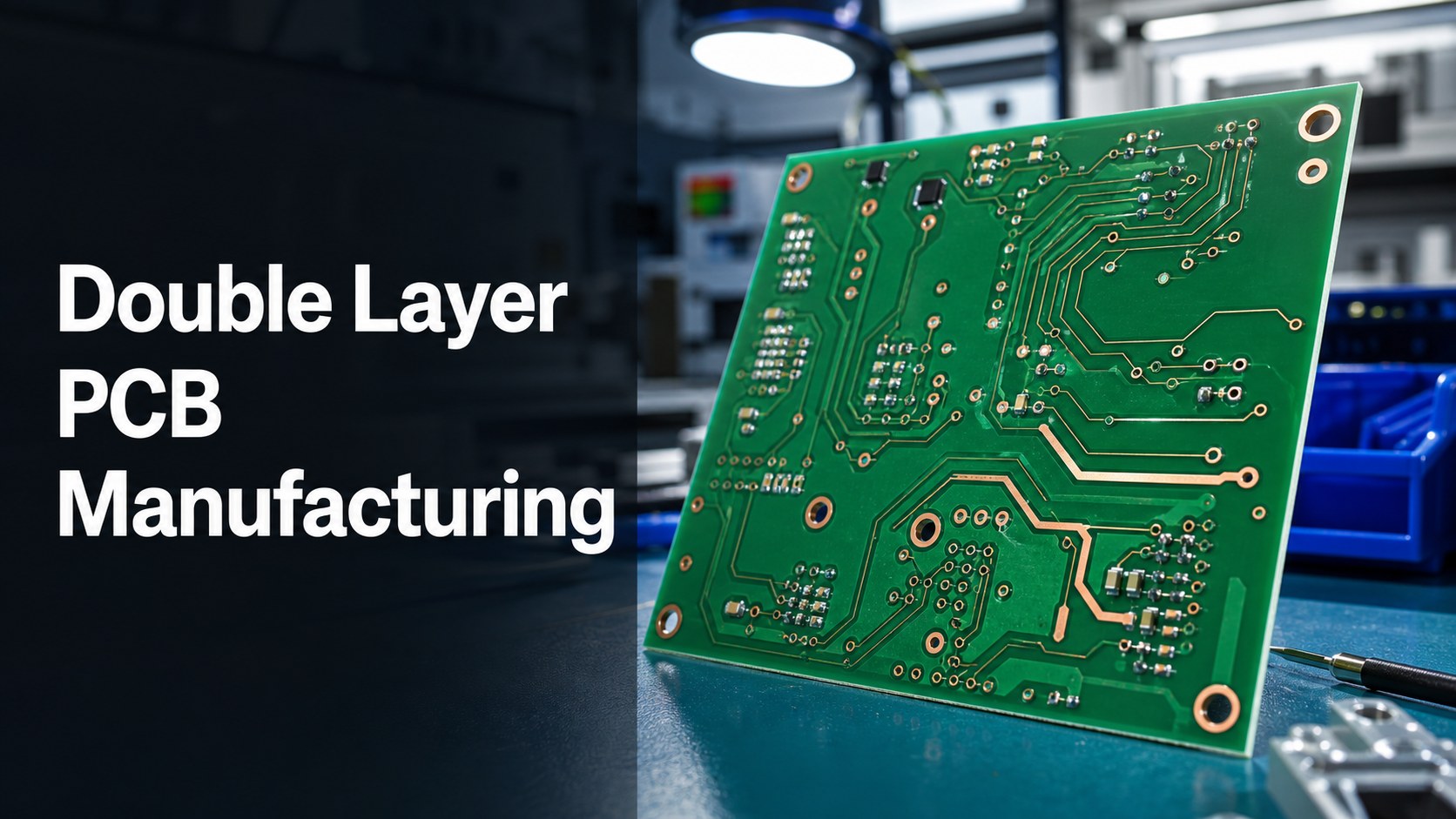
Double layer PCB manufacturing builds a printed circuit board with copper circuitry on both sides of an insulating core, connected by plated through holes. It is often the best choice when a single-sided board cannot route the circuit cleanly, but the project does not yet need the cost, stackup control or density of a multilayer PCB.
For buyers, the real decision is not only whether the board has two copper layers. The safer question is whether your manufacturer can review the Gerber data, copper weight, drill file, annular ring, solder mask, surface finish, test method and assembly needs before fabrication starts. That review is where many two-layer boards either become easy to build or quietly turn into delay, rework and cost.
Is your double layer PCB order getting stuck before production?
Many two-layer boards look simple on the purchase order, but the issues usually appear inside the fabrication files:
- Through-hole pads are too small for the drill tolerance, leaving weak annular rings after plating.
- Trace width and spacing are copied from a prototype tool without checking the finished copper weight.
- The stackup does not leave enough board thickness, copper balance or mechanical margin for the enclosure.
- Solder mask openings, bridges and silkscreen markings are not matched to the assembly process.
- The RFQ only asks for a unit price, so the supplier does not review test points, panelization or PCBA risk early enough.
EBest Circuit helps buyers turn a two-layer PCB file into a build-ready order.
- We review Gerber, drill, drawing and stackup details before production release.
- We check copper weight, hole plating, solder mask bridge, outline and finish choices against manufacturability.
- We support bare board fabrication and optional PCBA so layout, fabrication and assembly risks can be handled together.
- We help buyers normalize quotes by board thickness, finish, test method, panelization and order quantity instead of comparing unit price alone.
- We keep the project discussion practical: what can be built as standard, what needs confirmation, and what should be corrected before the order starts.
Double Layer PCB Manufacturing in One Practical Answer
Double layer PCB manufacturing is the process of making a board with top and bottom copper layers connected by plated through holes. It is used for control boards, power interfaces, LED drivers, sensor boards, industrial electronics, consumer products and many PCBA projects where routing on one side is not enough.
A two-layer PCB normally gives more routing freedom than a single-sided board, better grounding options, shorter jumper paths and easier component placement. Compared with multilayer PCB manufacturing, it usually keeps the stackup simpler and the cost easier to control.
When a Two-Layer PCB Is the Right Build
A two-layer PCB is right when the design needs routing on both sides but does not require controlled multilayer power planes or very high density. It is a common fit for moderate-density components, connectors on both sides, low-to-medium speed signals, simple power paths and production boards that need reliable plated vias.
If your board has dense BGA escape, strict impedance control, high-speed interfaces or multiple isolated power domains, a multilayer stackup may be safer. If the circuit is very simple and one side can route cleanly, a single-sided board may still be enough. The best choice comes from routing, copper, assembly and test requirements together.
What Buyers Need to Control Before Fabrication
The most important buyer controls are copper weight, minimum trace and spacing, hole size, annular ring, board thickness, finish and test coverage. These items decide whether a two-layer board can be produced as a standard order or needs engineering confirmation.
| RFQ Item | Why It Matters | What to Send |
|---|---|---|
| Copper weight | Affects trace width, heat rise, etching and price | Finished copper requirement for each side |
| Drill file | Controls plated through holes and component fit | NC drill file plus finished hole notes |
| Board thickness | Affects rigidity, connector fit and V-cut planning | Drawing or stackup note |
| Surface finish | Affects soldering, storage and contact reliability | OSP, HASL, ENIG or other finish choice |
| Testing | Confirms opens, shorts and production reliability | Electrical test and special inspection needs |
How EBest Circuit Reviews a Two-Layer PCB Order
EBest Circuit reviews a two-layer PCB order by connecting the drawing, Gerber, drill data, copper, finish and assembly plan before quoting. This avoids a quote that looks attractive but misses the details that later change production cost or yield risk.
For a typical order, we check whether the design fits the requested material, whether copper and spacing are realistic, whether the drill and pad design support reliable plating, whether panelization will affect outline quality, and whether the finished board can support the assembly process.
Ready to quote a double layer PCB?
Send Gerber, NC drill, drawing, copper weight, finish, quantity and assembly notes. EBest Circuit will review the files before preparing a practical RFQ response.
Double Layer PCB Stackup and Current Path
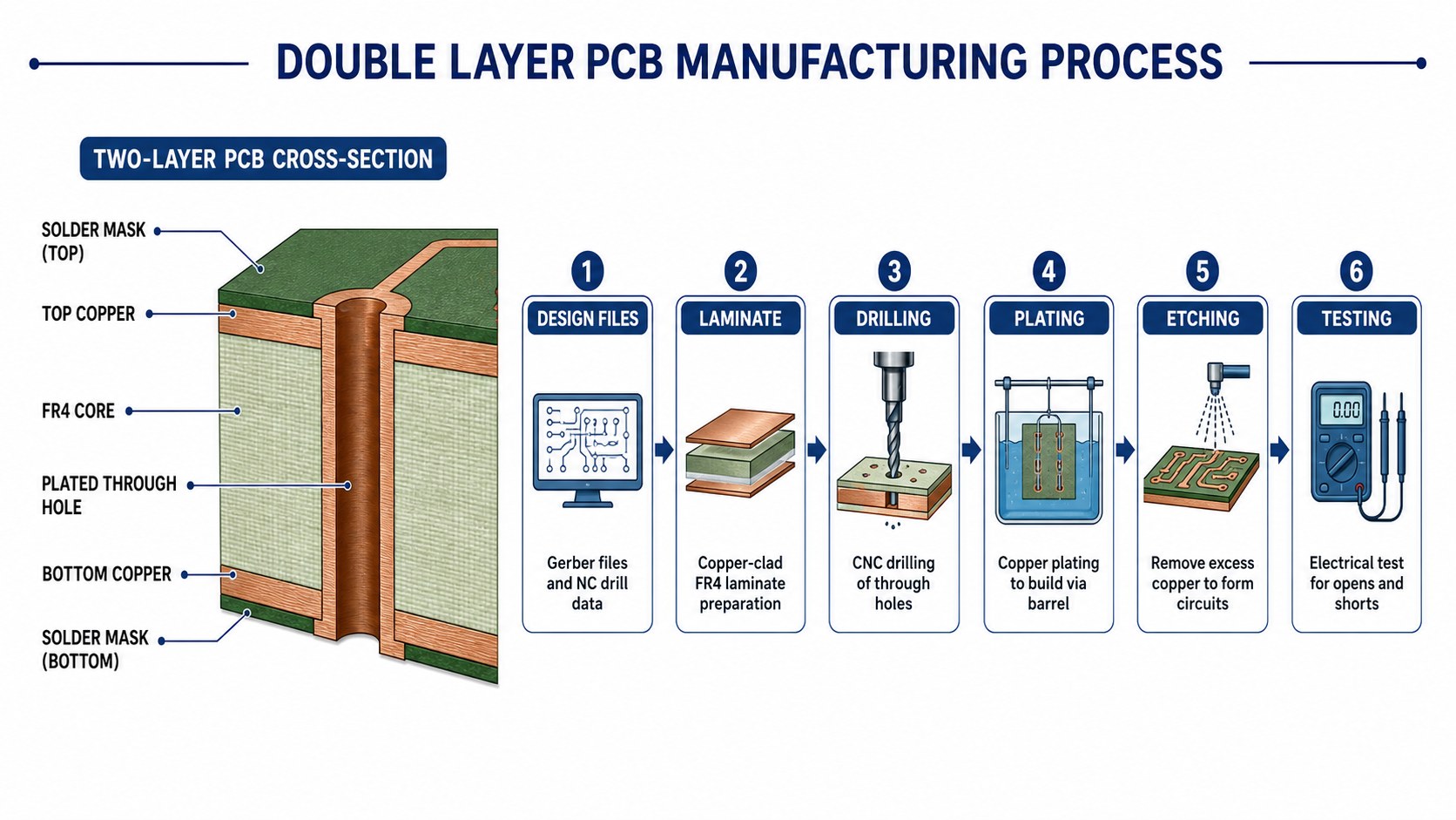
A double layer PCB stackup normally places copper on both sides of an FR4 core, with plated holes joining the two copper layers. This structure gives the designer more options for routing signals, distributing power and creating return paths.
For low-speed control electronics, one side may carry most routing while the other side supports power and ground paths. For power or LED circuits, copper width, heat path and via placement become more important. For assembly-heavy designs, component placement and test access may matter more than the copper layers themselves.
FR4 Materials, Tg Options and Copper Weight
FR4 material and copper weight should be selected before price comparison, because both change how the board is built. EBest Circuit capability records include FR4 low Tg, mid Tg, high Tg and special material options, and list FR4 high-Tg layer capability from 1-10 layers as a general range with special review for higher layer counts.
For copper, the capability records list FR4 inner copper from HOZ-5OZ as general capability and 5-20OZ as special review; FR4 outer copper is listed from 1OZ-5OZ as general capability and 5-20OZ as special review. A two-layer board with heavy copper should therefore be checked for spacing, etching, solder mask bridge and heat requirements before order release.
Board Thickness, Panel Size and Finish Choices
Board thickness and surface finish should be matched to soldering, mechanical fit and expected handling. Capability records list common processed thickness ranges by finish, including OSP, ENIG, immersion silver, immersion tin and ENEPIG from 0.4-3.5 mm, and HASL from 0.6-3.5 mm. Boards outside the common range need project confirmation.
Finish choice should not be made only by habit. OSP can suit cost-sensitive soldering projects. HASL may fit many conventional through-hole or hand-soldered boards. ENIG is often chosen when flat pads, storage or fine assembly behavior matter. The right finish depends on assembly, storage, contact needs and cost.
Line Width, Spacing, Drill and Annular Ring Checks
Two-layer boards often fail manufacturability review at trace spacing, drill size or annular ring, not at the layer count itself. EBest Circuit capability data lists example FR4 line and space capability such as 4/4 mil general and 3/3 mil special for common copper examples, but the final check depends on copper thickness, board finish and design context.
For plated through holes, do not compare only the nominal drill diameter. The finished hole, plating allowance, pad size, annular ring and tolerance all need to work together. If the pad is too small, the board may pass a visual check but still carry long-term reliability risk.
Double Layer PCB Manufacturing Process
The core process includes file review, laminate preparation, drilling, copper plating, imaging, etching, solder mask, surface finish, routing and electrical test. The process is simple to describe, but each step depends on the files and requirements supplied at RFQ stage.
- File review: Gerber, NC drill, drawing, stackup, quantity and finish are checked.
- Laminate preparation: FR4 copper-clad material is selected and prepared.
- Drilling: through holes, mounting holes and slots are drilled according to the NC file.
- Plating: copper is deposited in through holes to connect top and bottom layers.
- Imaging and etching: unwanted copper is removed to form the circuit pattern.
- Solder mask and legend: mask openings and silkscreen are applied and checked.
- Surface finish: pads receive OSP, HASL, ENIG or another specified finish.
- Routing and test: boards are profiled, inspected and electrically tested.
Plated Through Hole Quality and Via Reliability
Plated through hole quality is one of the most important reliability checks in double layer PCB manufacturing. Every signal or power path that moves from top to bottom depends on drilled hole quality, plating coverage and pad design.
Buyers should identify high-current vias, connector holes, thermal vias and mechanically stressed holes in the drawing or notes. These areas may need larger pads, stronger copper, better test coverage or a DFM correction before manufacturing.
Solder Mask, Silkscreen and Surface Finish Decisions
Solder mask and surface finish affect assembly reliability as much as board appearance. The solder mask must leave enough bridge between pads, avoid unwanted exposed copper and match the assembly process. Silkscreen should remain readable without crossing pads or tight components.
EBest Circuit capability data lists solder mask color options and common surface finishes including OSP, HASL, ENIG, immersion silver, immersion tin, ENEPIG and hard gold fingers. The final finish should be chosen by soldering method, storage life, pad flatness and contact needs.
Cost Drivers in Two-Layer PCB Manufacturing
The main cost drivers are material, board size, copper weight, thickness, finish, drill count, tolerance, test coverage, panelization and quantity. A low unit price is not useful if it leaves out electrical testing, special finish, assembly support or engineering review.
| Cost Factor | Typical Impact | Buyer Check |
|---|---|---|
| Board size | Larger panels consume more laminate | Confirm dimensions and panel quantity |
| Copper weight | Higher copper affects etching and spacing | State finished copper clearly |
| Surface finish | ENIG and special finishes usually change cost | Choose finish by assembly need |
| Drilling | More holes and smaller holes add process load | Send NC drill and finished hole notes |
| Testing | Electrical test prevents hidden opens and shorts | Include test requirement in RFQ |
Prototype, Low-Volume and Production Planning
Prototype and production orders should use the same key manufacturing assumptions whenever possible. If the prototype uses one finish, copper weight or stackup and production changes another, the test result may not represent the final board.
For early builds, a practical plan is to lock the stackup, copper and finish early, then use DFM feedback to adjust holes, pads, solder mask and panelization before larger production. For related prototype planning, see our prototype PCB manufacturing guide.
Double Layer PCB Assembly Support
Two-layer PCB manufacturing should be reviewed with assembly in mind when the board will become a PCBA. Component orientation, test points, solder mask openings, via placement and connector fit can all affect assembly yield.
If EBest Circuit handles both bare board and assembly review, the team can check Gerber data together with BOM, CPL, assembly drawing and testing needs. This is especially useful for connectors, through-hole parts, mixed SMT/THT assemblies and boards with high-current paths. For assembly support, see our PCBA service.
Need bare board plus assembly support?
Share Gerber, BOM, CPL, drawings, quantity and test requirements. We can review the two-layer board and PCBA plan together before quoting.
Testing and Inspection Before Shipment
Electrical testing should be part of a serious double layer PCB manufacturing order. It helps detect opens, shorts and connectivity problems before boards move to assembly or final product testing.
Inspection should also cover solder mask registration, surface finish, hole condition, outline quality and key dimensions. If the board carries power, connectors or field-service risk, mark those features in the drawing so the supplier can understand what matters most.
Double Layer PCB vs Single Layer and Multilayer PCB
A double layer PCB sits between single-sided simplicity and multilayer routing density. It gives more routing freedom than one-sided construction while keeping the manufacturing path simpler than four-layer or higher stackups.
| Board Type | Best Fit | Main Limitation |
|---|---|---|
| Single layer PCB | Very simple circuits and low cost boards | Limited routing flexibility |
| Double layer PCB | General electronics, connectors, moderate routing and PCBA | No internal planes for dense routing |
| Multilayer PCB | High density, power planes, impedance and complex routing | Higher stackup and fabrication complexity |
For broader board selection, the FR4 PCB product page and our double-sided PCB boards article provide related background.
Supplier Questions Before Purchase Order
Before placing a purchase order, ask questions that expose engineering fit, not only price. A reliable supplier should be able to discuss manufacturability, testing and assembly impact in plain terms.
If the order is only for bare boards before assembly, it also helps to compare the quote against a dedicated bare PCB manufacturer RFQ checklist so board fabrication, testing and documentation are reviewed before components enter the project.
- Can you review Gerber, NC drill and drawing before production release?
- What copper weight, trace spacing and board thickness need special confirmation?
- Which surface finish best matches my assembly and storage needs?
- Will the quote include electrical testing and inspection requirements?
- Can you support bare PCB fabrication and assembly if the project moves to PCBA?
RFQ File Checklist for Double Layer PCB Manufacturing
A complete RFQ package lets the manufacturer quote the same board you actually need built. Missing drill data, unclear copper weight or vague testing notes can produce a fast quote that later changes.
- Gerber files or ODB++ package
- NC drill file and finished hole notes
- Board drawing with dimensions, tolerance and thickness
- Material, Tg, copper weight and surface finish requirements
- Quantity, panelization preference and target schedule
- Electrical test, inspection or special reliability requirements
- BOM, CPL and assembly drawing if PCBA is required
FAQ About Double Layer PCB Manufacturing
These questions cover the decisions buyers usually need to settle before quoting a two-layer PCB.
What is double layer PCB manufacturing?
Double layer PCB manufacturing makes a board with copper circuits on the top and bottom sides of an insulating core, connected by plated through holes.
Is a double layer PCB the same as a double-sided PCB?
In most buying and manufacturing discussions, yes. Both terms usually refer to a board with copper features on both sides.
What files are needed for a double layer PCB quote?
Send Gerber or ODB++, NC drill, drawing, material, copper, thickness, finish, quantity, test needs and assembly files if PCBA is required.
What affects double layer PCB price most?
Board size, copper weight, thickness, finish, hole count, tolerance, test coverage, panelization and quantity usually drive price.
Can EBest Circuit assemble double layer PCBs?
Yes. EBest Circuit can review double layer PCB fabrication together with BOM, CPL, assembly drawing and testing requirements when PCBA support is needed.
Final Recommendation
Choose double layer PCB manufacturing when the board needs more routing and reliability than a single-sided PCB, but does not need a multilayer stackup. The best result comes from aligning copper, holes, finish, solder mask, test and assembly before fabrication starts.
To quote a double layer PCB project with EBest Circuit, send Gerber or ODB++, NC drill, drawing, board thickness, copper weight, surface finish, quantity, testing notes, target schedule and any BOM/CPL files to sales@bestpcbs.com. Our team will review the build path, check manufacturability and prepare a practical quotation scope.