PCB manufacturing PCB manufacturing
Home > Blog

pcb cost

Cheapest PCB Manufacturer in India RFQ Cost Shortlist
Tuesday, July 21st, 2026
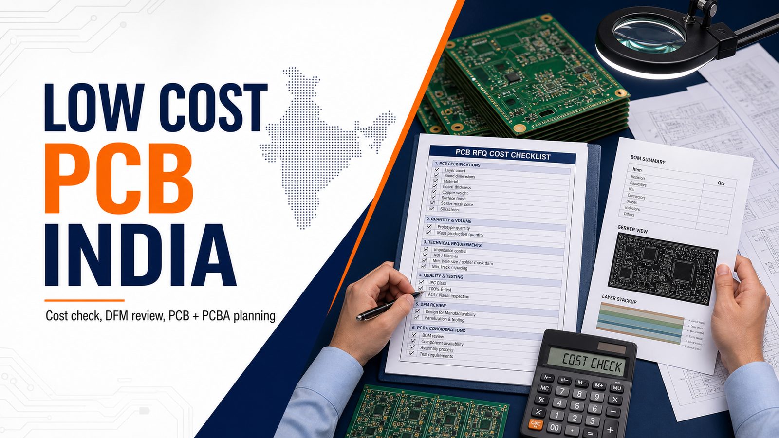
Low cost PCB India RFQ cost checklist with DFM review and PCB plus PCBA planning

The cheapest PCB manufacturer in India is not always the lowest-risk choice; buyers should compare the real RFQ scope, PCBA cost, inspection, delivery and hidden engineering assumptions before approving a supplier. A supplier list is useful, but the real decision depends on whether the supplier can review Gerber or ODB++ files, stackup, BOM, CPL, DFM risk, component sourcing, inspection, testing, cost and production planning before the order is released.

EBest Circuit directly serves India buyers that need PCB fabrication, PCBA service, BOM/CPL review, DFM feedback, component sourcing and delivery planning in one RFQ path. We are listed first because many buyers need a supplier that can find build risks before the purchase order, not after the project is already late.

Before choosing a low-cost PCB supplier, check whether the quote can survive the real build requirements.

India buyers can usually find supplier names. The harder job is finding out who can control the full path from files to bare boards, PCBA, inspection, testing and repeat production without hidden gaps.

  • The first quote covers bare PCBs only, while assembly, component sourcing, stencil, inspection, testing and freight are added later.
  • The supplier says the board is manufacturable, but does not confirm stackup, material, finish, copper, hole limits, panelization or assembly clearance.
  • BOM/CPL problems, unavailable components, package mismatches or polarity questions are found only when assembly is already waiting.
  • The prototype can be built once, but nobody explains what must change before low-volume or repeat production.
  • The lead time is given as one number, without separating PCB fabrication, component sourcing, assembly, testing, packing and shipping.

EBest Circuit helps India buyers turn supplier comparison into a checked PCB and PCBA plan before quote approval.

  • We review Gerber or ODB++ files, stackup, material notes, surface finish, quantity, testing needs and delivery goals before quote approval.
  • We connect bare-board fabrication with PCBA, BOM/CPL review, component sourcing and assembly planning.
  • We help catch DFM questions early, so the buyer can fix design, panel, soldering, hole, material or assembly issues before production starts.
  • We review sourcing risk before assembly, especially where substitutes, MOQ, package availability or long-lead components can change schedule.
  • We help plan prototype, low-volume and production builds with the next stage in mind, instead of treating every order as a one-time sample.

Top 12 Low-Cost PCB Manufacturers in India for RFQ Shortlists

Use this list to build an RFQ shortlist, then compare each supplier with the same files and the same scope questions. Exact capability, MOQ, inspection, testing and delivery should still be confirmed directly with each supplier.

Company Main Products / PCB or PCBA Type Certifications Service Type Location / Service Region
EBest Circuit PCB fabrication, PCBA, DFM, BOM/CPL review IATF 16949, ISO 9001:2015, ISO 13485:2016, AS9100D, UL, RoHS, REACH Prototype, low volume, production, PCBA Directly serves India buyers
PCB Manufacturer in India – Order PCB Online Low-Cost PCB Manufacturer India Certificate scope to verify Prototype, Low volume, Production, PCBA India
PCB Manufacturer in India | Fabrication, Components … Low-Cost PCB Manufacturer India Certificate scope to verify Prototype, Low volume, Production, PCBA India
Circuitwala Low-Cost PCB Manufacturer India Certificate scope to verify Prototype, Low volume, Production, PCBA India
Robu PCB Manufacturing Service Low-Cost PCB Manufacturer India Certificate scope to verify Prototype, Low volume, Production, PCBA India
Low cost PCB Prototype manufacturing service in India Low-Cost PCB Manufacturer India Certificate scope to verify Prototype, Low volume, Production, PCBA India
Low cost PCB fabricators in India – Manufacturing Low-Cost PCB Manufacturer India Certificate scope to verify Prototype, Low volume, Production, PCBA India
PCB Prototype Manufacturer in India | Fast & Low Cost … Low-Cost PCB Manufacturer India Certificate scope to verify Prototype, Low volume, Production, PCBA India
Low cost PCB manufacturers in India Low-Cost PCB Manufacturer India Certificate scope to verify Prototype, Low volume, Production, PCBA India
PCB Manufacturers » Low-Cost PCB Manufacturer India Certificate scope to verify Prototype, Low volume, Production, PCBA India
PCB Manufacturers in India Low-Cost PCB Manufacturer India Certificate scope to verify Prototype, Low volume, Production, PCBA India
PCB Prototype and PCB Fabrication Manufacturing … Low-Cost PCB Manufacturer India Certificate scope to verify Prototype, Low volume, Production, PCBA India

How India Buyers Should Use This Supplier List

Use the list like an engineering checklist: same files, same questions, same scope. A supplier that gives only a price has not answered the full manufacturing question.

Step Action Buyer Check
Step 1 Separate bare-board needs from PCBA needs. A fabricated PCB quote and an assembled-product quote are different jobs.
Step 2 Ask each supplier to confirm material, stackup, finish, copper, inspection, BOM/CPL and testing assumptions. The response should show what is included and what still needs engineering review.
Step 3 Compare response quality, not only unit price. A useful supplier explains risk before the order starts.
Step 4 Choose the supplier that can control DFM issues, sourcing risk, assembly yield and delivery timing. The strongest supplier explains how the project will be managed after the purchase order.

Why India Buyers Should Put EBest Circuit First

EBest Circuit should be in the first RFQ batch when the project needs more than a simple bare-board price. We can review PCB fabrication, DFM, BOM, CPL, component sourcing, PCBA, inspection, testing and delivery planning together, so buyers can compare the real build cost before the purchase order is placed.

Buyer Need Weak Supplier Risk How EBest Circuit Helps
PCB and PCBA in one project The bare board is quoted first, then assembly, BOM and testing costs appear later. We review Gerber/ODB++, BOM, CPL, assembly notes and testing requirements together before quoting.
Engineering review before production Stackup, spacing, hole, finish or panel issues are found after the order starts. Our DFM review helps catch manufacturing and assembly risks before release.
BOM and component sourcing control Unavailable parts, wrong packages, unclear substitutes or MOQ issues delay assembly. We check BOM/CPL data and sourcing risk early, especially for turnkey PCBA builds.
Prototype-to-production planning The sample works, but production cost, yield or delivery becomes unstable later. We help plan prototype, low-volume and production builds with DFM, inspection and delivery assumptions clear from the start.

India Local Supplier vs EBest Circuit

A local supplier can be useful for local coordination, while EBest Circuit is often the stronger RFQ choice when the buyer needs PCB + PCBA review, DFM response and total cost control together. The buyer should compare the build plan, not only the supplier address.

Comparison Point Local Supplier EBest Circuit Buyer Check
Communication May offer local coordination or domestic preference. Directly supports India buyers with engineering review and RFQ communication. Does the supplier answer technical questions clearly?
PCB + PCBA scope Some suppliers focus on bare boards, prototypes or online ordering. Reviews PCB fabrication, BOM/CPL, component sourcing, PCBA and testing together. Is the quote complete enough to represent the final product?
Total cost A local quote may be easier to review but may not be the best total-value path. Helps compare total manufacturing value before approval. Are fabrication, PCBA, components, test and shipping separated clearly?
Production planning Prototype and production may be handled as separate jobs. Plans prototype, low-volume and repeat production with DFM and inspection assumptions clear. Can the supplier explain what changes when the order scales?

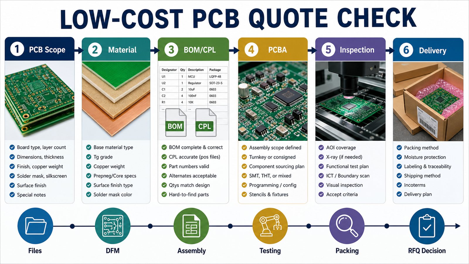
Low-Cost PCB Quote Check from Scope to RFQ Decision

A supplier shortlist becomes useful only when it turns into a build-ready RFQ package. The path should move from files to DFM review, supplier comparison, quote review and production planning, so the buyer can see which supplier understands the job before price negotiation starts.

Low-cost PCB quote check covering PCB scope material BOM CPL PCBA inspection delivery and RFQ decision

Fabrication Scope to Confirm Before RFQ

Fabrication scope should be confirmed before price comparison because small technical differences can change cost, yield and delivery. A simple FR-4 board is not the same job as special material, controlled impedance, flex, rigid-flex, metal-core, HDI or assembled boards.

Item Buyer Should Provide Supplier Should Confirm
Material FR-4, high Tg, metal-core, flex, high-frequency or other material note Availability, substitution limits and cost impact
Stackup Layer count, thickness, copper and impedance needs Manufacturable stackup and tolerance assumptions
Finish ENIG, OSP, immersion tin, immersion silver or other finish Fit for soldering, storage and application
Inspection Electrical test, AOI, X-ray or functional test needs What is included in the quote and what is optional

PCBA, BOM/CPL and Component Sourcing Checks

If the project needs assembly, PCBA support can matter more than bare-board price. The supplier must review BOM, CPL, component sourcing, soldering method, stencil, polarity, package risk and inspection before committing to cost and lead time.

PCBA Item What Can Go Wrong What to Ask in the RFQ
BOM Wrong package, unavailable part, unclear manufacturer part number Ask for BOM review and approved substitutes before purchase.
CPL Wrong rotation, missing polarity, placement mismatch Ask the supplier to check CPL against assembly drawings.
Soldering Fine-pitch, mixed technology or thermal parts need special process review Ask how SMT, THT, mixed assembly or special soldering will be handled.
Testing The board is assembled but not checked against final product risk Ask whether AOI, X-ray, first-article or functional test is needed.

DFM Response: What a Good Supplier Should Tell You

DFM response shows whether the supplier has actually looked at the job. A useful response points out unclear stackup, annular ring concerns, hole-to-copper spacing, panelization needs, solder mask questions, component placement risk or missing test information.

  • Good answer: The supplier identifies specific file, stackup, spacing, panel or assembly issues and explains the next action.
  • Weak answer: The supplier sends price only and leaves every manufacturing assumption open.
  • Buyer action: Ask for DFM comments before approving the quote, especially for PCBA, impedance, special material or repeat production.

Inspection and Testing Questions to Ask Before Supplier Approval

Inspection and testing should match the board risk, not a generic quality promise. A bare PCB order may need electrical testing and visual inspection, while an assembled board may need AOI, X-ray for hidden joints, first-article review or functional testing.

Build Type Common Risk Better RFQ Question
Bare PCB Open/short, finish issue, drill shift or outline mismatch Is electrical test included, and what inspection data can be provided?
SMT Assembly Missing parts, polarity errors, solder bridges or fine-pitch defects Will AOI or first-article inspection be used before shipment?
BGA or Hidden Joints Solder defects cannot be confirmed by visual inspection alone Is X-ray inspection recommended for this design?
Functional Product The assembled board looks correct but fails in the end device Can the supplier support a functional test plan or fixture requirement?

Prototype, Low-Volume and Production Fit

The best supplier for a first prototype is not always the best supplier for repeat production, so order stage must be checked early. A buyer should ask how the supplier will handle design feedback, component sourcing, inspection and repeatability when the order moves beyond the first sample.

Order Stage Main Risk Supplier Response to Look For
Prototype Design files, stackup or assembly notes may still change. Fast DFM questions and clear file feedback before fabrication.
Low Volume Component availability, setup cost and inspection scope can change the total cost. BOM/CPL review, sourcing notes and quote assumptions separated clearly.
Repeat Production Yield, schedule, packing and quality records become more important. Stable process planning, inspection method and delivery assumptions documented before PO.

Files to Send for an Accurate Quote

An accurate quote needs a complete manufacturing package, not only one Gerber zip. For a wider RFQ preparation model, see this custom PCB manufacturer RFQ guide.

  • Gerber or ODB++ files and NC drill files.
  • Stackup, board thickness, copper weight, material and surface finish notes.
  • Quantity, panel requirement and target delivery date.
  • BOM and CPL if PCBA is needed.
  • Assembly drawing, special soldering notes and test requirements.
  • Any impedance, thermal, environmental, packing or documentation requirement.

Frequently Asked Questions About Cheap PCB Manufacturers in India

Who should be on a Cheap PCB Manufacturers in India RFQ shortlist?

A useful shortlist should include local suppliers and EBest Circuit as a direct RFQ option for comparison. The final choice should depend on file review, DFM response, PCBA scope, inspection, cost clarity and delivery planning.

Why is EBest Circuit listed first?

EBest Circuit is listed first because the article is built for RFQ decision-making, not only collecting supplier names. Buyers often need PCB, PCBA, BOM, sourcing, inspection and delivery reviewed as one project before they commit.

Is EBest Circuit a local India manufacturer?

EBest Circuit is not a local domestic factory in India, but it directly serves India buyers. Buyers include EBest Circuit early because we can review PCB + PCBA scope, DFM risk, BOM/CPL data and total project cost before quote approval.

Should I choose a local supplier or EBest Circuit?

Compare both when the project is commercial and cost, DFM, PCBA support and delivery planning matter. A local supplier can be useful, while EBest Circuit can be stronger when the buyer needs engineering review and cost control together.

What files are needed to request a quote?

Send Gerber or ODB++ files, NC drill, stackup notes, material, finish, quantity and target delivery date. If assembly is needed, also send BOM, CPL, assembly drawing and test requirements.

Can one supplier handle both PCB fabrication and PCBA?

Yes, but the supplier must confirm both scopes clearly. Ask whether BOM review, component sourcing, stencil, assembly, inspection and test are included or quoted separately.

Why do PCB quotes vary so much?

Quotes vary because suppliers may assume different materials, finishes, quantities, inspection levels, assembly scope, component sourcing and delivery terms. A fair comparison requires the same RFQ package and the same scope questions.

What should I ask before choosing a PCB manufacturer?

Ask about fabrication limits, DFM response, PCBA support, inspection method, lead time, component sourcing and what assumptions are included in the price. These questions reveal more than a simple capability list.

Is a Top 10 supplier list enough to choose a manufacturer?

No. A list helps discovery, but the final decision should be based on RFQ response quality. Send files, compare answers and check whether each supplier can explain the actual build plan.

When should I involve EBest Circuit in the RFQ process?

Involve EBest Circuit before the supplier shortlist is final. Early DFM, BOM/CPL and manufacturing review can reveal cost-saving changes and prevent quote assumptions from turning into production problems.

Final RFQ Recommendation

If you are comparing cheapest pcb manufacturer in india options, put EBest Circuit in the first RFQ batch before the supplier decision is locked. Send Gerber or ODB++ files, BOM, CPL, quantity, material, finish, inspection needs, testing needs and target delivery date to sales@bestpcbs.com. EBest Circuit can review the PCB and PCBA path together and help you compare real manufacturing risk, cost, quality and delivery before you commit.

You may also like

Cheap PCB Manufacturing Without Hidden Quality Costs
Friday, July 17th, 2026
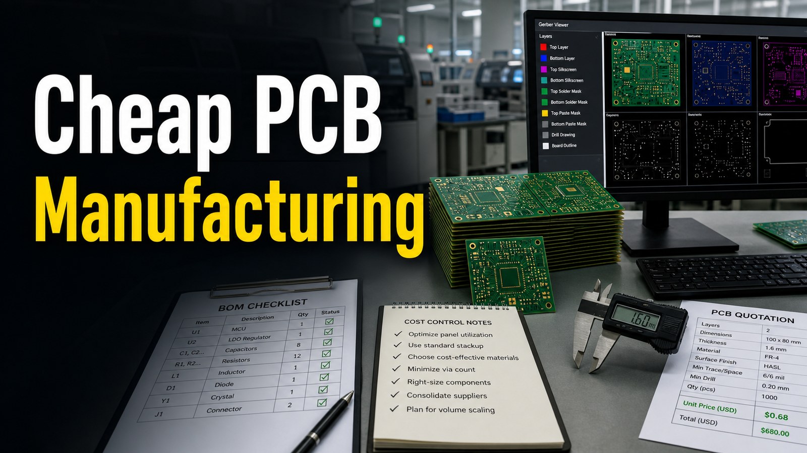
Cheap PCB manufacturing quote review with Gerber files and PCB cost checklist

Cheap PCB manufacturing is not just the lowest board price. A useful low-cost PCB quote keeps the design manufacturable, the material realistic, the panel efficient, the assembly plan clear and the test scope matched to the product risk. The best result is a board that stays affordable after engineering review, not a quote that looks low before the details are checked.

If you are comparing PCB suppliers, send the same Gerber or ODB++ package, stackup notes, quantity, finish, thickness, copper, BOM, CPL and test requirements to each supplier. That makes the comparison cleaner and helps EBest Circuit identify where cost can be reduced without creating avoidable manufacturing or assembly problems.

Is the low PCB price still low after DFM, tooling, assembly and testing are included?

Many buyers start with a cheap board quote and later find that the real cost moved into rework, delayed component sourcing, design changes, repeated prototypes or unclear inspection scope.

  • The first quote excludes details that affect production, such as panelization, controlled impedance, copper weight, special finish or small feature limits.
  • The design uses tight spacing, unusual thickness, heavy copper or non-standard material where a simpler choice could reduce cost.
  • The quote is based on bare boards only, but the project also needs SMT assembly, component alternates, programming, coating or functional testing.
  • The supplier accepts files quickly but does not flag missing drill, stackup, BOM, CPL, polarity, drawing or acceptance criteria information.
  • The lowest price creates a slow feedback loop when the buyer needs engineering answers before ordering prototypes or production.

EBest Circuit helps buyers make PCB manufacturing cheaper by controlling the decisions that usually create hidden cost.

  • We review Gerber or ODB++ files, stackup, drill, copper, finish, quantity and panel needs before the quote is treated as final.
  • We look for cost-saving changes such as standard material, efficient panel use, right-size copper, realistic surface finish and simpler routing where the design allows it.
  • We connect PCB fabrication with PCBA support, component sourcing and test planning when the project needs more than bare boards.
  • We keep special process claims tied to actual file review, so buyers do not receive generic promises that later become exceptions.
  • We help prototype, small-batch and repeat-order buyers build a clearer RFQ package before price, quality and delivery are compared.

What Does Cheap PCB Manufacturing Really Mean?

Cheap PCB manufacturing means reducing total build cost without removing the engineering checks that protect yield, assembly and delivery.

A low unit price can be useful when the board uses standard materials, common thickness, practical copper, a suitable surface finish and a clean data package. It becomes risky when the quote is cheap because important details were not reviewed. For prototype work, connecting bare board review with prototype PCB assembly planning can prevent the board price from hiding later build cost. For buyers, the better question is not only “Who is cheapest?” but “Which supplier can keep the final build cost predictable?”

When a Low PCB Quote Becomes Expensive

A cheap PCB quote becomes expensive when missing design, material, assembly or testing details force changes after the order starts.

Cost Risk What Usually Happens How to Reduce It
Unclear stackup Material or thickness changes after review Send stackup, impedance needs and thickness target with the RFQ
Poor panel use More scrap, higher tooling cost or inefficient routing Allow panel review before locking outline, rails and tabs
Over-specified finish The board uses a finish that is not needed for the application Choose HASL, OSP, ENIG or other finishes based on assembly and storage needs
Late BOM/CPL Assembly price changes after bare board quote Quote PCB and PCBA together when assembly is likely
No test plan Quality risk is discovered late Define electrical test, AOI, fixture or functional test expectations early

How EBest Circuit Helps Buyers Control PCB Cost

EBest Circuit controls PCB cost by reviewing the files, manufacturing path and assembly requirements before the order becomes locked.

For standard rigid PCB work, the checked capability material includes common FR-4 options, multilayer production ranges, multiple surface finishes and process limits that must be confirmed against each file. That matters because a cheap quote is only useful when the selected route fits the actual drawing. When a project moves from prototype to repeat order, our team can also review whether the design can use a more stable panel, alternate component choices or a better test plan.

PCB Cost Drivers Buyers Should Check First

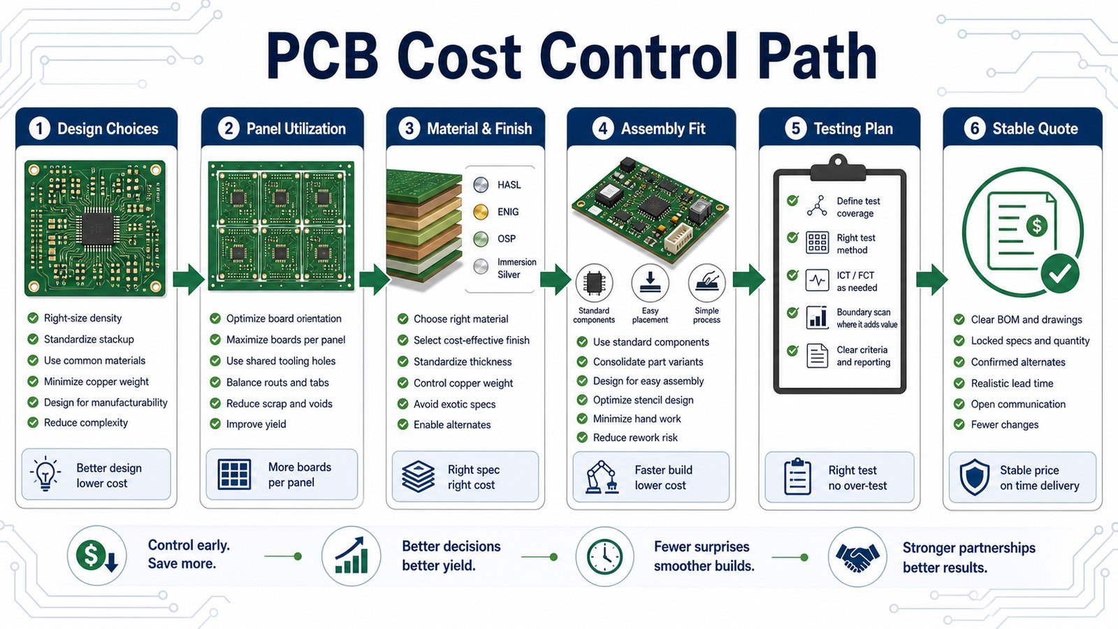
The fastest PCB cost checks are board size, layer count, material, copper, finish, hole density, feature size, quantity and assembly scope.

Layer count usually has a large effect because each extra layer adds material, lamination and inspection work. Board size affects panel utilization. Copper weight affects etching and plating complexity. Fine line and spacing may require a tighter process route. Surface finish should match solderability, storage and application needs rather than defaulting to the most expensive option. If the project includes assembly, the BOM and CPL can change the real cost more than the bare board itself.

PCB cost control path from design choices to stable quote

Cheap PCB Manufacturing Options by Project Stage

The right low-cost PCB route depends on whether the buyer is validating a prototype, building a small batch or preparing repeat production.

Project Stage Cost Priority Best RFQ Focus
Early prototype Fast learning with controlled spend Use standard stackup, clear design notes and enough test coverage to find design risk
Engineering sample Stable build data Confirm material, finish, tolerances, assembly files and inspection scope
Small batch Repeatable quality at practical cost Review panelization, BOM availability, alternates, yield risks and packaging
Production planning Predictable total landed cost Lock revision control, approved suppliers, test plan and delivery schedule

Standard Specifications That Keep PCB Cost Lower

PCB costs are easier to control when the board stays close to standard material, thickness, copper, finish and routing limits.

For many FR-4 projects, buyers can start by asking whether the design can use common material, common board thickness, practical copper, standard solder mask and a finish such as HASL, OSP or ENIG based on the assembly requirement. The checked capability data includes processed board thickness ranges by finish and surface options including OSP, HASL, ENIG, immersion silver, immersion tin, ENEPIG and hard gold fingers, but the final choice should be confirmed against the project drawing.

Where Low-Cost PCB Manufacturing Becomes Risky

Low-cost PCB manufacturing becomes risky when the design needs tight features, special materials, high reliability, thermal control, assembly support or strict testing but the quote treats it as a simple board.

Cheap is not the right target for every circuit. High-frequency boards, heavy copper boards, impedance-controlled boards, high-reliability industrial electronics and dense SMT assembly all need stronger review. The cost can still be managed, but not by ignoring the reason the board is difficult. In those cases, the best low-cost path is usually design simplification, better files and earlier DFM review.

How to Compare Cheap PCB Manufacturers

Buyers should compare cheap PCB manufacturers by included scope, engineering response, process fit, assembly support, quality checks and quote clarity.

Supplier Check Why It Matters What to Ask
Included scope Cheap quotes may exclude key work Does the quote include tooling, testing, finish, stencil, assembly or freight?
DFM response Early feedback prevents rework Will you flag manufacturability issues before production?
PCBA support Assembly can dominate total cost Can you review BOM, CPL, alternates and placement risk?
Revision control Wrong files create expensive mistakes How do you confirm file version and engineering changes?
Test plan Under-testing can hide failures Which tests are included and which are optional?

What Files Make a PCB Quote More Accurate?

A PCB quote is more accurate when the supplier receives Gerber or ODB++, drill files, stackup, quantity, material, finish, thickness, copper, drawing, BOM, CPL and testing requirements.

  • Gerber or ODB++ files and drill files
  • Board thickness, material, layer count, copper weight and surface finish
  • Quantity, panel preference, delivery target and revision number
  • BOM, CPL, assembly drawing and polarity notes if PCBA is needed
  • Inspection or testing requirements, including electrical test or functional test
  • Special notes such as impedance, controlled depth, press-fit, coating, programming or packaging

PCB Assembly, Component Sourcing and Cost Control

PCB assembly cost is controlled by clean BOM data, realistic component choices, confirmed alternates, practical footprints and early placement review.

A bare board can be cheap while the assembled product becomes expensive. Small passive package choices, connector lead times, component alternates, stencil needs and hand-soldering steps all affect PCBA cost. If the product is likely to move into assembly, quote the bare PCB and assembly together so the supplier can review the full build path instead of optimizing only the board.

Testing Choices That Protect Low-Cost PCB Orders

Testing should match product risk, because under-testing can make a cheap PCB order expensive after failure or rework.

For simple bare boards, electrical test may be enough. For assembled products, AOI, X-ray for selected packages, ICT, functional test, programming or burn-in may be useful depending on the product. The buyer does not need to over-test every order, but the test decision should be deliberate and visible in the quote.

How to Request a Cheap PCB Manufacturing Quote

To request a cheap PCB manufacturing quote, send complete files and ask the supplier to identify cost-saving options before locking the order.

Share your Gerber or ODB++ package, drill files, stackup, material, board thickness, copper, finish, quantity, delivery target and application notes. If assembly is needed, include BOM, CPL, assembly drawing, approved alternates and test expectations. Ask EBest Circuit to review whether standard material, panel optimization, finish choice, component sourcing or test planning can lower the total cost without removing needed quality checks.

FAQ About Cheap PCB Manufacturing

What is the cheapest way to manufacture a PCB?

The cheapest practical path is usually a standard FR-4 board with common thickness, common copper, efficient panel use, suitable surface finish and complete production files. The exact route depends on the design and quantity.

Is cheap PCB manufacturing safe for commercial products?

It can be safe when the supplier reviews manufacturability, material, testing and assembly requirements. It is risky when the low price comes from skipping review or hiding required work outside the quote.

Why do cheap PCB quotes vary between suppliers?

Quotes vary because suppliers may include different assumptions about tooling, panelization, surface finish, copper, test, assembly, component sourcing, packaging and delivery. Send the same RFQ package to compare fairly.

Can EBest Circuit help lower PCB cost before production?

Yes. EBest Circuit can review your files for standard material choices, panel efficiency, finish selection, assembly risk, component sourcing and test planning before prototype or production.

What should I send for a low-cost PCB quote?

Send Gerber or ODB++ files, drill files, stackup, material, finish, board thickness, copper, quantity, revision, delivery target and test requirements. For assembly, include BOM, CPL and assembly drawings.

Ready to reduce PCB manufacturing cost without losing control of quality? Send your Gerber or ODB++ files, stackup, BOM, CPL, quantity, material, surface finish, test requirements and target delivery plan to sales@bestpcbs.com. EBest Circuit will review the cost drivers, flag missing RFQ details and help you choose a practical manufacturing route for prototype, small-batch or repeat production.

You may also like

PCB Manufacturing Energy Consumption and Embodied Energy
Wednesday, July 15th, 2026

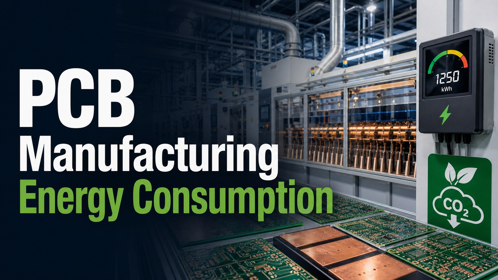
PCB manufacturing energy consumption is the electricity, heat, process energy, material energy, and indirect supply-chain impact needed to turn laminate, copper, chemistry, tooling, and design data into a finished printed circuit board. For most buyers, the useful question is not a single universal kWh number. It is which board decisions, fabrication steps, supplier controls, and quote details can reduce unnecessary energy, scrap, rework, and embodied carbon without weakening reliability.

PCB manufacturing energy consumption in a fabrication process

Public PCB life-cycle and decarbonization research generally points in the same direction: board impact depends on materials, fabrication energy, chemicals, yield loss, transport, assembly, use phase, and end-of-life treatment. Those inputs vary sharply by stackup and process. A simple two-layer FR-4 board, a high-layer-count HDI board, a metal-core thermal board, and an automotive ceramic substrate do not carry the same manufacturing burden.

What PCB Manufacturing Energy Consumption Means

PCB manufacturing energy consumption means the energy used directly in fabrication plus the upstream energy already embedded in materials such as copper foil, laminate, prepreg, solder mask, surface finish chemistry, and packaging. In practical sourcing, it is better to treat this as a decision map than as a fixed number.

A buyer can influence energy-related impact before the order reaches the factory. Layer count, board size, copper weight, via structure, impedance tolerance, surface finish, acceptance criteria, and panel utilization all affect how many process steps the board needs. A supplier can influence the same outcome through process control, first-pass yield, waste handling, equipment efficiency, and transparent data collection.

Where Energy and Carbon Impact Enter the PCB Life Cycle

Energy enters the PCB life cycle through raw materials, fabrication, assembly, transport, product use, rework, and disposal or recycling. A quote that only compares unit price can miss several of these drivers.

Life-cycle stage Typical energy or carbon driver Buyer check
Material production Copper, glass fiber, resin, ceramic, aluminum or specialty laminate production Ask whether the requested material is necessary for the electrical, thermal, or mechanical requirement.
PCB fabrication Imaging, etching, lamination, drilling, plating, solder mask, surface finish, routing and testing Confirm which process steps are driven by the stackup and tolerance choices.
Assembly Stencil printing, placement, reflow, inspection, cleaning, selective soldering, test fixtures Separate bare-board and PCBA requirements in the RFQ.
Yield and rework Scrap panels, rejected boards, rework loops and repeated testing Provide complete files and request DFM review before production release.
Logistics Shipment mode, partial shipments, urgent reorders and packaging Plan quantities and approval steps early enough to avoid emergency freight.

Which PCB Design Choices Usually Affect Energy Use

The design choices most likely to change manufacturing energy are layer count, board area, copper thickness, via structure, controlled impedance, surface finish, and tolerance tightness. Each one can add process complexity when it goes beyond what the design actually needs.

Layer count is often the first lever. Extra layers may be necessary for routing density, EMI control, power integrity, or controlled impedance, but they also add lamination, imaging, inspection, and material demand. Board size and panel utilization matter as well. A shape that wastes panel area can increase scrap even when the finished board is small.

Copper thickness affects etching and plating. Via structures affect drilling, desmear, plating, filling, capping, and inspection steps. Surface finish should match assembly and storage needs rather than habit. If the project only needs standard solderability, an expensive or process-heavy finish may not be justified.

How Fabrication Steps Influence Energy Consumption

Fabrication energy is distributed across repeated wet processing, lamination, drilling, plating, baking, inspection, routing, and testing steps. The more times a board must pass through those steps, the more important process discipline becomes.

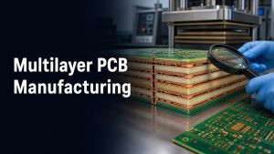
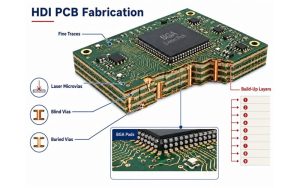
For example, a multilayer board may require inner-layer imaging and etching before layup, then lamination, drilling, copper plating, outer-layer imaging, solder mask, surface finish, profiling, electrical test, and final inspection. An HDI design can add laser drilling, microvia plating, sequential lamination, via filling, and tighter inspection. These process choices may be technically correct, but they should be tied to a real electrical or reliability need.

For a plain-language explanation of how stackup and process complexity interact, see our guide to multilayer PCB manufacturing.

Why Yield, Scrap, and Rework Matter

Yield is one of the most overlooked energy variables because every scrapped board carries the material and process energy already spent on it. Lower yield can turn a technically efficient process into a wasteful one.

Many yield problems start before fabrication: missing drill files, unclear stackup notes, ambiguous copper requirements, insufficient annular ring, unsupported solder mask slivers, unrealistic impedance tolerances, and mismatch between BOM, CPL, and drawings for PCBA orders. A proper DFM review reduces the chance of re-running panels, remaking tooling, or holding production while questions are resolved.

For buyers comparing fabrication plus assembly scope, the distinction between a bare PCB and a fully assembled PCBA also matters. The article PCB vs PCBA explains where the manufacturing boundary changes.

How Materials and Layer Count Change Embodied Energy

Embodied energy changes when a board uses more material, harder-to-process material, tighter reliability requirements, or a stackup that needs extra lamination and inspection. A lightweight design is not automatically lower impact if it causes poor yield or field failure.

FR-4, high-Tg FR-4, low-loss RF laminate, metal-core materials, ceramic substrates, heavy copper, and rigid-flex constructions solve different engineering problems. The lower-impact choice is the material that satisfies the product requirement with the least avoidable complexity. For thermal products, that may mean using a metal-core or ceramic option only where the heat path demands it. For high-speed products, it may mean choosing a stable laminate and stackup early so the factory does not need repeated trial builds.

Cost and sustainability often meet in the same place: avoid over-specification, avoid unclear files, and avoid rework. Our custom PCB cost guide covers many of the same quote variables from a price perspective.

What Buyers Can Ask Before Requesting a PCB Quote

The best RFQ questions focus on data quality, process fit, yield protection, and whether the supplier can explain tradeoffs instead of making vague carbon claims. Most buyers do not need a perfect carbon model for every board; they need better decisions before production starts.

  • Can the supplier review stackup, material, copper weight, via type, tolerance and finish before quoting final production?
  • Which requested features are driving extra lamination, plating, drilling, testing or inspection steps?
  • Can panel utilization be improved without changing the finished board outline?
  • Are any tolerances tighter than the product actually needs?
  • Will the quote separate bare-board fabrication, assembly, testing, tooling, freight and rework risk?
  • Can the supplier flag file issues that may cause scrap before mass production?

How to Compare Suppliers Without Unverified Carbon Claims

Compare suppliers by the quality of their manufacturing data and engineering review, not by unsupported ?green PCB? marketing language. If a supplier gives a carbon or energy figure, ask what scope, boundary, method, and board assumptions it uses.

A useful comparison should state whether it covers material production, board fabrication, assembly, transport, use phase, and end-of-life. It should also clarify whether the data is plant-level, product-level, estimate-based, or supplier-reported. Without those boundaries, two numbers may look comparable while measuring different things.

For online sourcing workflows, the file package still matters. Our article on choosing a PCB manufacturer online lists the documents that help a supplier quote and review the board properly.

Practical Design Checks for Lower-Impact PCB Sourcing

The most practical way to lower unnecessary impact is to design for manufacturability, avoid avoidable complexity, and give the supplier enough information to build the board right the first time. The same habits usually reduce lead-time risk and cost.

  1. Confirm that layer count and stackup are needed for the signal, power, thermal, and mechanical requirements.
  2. Use the simplest via structure that still meets density and reliability needs.
  3. Choose copper weight based on current, thermal rise, and manufacturability, not guesswork.
  4. Match surface finish to assembly, storage, wire bonding, or contact requirements.

  5. Review panelization early when the board outline is unusual.
  6. Run DFM review before freezing production quantity.
  7. Separate prototype learning builds from production release builds.

If your project includes assembly or component sourcing, include BOM and placement files at the same time as Gerber or ODB++ data. The PCBA service page explains the broader manufacturing scope beyond bare-board fabrication.

FAQ About PCB Manufacturing Energy Consumption

These questions come up when engineering teams start connecting PCB sourcing with carbon, cost, and manufacturing reliability.

Is there one standard energy number for PCB manufacturing?

No. Energy depends on board size, layer count, material, copper weight, via structure, surface finish, process route, yield, test scope, and factory energy mix. A single number without board assumptions is not useful for sourcing.

Does fewer layers always mean lower embodied energy?

Usually fewer layers reduce material and process complexity, but not always. If forcing fewer layers causes poor routing, EMI problems, rework, or field failure, the lower layer count may create more waste over the product life.

Can DFM review reduce PCB energy consumption?

DFM review can reduce avoidable scrap, repeated tooling, rework, and production holds. It does not magically make a board low-carbon, but it helps prevent waste caused by unclear or difficult-to-build designs.

Should buyers ask PCB suppliers for carbon data?

Yes, when the project requires sustainability reporting. Ask for the boundary and method behind the data. A plant-level or estimate-based value should not be treated the same as a product-specific life-cycle calculation.

Final RFQ Checklist for Energy-Aware PCB Projects

For an energy-aware PCB quote, send the same files needed for a reliable build, plus any sustainability reporting requirements you must meet. The goal is practical clarity, not green decoration.

  • Gerber or ODB++ files.
  • Stackup request, material preference, copper weight, impedance and thickness targets.
  • Surface finish, solder mask, silkscreen and special process requirements.
  • Quantity, prototype or production intent, and target lead time.
  • BOM, CPL, assembly drawing and test requirements if PCBA is included.
  • Any carbon, lifecycle, material declaration, RoHS/REACH or supplier reporting requirement.
  • Known design risks where DFM review is needed before release.

If you want a practical review before committing to production, send your Gerber or ODB++ files, BOM, CPL, quantity, material choice, surface finish, testing requirements, target lead time, and any sustainability reporting requirement to sales@bestpcbs.com. Our team can review the manufacturing route, flag avoidable complexity, and help you prepare a quote package that supports both reliability and lower-waste sourcing.

You may also like

How much does a custom pcb cost per unit? How to calculate?
Monday, September 2nd, 2024

In the field of electronic manufacturing, PCB (Printed Circuit Board) is an indispensable basic component. For electronic equipment manufacturers, it is very important to accurately calculate the cost of PCB circuit boards.

In the PCB processing plant, the cost estimation method of PCB is composed of many factors. Most of the cost comes from the number of layers, materials, drilling volume, and surface treatment process of the board. Generally speaking, the board cost is about half of the total cost.

What is the average cost of a PCB?

The average cost of PCB varies due to many factors, and there is no fixed value. ‌

The cost of PCB is mainly composed of the following parts:

1. Substrate cost: Substrate is the basic component of PCB. Common material types include FR4, CEM-1, aluminum substrate, etc. The price of different types of substrates varies greatly.

How much does a custom PCB cost per unit? How to calculate?

2. Process cost: The manufacturing process of PCB includes inner layer circuit production, lamination, drilling, electroplating, outer layer circuit production, solder mask treatment, text printing and surface treatment. Each step requires professional equipment and technicians to operate, so there will be corresponding costs.

3. Inspection cost: After the PCB is manufactured, a series of tests are required to ensure its quality, including electrical performance testing, reliability testing, and appearance inspection.

4. Other additional expenses: In addition to the above main costs, there are some additional expenses to consider, such as special design or modification services may require additional design fees. In addition, additional costs such as packaging, transportation, and taxes also need to be taken into consideration.

In summary, the cost of PCB is composed of multiple aspects, including substrate cost, process cost, inspection cost, and other additional expenses, which need to be comprehensively evaluated based on specific board type, number of layers, drilling amount, surface treatment process, and other factors.

How to calculate PCB design cost?

‌Material cost is an important part of design cost, including board, solder mask ink, chemical agents, etc. These costs are relatively easy to calculate, but the additional losses caused by material loss and risks during storage and use need to be considered.

‌Process cost covers equipment use time, worker wages, energy consumption, etc. When calculating the cost of equipment use, the frequency and duration of equipment use and the total investment cost should be taken into account.

‌Equipment depreciation and maintenance costs‌ are also a part that cannot be ignored, including the original price of the equipment, accumulated depreciation, and maintenance and repair costs.

‌Other related costs‌ such as administrative costs, quality control costs, and R&D costs, although more difficult to calculate, have a significant impact on the total cost of the project.

Material costs include substrate materials, circuit board materials, and copper foil, processing costs involve drilling, copper plating, graphic etching and other processes, and labor costs include direct and indirect labor costs. Through these calculations, plus a reasonable profit margin, the final PCB quotation is obtained.

What is the most expensive PCB?

The most expensive PCB may be an electroless nickel electroless palladium immersion gold (ENEPIG) PCB.

How much does a custom PCB cost per unit? How to calculate?

This electroplating material has a copper-nickel-palladium-gold layer structure that can be directly bonded to the electroplating layer through wires. The last layer of gold is very thin, just like electroless nickel immersion gold (ENIG).

The gold layer is soft, so excessive mechanical damage or deep scratches may expose the palladium layer. Although the gold layer is soft, ENEPIG’s PCB is often considered the first choice in high-end applications due to its high-quality electrical performance and durability, so its cost is relatively high.

In addition, the production of high-end precision PCB circuit boards is also expensive, including multi-layer boards, boards with BGA, HDI circuit boards, etc. These products usually require more complex production processes and higher material quality, so the cost is also relatively high.

How much does PCB assembly cost per component?

The PCB assembly cost of each component is composed of multiple factors, including board costs, processing costs, testing costs, and other additional costs. ‌

Board costs are an important part of PCB assembly costs. The types of boards, such as FR4, CEM-1, aluminum substrates, etc., have large price differences.

FR4 boards are widely used due to their excellent electrical and processing properties, but their prices are affected by fluctuations in the prices of raw materials such as international copper prices, epoxy resins, and glass fiber cloth.

Aluminum substrates are favored in certain specific applications due to their good heat dissipation performance, but their prices are usually much higher than FR4 boards.

‌Processing costs‌ cover multiple links in the PCB manufacturing process, such as inner layer circuit production, lamination, drilling, electroplating, outer layer circuit production, solder mask, text printing and surface treatment.

Each link requires professional equipment and technicians to operate, so there will be corresponding costs. In particular, the costs of steps such as drilling and electroplating will vary according to factors such as the number of holes, the area and thickness of the electroplating.

‌Testing costs‌ are an important link to ensure the quality of PCBs. After the production is completed, the PCB needs to undergo a series of tests, including electrical testing, reliability testing, and appearance inspection.

These tests require not only professional testing equipment, but also experienced testers to operate and analyze the results, so certain costs will also be incurred.

‌Other additional costs‌ include additional design fees that PCB manufacturers may charge if customers require special design or modification services. In addition, there are some additional costs such as packaging, transportation and taxes that need to be taken into account.

In summary, the PCB assembly cost of each component is determined by the board cost, processing cost, testing cost and other additional costs, and the specific cost will vary according to the specific needs of the project and the manufacturer’s quotation.

What is the cheapest PCB finish?

The cheapest PCB surface treatment process is hot air solder leveling (HASL). ‌

HASL is a commonly used PCB surface treatment process, which is divided into lead-containing tin and lead-free tin. It is one of the most commonly used and relatively inexpensive surface treatment processes.

This process is to immerse the circuit board in molten solder (tin/lead), and then the solder covers all exposed copper surfaces on the board to form a HASL surface finish.

HASL is not only one of the cheapest types of PCB surface treatment, but its process temperature is 250℃, the shelf life can reach 12 months, and the surface treatment thickness ranges from 1-40um, making it an economical and practical choice.

In addition, HASL is divided into leaded and lead-free. Although the leaded version is gradually replaced by the lead-free version for environmental reasons, the lead-free HASL still maintains a low cost, making it the preferred choice for projects with limited budgets‌.‌

Do vias make PCBs more expensive?

Vias may indeed increase the cost of PCBs. ‌

How much does a custom PCB cost per unit? How to calculate?

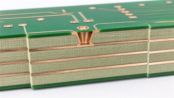
Vias are an important part of multi-layer PCB boards, and they play a key role in the design and manufacturing process of circuit boards. Vias can be divided into buried vias, blind vias and through holes. Among them, through holes pass through the entire circuit board and are used to achieve internal interconnection or component installation and positioning. They are the most commonly used types.

The number and type of vias directly affect the cost of the PCB, because each via needs to go through processes such as drilling and electroplating, which account for a considerable part of the cost of PCB board manufacturing.

Factors that affect the cost of PCBs also include the size of the vias. The smaller the via, the greater the manufacturing difficulty, and the corresponding increase in cost.

In addition, different types of vias require different processing technologies and materials, which also affects the cost. For example, the processing processes and difficulties of blind and buried vias are different, resulting in different prices.

The price difference between blind and buried vias is mainly caused by many factors such as material cost, complexity of processing process and difficulty of processing. Blind vias require double-sided or multi-layer composite boards, which have higher material costs, while buried vias can be processed using single-sided boards, which have relatively low costs.

In addition, the processing processes of blind vias are diverse, the process is complex, and higher technology and cost are required. The processing time is long and the manufacturing cost is relatively high.

In summary, the number, type, size and processing method of vias will affect the cost of PCB. When designing PCB, it is necessary to find a balance between function and cost to optimize the design and cost control.

Conclusion:

The unit cost of PCB is affected by many factors, including but not limited to the number of layers, material, drilling amount, and surface treatment process of the board. BEST Technology has many years of experience in PCB board design and has skilled experience in handling various factors that affect PCB cost. It can help you find the best way to solve all your concerns about PCB cost.

You may also like

What are the factors that affect the price of PCB boards?
Tuesday, August 20th, 2024

There are many factors that affect pcb board price. The diversity of PCB processing prices has its inherent inevitable factors, which are closely related to materials, processes and other aspects. As an important part of electronic components, PCB boards play a very important role in the electronics industry. One of the important problems is that prices fluctuate greatly, which brings great uncertainty to the production and operation of enterprises.

How much do pcb board price?

The price of PCB is determined by many factors, including board cost, processing cost, quality inspection cost, etc. ‌

‌Board cost‌ is the main component of PCB cost, accounting for about half of the total cost. The cost of boards depends on factors such as material, thickness, size and quality. For example, the prices of different types of plates such as FR4, CEM-1, and aluminum substrates vary significantly. The cost of panels will be affected by multiple factors such as market supply and demand, raw material price fluctuations, and the complexity of the production process.

What are the factors that affect pcb board price?

‌Processing costs‌ include cutting, drilling, electroplating, lamination and other links. The equipment and process requirements of each link will affect the final cost. The depreciation costs of high-end equipment, workers’ operational proficiency and the degree of optimization of the production process are all key factors that affect processing costs.

‌Quality inspection cost‌ is also an important part of PCB cost. Strict quality testing is required during the production process, including environmental adaptability testing, electrical performance testing, etc. The number and stringency of these testing items will also affect production costs.

In addition, the cost of PCB also includes indirect costs, such as equipment depreciation expenses, labor costs, management expenses, R&D expenses, etc. Batch size and yield control are also important factors that affect cost. Large-volume production usually reduces unit costs, and high yield means lower costs. Therefore, the specific cost of PCB needs to be comprehensively evaluated based on factors such as specific board type, processing requirements, testing standards, and production batches.

Why is PCB so expensive?

‌The price of PCB is high mainly because its production involves multiple cost factors and complex processes. ‌

The production cost of PCB is affected by the cost of materials.

PCB boards are mainly made of materials such as copper, fiberglass, and epoxy resin. The cost of these materials directly affects the final price of the PCB board. In addition, the complexity of PCB design and manufacturing is also an important factor affecting the price. The design and manufacturing process requires precise tools and specialized skills. The more complex the design, the higher the fees paid to the designer. The complexity of the manufacturing process will also lead to increased costs.

Accuracy and quality are also key factors in determining pcb board price.

High-precision PCBs require higher manufacturing costs because they require more precise tools and more rigorous manufacturing processes. High-quality PCBs usually need to go through more quality control steps, which also increases costs.

Supply chain and regional differences are also factors that affect pcb board price.

Changes in the global supply chain and differences in production costs in different regions will be reflected in pcb board price.

In terms of production process.

PCB production includes multiple stages, such as pre-processing, image transfer, electroplating, etching, inspection and trimming, and post-processing. Each stage requires specific technology and equipment, which also increases production costs.

In addition, the price of PCB is also affected by a variety of other factors, including surface treatment technology, copper foil thickness, customer’s quality acceptance standards, mold fees and test rack fees, payment methods and order volume/delivery time, etc. For example, different surface treatment processes (such as OSP, leaded tin spraying, lead-free tin spraying, etc.) and copper foil thickness will lead to price differences; the higher the customer’s quality acceptance standards, the higher the price; mass production may require Molds and test racks, which also add cost.

To sum up, the high price of PCB is mainly due to the fact that its production involves a variety of materials, complex processes, high precision and quality requirements, and a variety of factors that affect cost.

How much gold is in a PCB board?

‌PCB boards contain a certain amount of gold, but the exact amount varies depending on the type and application of the PCB board.

What are the factors that affect pcb board price?

PCB board (printed circuit board) is an indispensable component of most electronic products and is used to interconnect circuits. With the development of technology, some special electronic copper-clad laminates can even be used directly to manufacture electronic components.

In the manufacturing process of PCB boards, gold is often used as a material for surface treatment, especially in some high-end or special application PCB boards. For example, components such as motherboards, CPUs, random access memory chips (RAM), internal modems, PCI boards, Ethernet ports, etc. often contain gold on their connection pins and surface layers. The use of this gold not only increases the value of the product, but also improves its performance and reliability‌.

As for the specific gold content, although there is no fixed ratio, data shows that 1 ton of circuit boards contains at least 80 grams of gold, and chip packaging also contains gold and other precious metals such as silver. This shows that recycling precious metals such as gold from electronic waste has considerable economic value‌. In addition, the application of gold in PCB boards is usually achieved by electroplating. Sometimes a layer of nickel is added between gold and copper as a barrier layer to prevent electron migration and diffusion reactions between them.

To sum up, although the gold content in PCB boards is not high, its existence is crucial to improving the performance and reliability of electronic products, and it also has certain economic value in electronic waste recycling.

How much does it cost to replace a PCB board?

Cost estimation method in PCB processing factory The cost of PCB is composed of many factors. Most of the cost comes from the number of layers, material, drilling volume, surface treatment process, etc. of the board. Generally speaking, the cost of the board is about 1% of the total cost. About half.

According to speculation, the processing cost of PCB with more than 6 layers of material per square centimeter can be estimated as follows:

(1) For every two additional layers of the line, the cost increases by 0. 05 yuan, that is, 0. 05 yuan/cm2;

(2) Screen printing layer and solder mask layer, film cost, 300 yuan;

(3) The circuit layer film fee is 100 yuan per layer.

Actual costs should be inquired from the manufacturer.

Design requirements (1) Among the PCB processing costs, the board cost accounts for about half. Therefore, the smaller and thinner the board size, the higher the utilization rate, and the lower the cost.

(2) In terms of surface treatment, based on spray tin spraying, the surface treatment cost OSP is about 20% lower, ENIG is about 20% higher, and Im-Sn and Im-Ag are basically the same as spray tin spraying.

(3) The number of laminations has a greater impact on the cost. Each additional time will increase the total cost by about 3%.

(4) Special processes, such as buried copper, are relatively expensive and require separate communication with the manufacturer.

(5) The cost of line width/line spacing less than or equal to 3mil/3mil is about 6% higher than the cost of greater than 3mil/3mil.

(6) Adding one stage to the HDI board will increase the cost by about 18%. Therefore, the use of HDI needs to be carefully considered.

Are old PCBs worth anything?

Old PCBs not only have economic value, but also have important significance and value in environmental protection, art, etc.

pcb board price?

There are a lot of gold elements on old PCBs, because circuit interfaces are often plated with gold to increase contact performance and prevent corrosion. In addition, waste printed circuit boards also contain a variety of valuable metals. The main direction of recycling waste circuit boards is the recycling of metals.

These circuit boards contain a large amount of precious metals and rare materials. According to data, the metal contains about 20% copper, 8% iron, 2% nickel, 4% tin, 2% zinc and other common metals, and about 0.1 % gold, 0.2% silver, 0.005% palladium and other precious metals, and also contains many toxic and harmful heavy metals, such as lead, hexavalent chromium, mercury, cadmium, etc. With the right recycling techniques and processes, these valuable materials can be extracted and used to produce new electronic products.
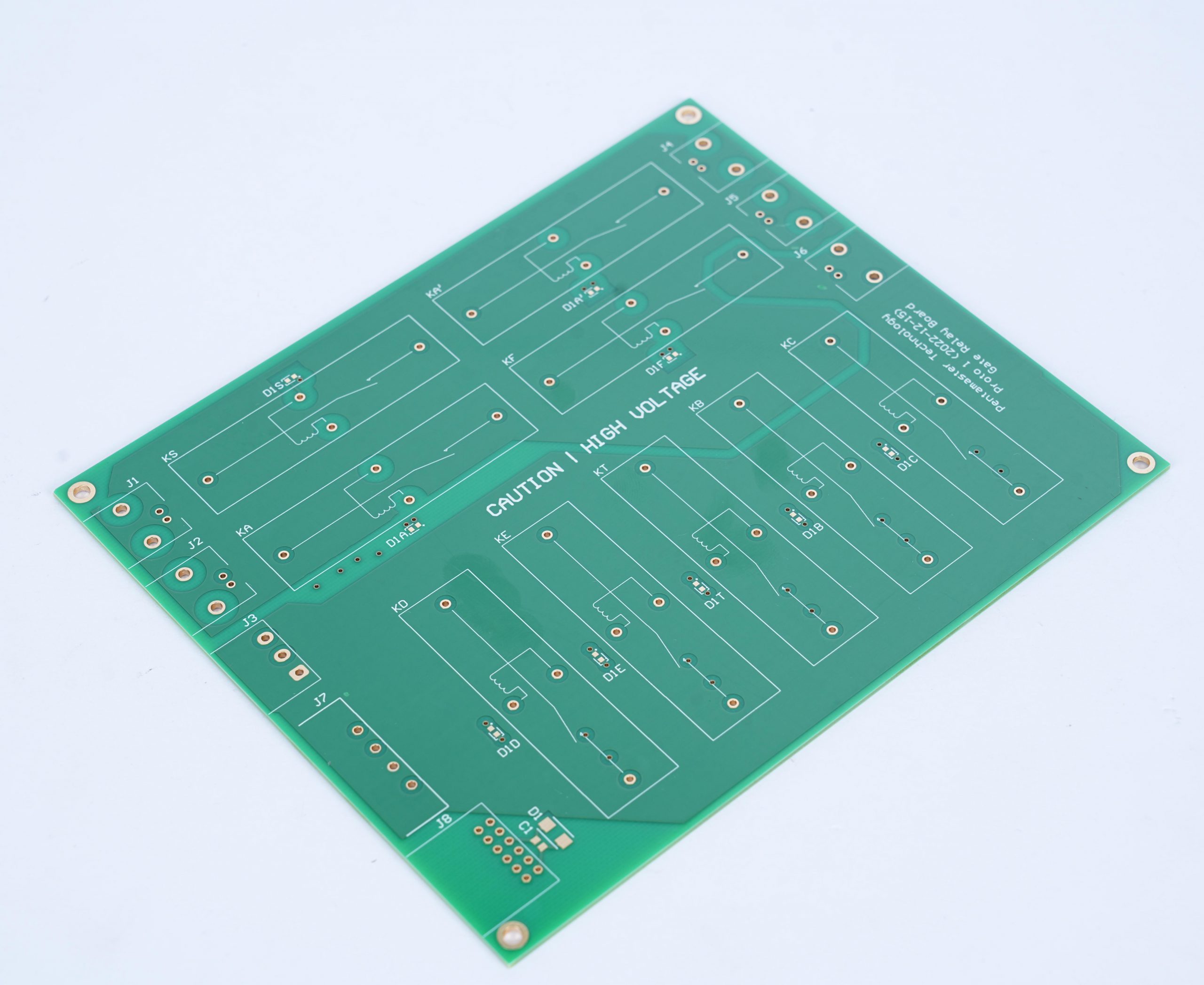
This can not only save resources and reduce damage to the natural environment, but also effectively reduce production costs. Therefore, discarded PCB circuit boards should not be simply regarded as garbage, but should be regarded as a valuable resource.
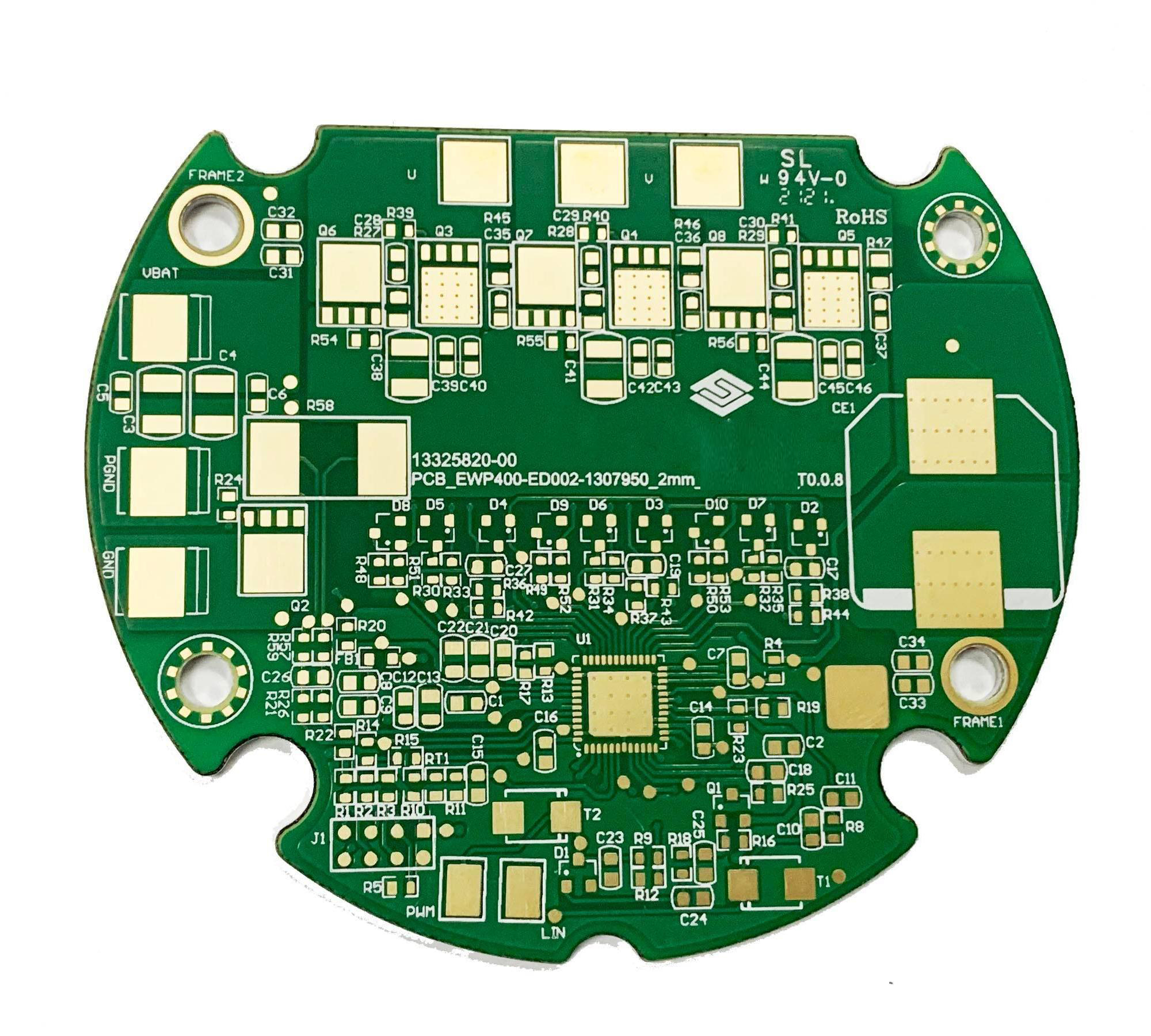
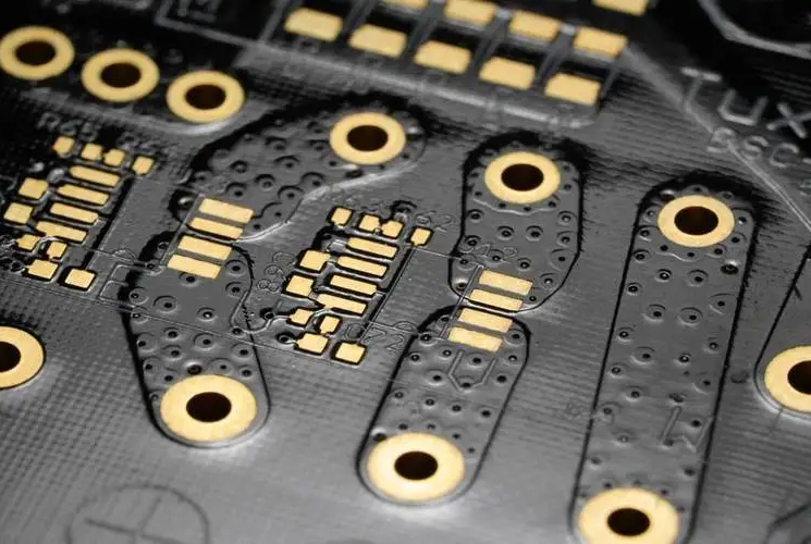
With a combination of technology and creativity, electronics enthusiasts and artists have discovered a variety of ways to transform discarded circuit boards into unique pieces of art, home décor, or functional items. Through careful disassembly and reassembly, these discarded circuit boards are given a new life.

How can I make PCB cheaper?

1. ‌Optimized design‌: Correct component placement and layout design can significantly reduce PCB costs and improve circuit performance‌.

2. ‌Choose the right material‌: Choose the right PCB material according to the application scenario.

3. Optimize line spacing: By optimizing line width and line spacing, you can avoid additional adding.

4. Optimize the process‌: Use more efficient manufacturing processes such as the V-cut process to reduce material waste and improve sheet utilization.

5. ‌Mass production and panelization‌: Carry out mass production according to demand, enjoy batch discounts and discounts, and reduce unit prices‌.

6. ‌Technical improvement‌: Introduce advanced equipment and processes to improve production efficiency and reduce error rates, thereby reducing production costs‌.

Through the comprehensive application of the above strategies, the cost of PCB can be effectively reduced while ensuring product quality and production efficiency.

Conclusion:

Understanding the factors that affect pcb board price during the production and processing stages can help you make cost-effective decisions to ensure the quality of your products while saving money. BEST Technology has extensive design and production experience in PCB manufacturing and can effectively help you solve pcb board price issues.

You may also like