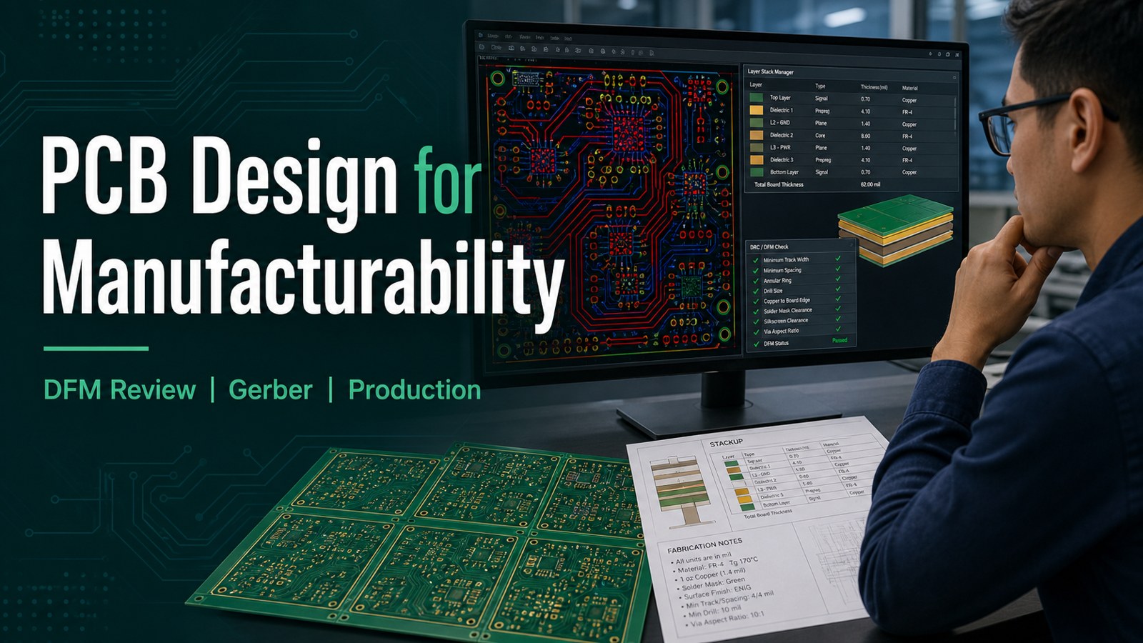
PCB design for manufacturability means checking whether a board can be fabricated, assembled, inspected and repeated before production files are released. A useful DFM review does not only look for design-rule errors. It checks whether the stackup, trace spacing, drill sizes, annular rings, copper balance, solder mask, component clearance, panelization and test access all fit the intended PCB manufacturing and PCBA process.
For buyers, DFM is a cost and schedule control step. It helps prevent a design from moving into prototype or production with hidden fabrication risk, missing files, assembly clearance problems or quote assumptions that later change the delivery plan.
Before releasing PCB files, make sure the design is ready for the way it will actually be built.
Engineering and purchasing teams often run into avoidable delays when a design is quoted before the manufacturing package is complete.
- The Gerber set looks complete, but drill files, stackup notes, controlled impedance or fabrication drawings are missing.
- Trace width, spacing, via drill, annular ring or copper-to-edge clearance fit the CAD rules but not the selected supplier’s process window.
- Assembly files arrive after the bare-board quote, so BOM/CPL errors and component clearance issues are found late.
- Panelization, fiducials, tooling rails or test access are not considered until the build is already scheduled.
- A prototype passes once, but the same files are not stable enough for low volume or repeat production.
EBest Circuit reviews PCB design files with fabrication, assembly and quotation readiness in one workflow.
- We review Gerber, ODB++, NC drill, stackup, fabrication drawings, material notes, surface finish and quantity before quote confirmation.
- For assembled boards, we check BOM, CPL, polarity notes, assembly drawings, placement risk and test expectations with the PCB manufacturing scope.
- We help buyers identify manufacturability issues early so the quotation reflects the real build, not a simplified version of the project.
- We support prototype, low-volume and repeat production planning when the same design must move beyond first samples.
PCB Design for Manufacturability in One Practical Answer
PCB design for manufacturability is the review process that turns a PCB layout into a buildable production package. It checks whether the board geometry, stackup, material, drill map, copper features, solder mask, silkscreen, panelization and assembly data can move through manufacturing without avoidable holds.
Why DFM Matters Before PCB Manufacturing
DFM matters because most PCB delays are cheaper to fix before files enter production. A small clearance adjustment, stackup clarification or BOM correction can prevent re-quotes, production holds, late component surprises and repeat sample builds.
If your design is moving from layout to build planning, the PCB design and manufacturing DFM workflow is a useful companion for organizing files before supplier review.
File Package Buyers Should Prepare
A DFM-ready RFQ package should include the files needed to quote, fabricate, assemble and inspect the board. For bare boards, send Gerber or ODB++, NC drill, stackup, fabrication drawing, material, copper weight, surface finish, board thickness, quantity and acceptance notes.
For PCBA, also send the BOM, CPL, assembly drawing, polarity notes, test instructions, programming needs and any packaging or labeling requirements. For fabrication scope review, see EBest Circuit’s PCB manufacturing capabilities.
Trace, Space, Hole and Annular Ring Checks
The first technical DFM check is whether copper features fit the intended process window. Review minimum trace width, trace spacing, via drill, annular ring, hole-to-copper clearance, copper-to-board-edge clearance, solder mask dams and copper balance.
| DFM Area | What to Check | Why It Matters |
|---|---|---|
| Trace and spacing | Minimum copper width, gap and high-density areas | Prevents etching, shorting and yield risk |
| Drill and via | Drill size, aspect ratio, annular ring and tolerance | Controls plating reliability and registration risk |
| Board edge | Copper, slots, castellations and routing clearance | Prevents exposed copper and mechanical damage |
| Solder mask | Mask bridge, expansion and exposed pads | Supports solderability and assembly yield |
Stackup, Copper and Material Checks
Stackup review confirms whether layer count, dielectric thickness, copper weight and material selection match the electrical and manufacturing goal. Controlled impedance, high-speed routing, thermal behavior and high-current areas all depend on stackup clarity before the quote is approved.
Need a DFM check before PCB production?
Send Gerber or ODB++, drill files, stackup, quantity and assembly files. EBest Circuit can review manufacturability, quote readiness and PCBA risk before you approve the build.
Gerber/ODB++ | Drill | Stackup | BOM/CPL | Quantity | Testing
Solder Mask, Silkscreen and Board Outline Checks
Mask, marking and outline details should be checked because they affect assembly, inspection and mechanical fit. Review solder mask expansion, mask slivers, exposed copper, component polarity marks, silkscreen over pads, board slots, cutouts, V-cut lines and routed edges.
Assembly Clearance and PCBA DFM Checks
PCBA DFM checks make sure the board can be assembled, inspected and tested after fabrication. Review component spacing, connector overhang, tall components, fiducials, tooling rails, stencil needs, polarity, thermal relief, keep-out areas and access for AOI, X-ray or functional test.
For turnkey builds, EBest Circuit’s PCBA and SMT assembly support can align BOM/CPL review with PCB manufacturing instead of treating assembly as a separate late-stage problem.
Testing, Panelization and Production Release
DFM is not complete until the supplier knows how the board will be panelized, inspected and released. Check electrical test, impedance test when required, AOI, X-ray for hidden solder joints, functional test access, fiducials, tooling holes, rails, breakaway tabs and packaging needs.
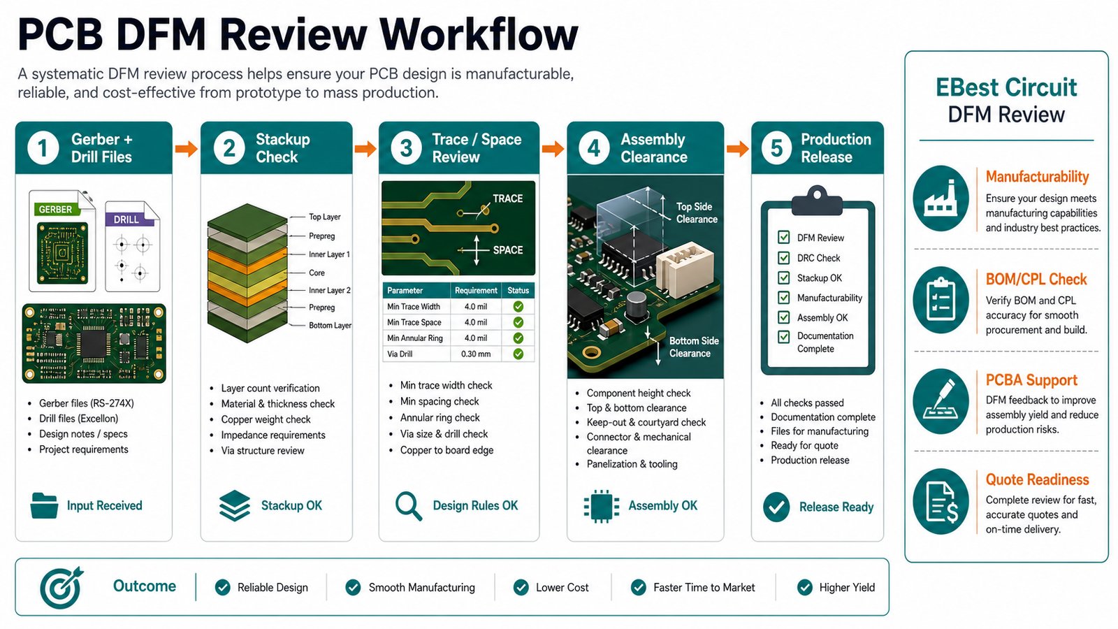
EBest Circuit DFM Review Workflow
EBest Circuit uses DFM review to connect engineering files with manufacturing cost, lead time and quality planning. The review starts with file completeness, then moves through stackup, copper features, material, finish, assembly data, inspection needs and quotation scope.
For early builds, the prototype PCB manufacturing RFQ guide explains how to package files before first samples. For small batch planning, use the low volume PCB manufacturing guide to plan repeatability after the prototype stage.
DFM Checklist Before You Request a Quote
Use a DFM checklist before RFQ so the first supplier response is based on complete, buildable information.
- Gerber or ODB++ files match the intended revision.
- NC drill, stackup and fabrication drawing are included.
- Material, board thickness, copper weight and surface finish are clear.
- Minimum trace, spacing, via, slot and annular ring values are known.
- Controlled impedance, high-current or thermal requirements are marked.
- BOM, CPL and assembly notes are ready if PCBA is included.
- Testing, packaging, labeling and target delivery needs are defined.
Common PCB DFM Mistakes
The most common DFM mistake is assuming that passing CAD rules means the board is ready for production. CAD rules may not reflect the selected supplier, material, assembly process, inspection method or quantity plan.
| Mistake | Production Risk | Better Action |
|---|---|---|
| Missing stackup notes | Wrong thickness, impedance or material assumption | Confirm stackup before quote approval |
| Late BOM/CPL files | Assembly risk found after board quote | Send PCBA files with the RFQ |
| No panelization plan | Assembly handling and cost changes later | Ask supplier to review rails and fiducials |
| Only comparing price | Cheap quote may exclude review, testing or repeatability | Compare DFM scope and build support |
Use EBest Circuit as your PCB DFM quote checkpoint.
A practical DFM review can reveal file gaps, stackup risk, assembly questions and cost drivers before production starts.
DFM | PCB fabrication | PCBA | Testing | Repeat production
PCB Design for Manufacturability FAQ
What does PCB design for manufacturability mean?
It means reviewing a PCB layout and file package against real fabrication, assembly, testing and production requirements before the board is released for manufacture.
What files are needed for a PCB DFM review?
Send Gerber or ODB++, NC drill, stackup, fabrication drawing, material notes, surface finish, quantity and test requirements. For assembly, also send BOM, CPL and assembly drawings.
Is DFM only needed for complex PCBs?
No. Simple two-layer boards can still have drill, spacing, solder mask, silkscreen, panelization or assembly issues. DFM is most useful before the first build and before repeat production.
Can EBest Circuit review PCB and PCBA files together?
Yes. EBest Circuit can review PCB fabrication files together with BOM, CPL, assembly notes and test expectations when the project includes PCBA.
Final RFQ Recommendation
Do the DFM review before the quote is treated as final. A complete review gives the buyer a clearer cost, lead time, manufacturing path and assembly risk picture before production starts.
Send your Gerber or ODB++, NC drill, stackup, fabrication drawing, BOM, CPL, quantity, material, surface finish, testing requirements and target delivery plan to sales@bestpcbs.com. EBest Circuit can review your PCB design for manufacturability and provide a practical quotation path for PCB fabrication, PCBA and production planning.
You may also like







Tags: DFM Review, pcb design, pcb manufacturing