PCB manufacturing PCB manufacturing
Home > Blog

pcb panelization

PCB Edge Clearance: Copper, Components, Routing, and V-Score
Saturday, September 5th, 2026
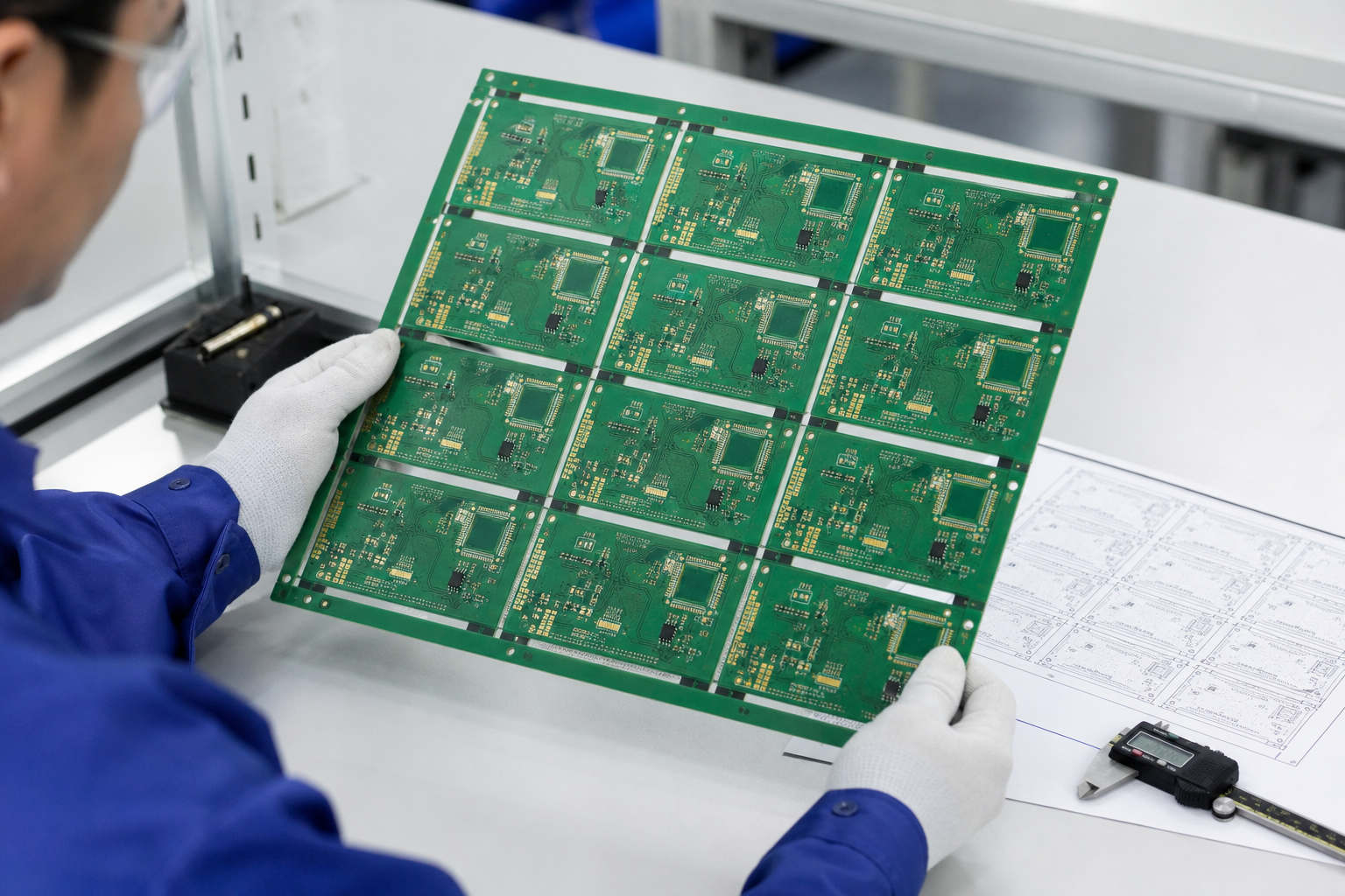
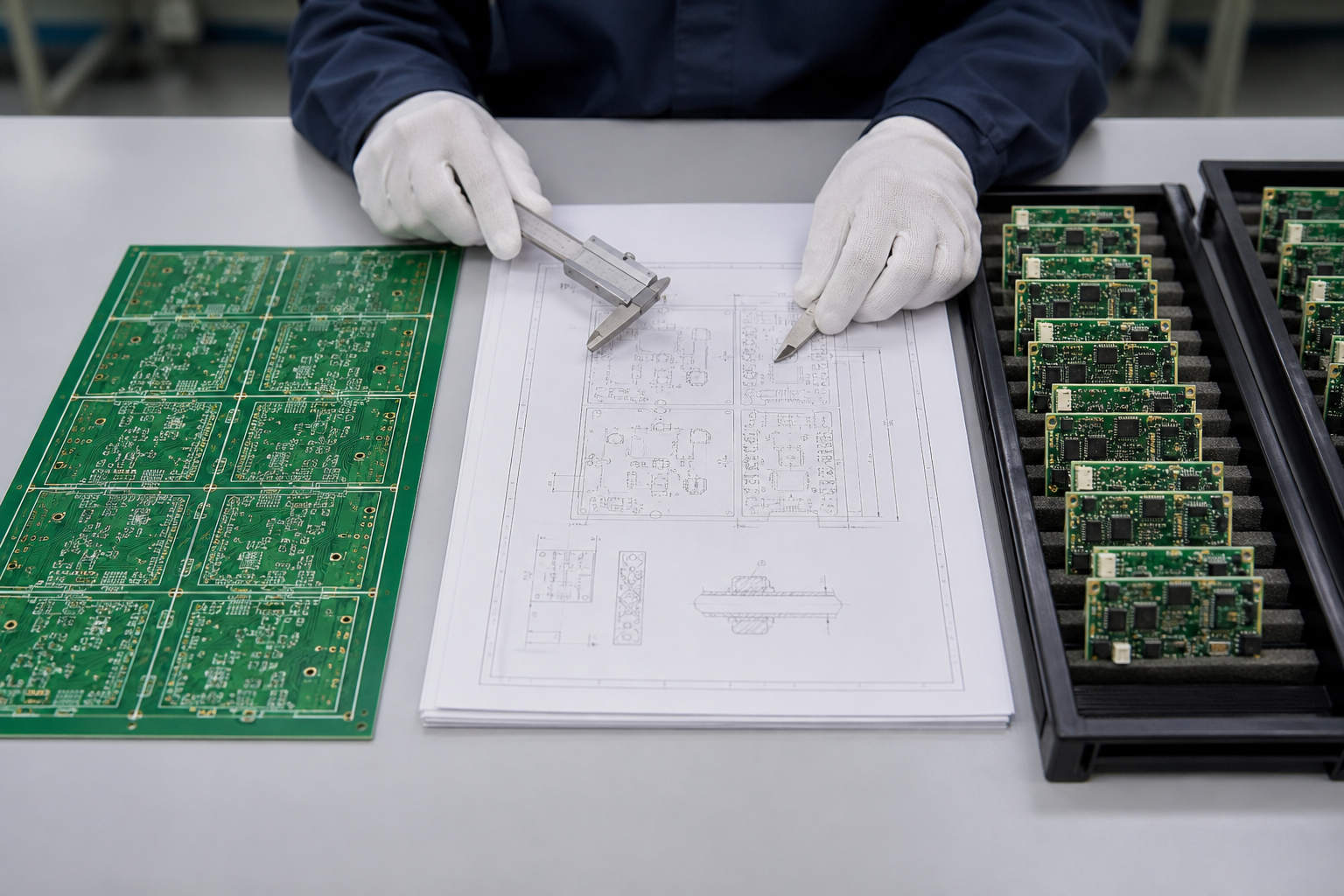
Engineers reviewing PCB board-edge clearance on a production panel
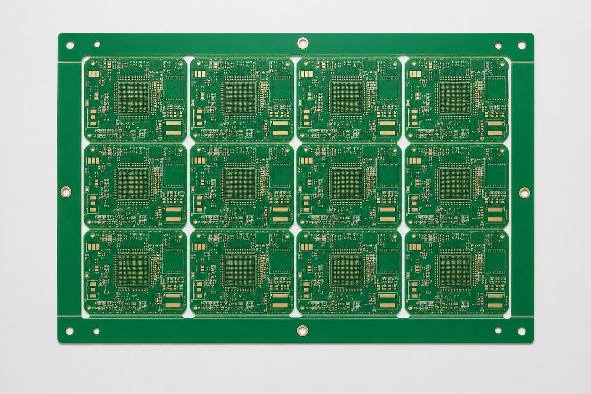
PCB edge clearance must match the actual outline, separation process, enclosure and assembly method.

PCB edge clearance is the controlled distance between the finished board outline and copper, traces, components, holes, slots or other functional features. It protects those features from routing tolerance, V-score intrusion, tab removal, depanelization stress, enclosure interference and handling damage.

There is no single safe distance for every board. The correct keepout depends on what is near the edge and how that edge will be manufactured. A routed contour, V-score line, mouse-bite tab, plated edge and card-edge connector each need different DFM logic.

What PCB Edge Clearance Actually Controls

An edge-clearance rule reserves manufacturing and assembly margin around the final board boundary. The CAD outline is nominal; the finished edge has routing, scoring or breakaway variation. Copper and components must remain functional at the worst allowed result.

Separate rules by feature class. Copper-to-edge protects conductors; component-to-edge protects packages and solder joints; hole-to-edge protects mechanical strength; tooling clearance protects assembly access.

Copper and Traces Near a Routed PCB Edge

Routing removes material with a rotating tool whose path and diameter create a finite manufacturing envelope. Copper placed too close can be exposed, smeared, burred or cut. Inner-layer copper also matters even when it is invisible from the surface.

  • Define the finished outline in one authoritative layer.
  • Check copper on every signal, plane and mechanical layer.
  • Include route tolerance and any bevel or chamfer.
  • Review corners and internal cutouts separately.
  • Flag intentional exposed copper rather than relying on proximity.

Component-to-Board-Edge Clearance

A component needs space for placement, soldering, inspection, handling and the final enclosure—not just a footprint that stays inside the outline. Tall parts, connectors, switches and overhanging packages deserve special checks.

Depanelization can flex the board beside an edge. Solder joints and brittle components placed in that stress zone may crack even if assembly initially passes. Consider package orientation, support tooling and the direction in which tabs or scored rails are separated.

Holes, Slots, and Connectors at the Edge

Mounting holes and slots need enough remaining material to carry their mechanical load. A nominal center distance is not enough; review finished hole/slot size, positional tolerance, edge-process tolerance and the mating hardware.

Edge connectors may intentionally approach or cross the outline. Their fingers, bevel, mask opening and mating envelope should be explicitly defined. Ordinary keepout rules should not silently modify an intentional card-edge feature.

Not sure which edge keepout applies to your panel?

Send the Gerber/ODB++, outline, panel method, component drawing and enclosure constraints. EBest Circuit can review routed, scored and tabbed edges before production.

Routing vs V-Score Edge Keepouts

Edge method Main risk Review focus
Routed contour Tool-path and profile tolerance Copper, holes, cutouts, corner radii
V-score Blade path, residual web and separation stress Components/copper on both board faces
Mouse-bite tab Breakout nibs and local bending Tab placement, perforations and nearby parts
Solid breakaway tab Manual/tool separation load Stress direction and finishing operation
Plated edge Intentional copper exposure/process continuity Layer connection, tabs and keepout exceptions

V-scoring normally follows straight lines and affects both faces. Routing supports complex contours but needs tool access and radius allowances. For a broader comparison, see V-grooves vs tab routing.

Do not measure every keepout from an idealized centerline. For routing, reference the finished profile and its allowed tolerance. For scoring, account for the actual cut path and residual web. At mixed edges, divide the outline into process zones so the CAD rules reflect the local separation method rather than applying one global value.

Mouse Bites, Breakaway Tabs, and Depanelization Stress

Tabs are temporary panel structures, but their removal can permanently damage nearby circuitry. Keep fragile components, small solder joints, ceramic packages and critical traces away from high-strain locations when possible.

Mouse-bite perforations leave small edge remnants that may require finishing. Tab position must also allow depaneling tools and avoid blocking connectors or enclosure surfaces. Review the separated board, not only the intact panel.
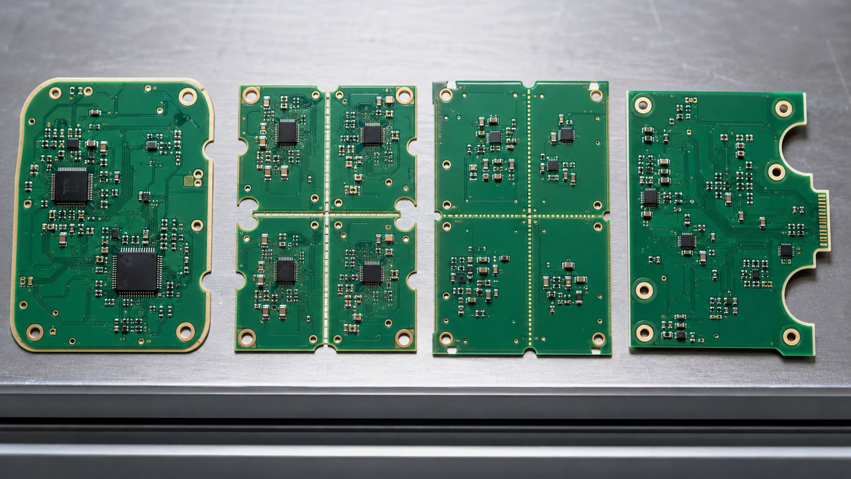
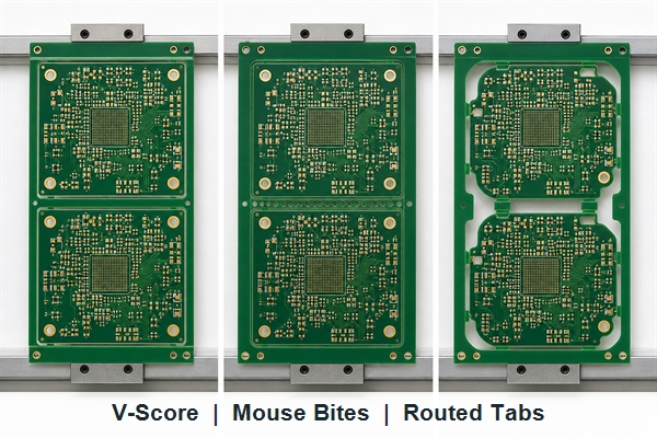
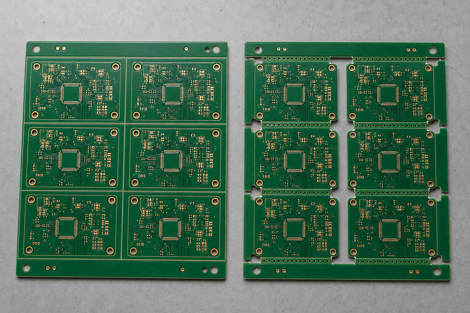
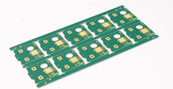
PCB examples with routed scored tabbed and shaped board edges
Edge-processing method changes the mechanical and copper keepout needed around the finished board.

Edge Plating and Card Fingers Are Intentional Exceptions

Edge plating deliberately brings copper to the finished contour, so standard copper keepouts cannot be applied blindly. The fabrication data should define which layers connect, where plating starts/stops and how panel tabs avoid interrupting the plated region.

Review grounding, shielding and connector intent as well as manufacturability. Our PCB edge-plating design guide covers the handoff in detail.

High Voltage and Harsh-Environment Edge Clearance

Electrical clearance to a board edge can be more demanding than basic routing capability. Pollution, moisture, coating strategy, altitude, contamination and enclosure geometry can affect creepage and clearance decisions.

Do not use a generic fabrication keepout as proof of electrical safety. Identify the working voltage, environment, insulation concept and applicable product requirements, then coordinate layout and manufacturing rules.

Assembly Tooling, Conveyors, and Test Access

Assembly may need edge rails, clamps, conveyor contact, selective-solder fixtures or depaneling support. Components or solder joints inside those zones can collide with tooling or prevent stable support.

Share the panel and assembly concept early. A bare-board outline may be manufacturable while the assembled panel is impossible to transport or fixture. Test points and programming connectors near an edge also need probe and cable access.

Board Outline Data and DFM Communication

A clean, closed and uniquely identified outline prevents many edge-clearance errors. Remove duplicate contours, ambiguous construction lines and conflicting dimensions. Define internal cutouts, slots, radii, bevels and controlled edge features.

The panel drawing should show rails, tabs, scores, tooling holes, fiducials and separation notes. If the fabricator may change tab positions, define which component/copper zones are protected and require approval for functional changes.

Compare the bare-board outline with the mechanical enclosure model and the assembled-component body outlines. A connector can satisfy copper keepout while its housing, latch or cable still collides with the case. Likewise, a mounting boss or gasket can overlap a component courtyard even when the PCB profile itself is correct.

Need routing, scoring, and assembly rules reviewed together?

Provide the board outline, panel drawing, BOM/CPL, enclosure and separation method. We can flag conflicts before tooling is released.

PCB Edge-Clearance Checklist Before Release

  1. Confirm the authoritative finished-board outline.
  2. Identify routing, scoring, tabs and intentional plated edges.
  3. Check copper and planes on every layer.
  4. Review components by body, courtyard and assembly access.
  5. Check holes/slots against finished geometry and loads.
  6. Protect brittle parts from depanelization stress.
  7. Include enclosure, connector and keepout envelopes.
  8. Separate electrical-safety spacing from fabrication capability.
  9. Review the assembled and separated board.
  10. Freeze the approved panel revision and deviation process.

What to Send for EBest Circuit Review and Quotation

Send Gerber or ODB++, drill/rout data, fabrication and panel drawings, stackup, BOM, CPL, enclosure constraints, edge-connector details, quantities, assembly requirements, test needs and target delivery.

EBest Circuit can review file consistency and edge-process conflicts before quotation. Specific clearance capability must be confirmed against the selected construction, panel method and approved production route.

PCB Edge Clearance FAQ

What is PCB edge clearance?

It is the reserved distance between the finished board boundary and functional copper, components, holes or other features.

Is component clearance the same as copper clearance?

No. Components add assembly, tooling, enclosure and stress considerations beyond copper fabrication risk.

Does V-scoring need more keepout than routing?

It often needs a different keepout because blade travel and separation stress affect both faces; use the supplier’s process-specific rule.

Can copper touch the PCB edge?

Only when intentionally designed and approved, such as edge plating or card fingers.

Why keep ceramic components away from breakaway tabs?

Local bending during separation can stress brittle bodies and solder joints.

Do internal-layer planes need edge checks?

Yes. Hidden copper can be exposed by routing or violate electrical/mechanical requirements.

How should mounting holes near an edge be reviewed?

Use finished hole size, position, remaining material, load and mating hardware—not center distance alone.

Does the enclosure define component-to-edge clearance?

It contributes a mechanical envelope, but manufacturing and assembly access must also be satisfied.

What outline errors commonly cause problems?

Duplicate/open contours, conflicting layers, missing cutouts and ambiguous score or route lines.

What files are needed for edge-clearance DFM?

Provide board/panel data, outline and rout files, BOM/CPL, enclosure and connector information, quantities and assembly method.

Protect the edge before panelization turns it into a production constraint.

Send your PCB files, panel method, component data and target delivery.

You may also like

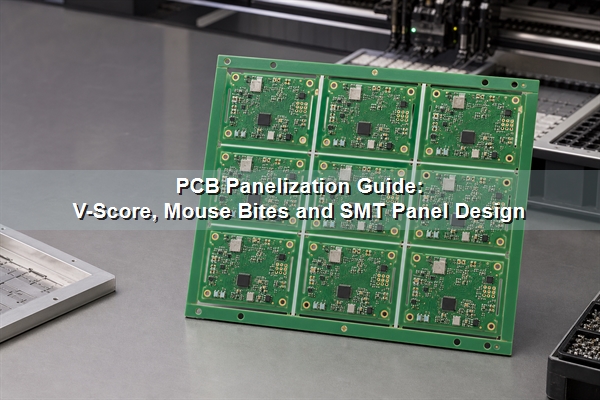
PCB Panelization Guide: V-Score, Mouse Bites and SMT Panel Design
Friday, August 28th, 2026

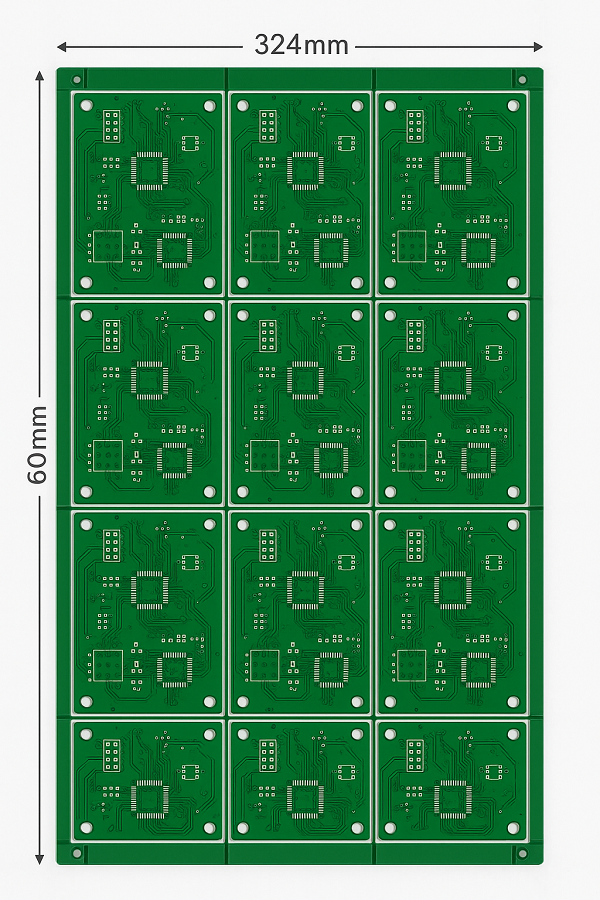
PCB panelization arranges multiple circuit boards within one manufacturing panel so fabrication, solder paste printing, placement, reflow, inspection and handling can process them as a stable unit. A useful panel is not simply the layout that fits the most boards. Its outline, rails, spacing, separation method, tooling features and component clearances must match the fabricator’s CAM rules, the assembly line and the final depaneling process.

PCB panelization guide showing an SMT-ready circuit board array with rails and fiducials

What Is PCB Panelization?

PCB panelization converts one PCB design, or a controlled set of compatible designs, into a larger array that production equipment can transport and process. The finished panel normally includes the repeated board images, panel rails, separation features, global fiducials, tooling holes and identification marks. After assembly and testing, the individual boards are separated by V-scoring, routing, punching, sawing or laser cutting as appropriate.

A single PCB may be large and rigid enough to run without a delivery array, but small, narrow, irregular or thin boards often need added support. The phrase panelization construction is sometimes used for the complete arrangement of boards and temporary panel features. Practical PCB panelization guidelines must therefore define both the customer delivery panel and the fabricator-controlled production panel, which may include several delivery panels plus test coupons.

Why Is Panelizing PCB Important for Fabrication and SMT Assembly?

Panelizing PCB designs reduces repeated handling and gives conveyors, printers, placement machines and inspection systems a consistent rectangular workpiece. Several boards can pass through one stencil print, one placement program and one reflow cycle. Panel rails also protect edge components and create room for machine references that would not fit on a small finished board.

The benefit depends on the whole route. A dense array can improve laminate utilization but become too flexible under stencil pressure. A rigid array may process well yet waste material or impose excessive stress during separation. When the same supplier controls FR4 PCB fabrication and PCB assembly, CAM and SMT engineers can review the delivery panel against fabrication tolerances, stencil data, component placement and depaneling access before release.

Which PCB Panelization Methods Should You Choose?

The separation method should be chosen before the array geometry is frozen. The main PCB panelization methods have different shape, spacing, stress and edge-finish limits.

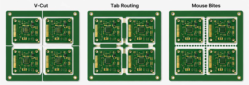
  • V-scoring: uses straight grooves from opposite sides of the panel. It is space-efficient for rectangular boards with continuous straight separation lines.
  • Tab routing: routes most of the board outline while leaving solid tabs. It supports irregular contours and allows the tabs to be cut by a router.
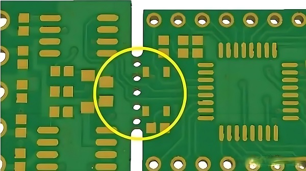
  • Mouse bites: add perforated holes to breakaway tabs for manual separation. A PCB panelization mouse bites pattern must match the fabricator’s drill and routing capabilities.
  • Laser depaneling: provides a narrow, non-contact cut path for suitable materials and thicknesses, but it needs specialized equipment and process review.
  • Punching or sawing: can suit stable high-volume geometries, although tooling cost or straight-line limits restrict their use.

The manufacturer should confirm channel width, residual web, tab placement and keepouts rather than relying on a universal online drawing. Material, finished thickness, copper distribution and component layout all change the result.

PCB panelization methods comparing V-score tab routing mouse bites and routed channels

How Do V-Score and Tab Routing Compare?

The decision starts with board geometry and permitted separation stress. V-score favors straight outlines and high panel utilization. Tab routing accepts complex shapes and controlled tab locations but consumes area for the router path.

Decision factor V-score Tab routing / mouse bites
Board outline Straight, continuous separation lines Curved or irregular outlines are possible
Board spacing Boards may share a score line Routing channel is required
Separation stress Can flex a longer board edge Localized at selected tabs
Finished edge Straight scored edge Tab witness may remain unless machine-routed flush
Component placement Needs clearance from the score and flex zone Needs clearance from tabs, router access and breakout force
Best fit Rectangular, repeatable arrays Irregular shapes and selective support points

For more detail on breakout geometry, see the related guides to mouse bites versus V-groove and V-cut PCB depaneling. The production drawing should still use the dimensions approved for the current manufacturer and equipment.

What Panel Rails, Fiducials and Tooling Holes Are Required?

Panel rails create straight conveyor edges, increase stiffness and hold temporary production features. Their width follows the printer, conveyor, fixture and depaneling setup, not a fixed internet value. Rails may also carry global fiducials, tooling holes, barcodes, coupons and orientation marks.

Global fiducials establish panel translation and rotation for vision-guided equipment. An asymmetric arrangement reduces the chance of loading the panel in the wrong orientation. Tooling holes provide mechanical registration where a fixture or process requires it. Local board fiducials may still be needed near fine-pitch BGA, QFN or other placement-critical packages.

The panel data used to manufacture an SMT stencil must use the same board step-and-repeat, origin and orientation as the placement data. A stencil generated from a single-board paste layer cannot be assumed to match a later CAM-created array unless the duplication and datum transformation are controlled.

PCB panel rails with asymmetric fiducials tooling holes and SMT stencil datum features

How Should PCB Panel Size, Spacing and Component Clearance Be Set?

A reliable PCB panel design starts with the usable machine envelope, then reserves rails, separation geometry and component keepouts before calculating the array count. Filling the entire fabrication sheet first can produce a panel that cannot be printed, transported or depanelized safely.

PCB panel size is constrained by every machine that must handle the panel, including fabrication equipment, stencil printers, pick-and-place systems, reflow conveyors, AOI, test fixtures and depaneling equipment. The smallest and largest usable dimensions, conveyor direction and rail requirements should be confirmed with the actual production route.

Board-to-board spacing follows the separation tool. V-score can place straight board edges together, while routing needs a channel wide enough for the selected cutter and positional tolerance. Laser separation may use a narrower path but requires material and thermal-process review. A PCB panelization calculator can estimate how many boards fit, but it cannot see every process restriction or guarantee the lowest finished-board cost.

Component clearance must include the body, solder joints, overhang, tool envelope and expected board flex. Ceramic capacitors, BGA corners, connectors and heavy parts close to a break line deserve particular attention because depaneling strain can damage a solder joint without leaving an obvious board crack. Copper, vias and controlled-impedance structures also need clearance from score grooves, routed channels and mouse-bite holes.

When Can Different PCBs Share One Panel?

Different PCB part numbers can share a panel only when their fabrication and assembly requirements are compatible. A mixed array generally needs the same material system, layer stack, finished thickness, copper weight, surface finish, solder mask process and production quantity ratio. If one design changes, the shared panel and its assembly data may also require revision.

A homogeneous panel containing one repeated design is easier to control, inspect and replenish. A heterogeneous panel can synchronize a product set and improve material utilization, but it may create unwanted inventory if the demand ratio changes. Rotated boards can improve nesting, yet their copper distribution and component orientation should be checked for reflow, wave soldering and inspection consistency.

Rigid-flex PCB and flex PCB panelization need additional attention to stiffeners, coverlay, bend regions, tooling support and final separation. Their temporary support strategy should be reviewed as part of the material and assembly process rather than copied from a rigid FR4 grid.

What Files Define the Panelization of PCB Arrays?

The panelization of PCB arrays should be defined by one controlled data package. At minimum, identify the finished panel outline, board origins, step-and-repeat, routing or scoring paths, tabs, fiducials, tooling holes, rails and critical dimensions. The fabrication data and the drawing must agree.

  • Gerber or ODB++: copper, mask, legend, profile and panel-level production features.
  • NC drill and rout files: tooling holes, mouse bites, slots and routed channels.
  • PCB panelization drawing: overall dimensions, board arrangement, break features, datums and notes.
  • Pick-and-place data: component coordinates transformed to the panel origin and repeated orientation.
  • Paste and stencil data: the same array count and datum used by assembly.
  • Assembly drawing: panel orientation, board references, special handling and depaneling restrictions.

Do not submit a customer-created panel Gerber together with a single-board NC drill or placement file unless the relationship is explicitly controlled. Mismatched repetition counts, origins and rotations are a common source of preventable CAM and assembly questions.

PCB panelization data review matching Gerber drill panel drawing stencil and placement origins

Which PCB Panelization Software and Tools Are Useful?

A PCB panelization tool is useful for layout exploration, but the correct choice depends on who owns the production data. PCB panelization software inside ECAD can preserve design links; CAM software can duplicate manufacturing layers, drill data and net information; a PCB panelization calculator is best treated as an early utilization estimate.

  • PCB panelization Altium workflows: Embedded Board Array and Draftsman can create repeated arrays and fabrication drawings. Searches for Altium PCB panelization and Altium Designer PCB panelization normally refer to these functions.
  • PCB panelization KiCad workflows: plugins or hierarchical layout methods can create arrays, but users should verify Gerber, drill, position and reference-designator output. The phrase KiCad PCB panelization describes the same task from the tool-first search direction.
  • Fusion 360 PCB panelization: users should confirm whether the selected Electronics/EAGLE workflow exports every required manufacturing and assembly layer for the array.
  • Free PCB panelization software: may be adequate for geometry trials, but output integrity, drill duplication, netlist consistency and revision control still require checking.
  • Manufacturer CAM: usually offers the strongest alignment with actual material utilization, routing tools, panel borders and production equipment.

Software does not know every shop-specific limit. The released files should be checked in an independent CAM viewer and approved against the manufacturer’s panel drawing.

Should You Panelize the PCB or Let the Manufacturer Do It?

Let the manufacturer create the panel when the main goal is cost-efficient fabrication and the array has no product-specific mechanical constraints. Supply clean single-board data, state whether boards must arrive as a panel or separated, identify the assembly route and approve the returned panel drawing. This lets CAM use current working-panel sizes, routing tools and process margins.

Create and control the panel yourself when the assembly fixture, test nest, barcode position, mixed-design ratio, break sequence or customer equipment requires an exact delivery format. In that case, provide both the panel data and the original single-board source, then allow a DFM review. Ownership of the layout does not remove the manufacturer’s responsibility to flag incompatible geometry.

EBest Circuit (Best Technology) lists PCB dimensions up to 610 x 610 mm, subject to stack-up, material, panel utilization and engineering review. The published PCBA process includes 3D SPI, AOI, X-ray and functional testing. Those capabilities are useful only when the approved panel, stencil, placement data and inspection program share the same revision and datum.

How Does PCB Panelization Affect Cost and Yield?

Panelization changes cost through laminate utilization, machine handling, tooling, assembly cycle time, inspection and depaneling. Increasing the number of boards per panel can reduce handling per board, but a weak or warped array can increase paste defects, placement error or breakage. The lowest material scrap is not always the lowest total cost.

Compare layouts using finished good boards per panel, expected yield and all required operations. Include routing time, score setup, tab finishing, carrier or fixture needs, stencil size, test access and the labor or machine time required to separate boards. A mixed array can reduce material waste while increasing data control and inventory risk.

What Must Be Checked Before a PCB Panel Is Approved?

Approval should freeze the panel revision that fabrication, stencil, placement, inspection and test will use. Review the panel drawing and rendered CAM output together rather than approving a dimension table in isolation.

  • Overall panel dimensions, thickness, quantity per panel and conveyor direction are stated.
  • V-score, routing channels, tabs and mouse bites match the intended depaneling process.
  • Rails, fiducials, tooling holes and orientation marks match SMT equipment and fixtures.
  • Components, copper and vias have adequate clearance from every separation feature.
  • Gerber/ODB++, NC drill, stencil, placement and assembly drawings use the same origin, rotation and revision.
  • The panel remains sufficiently rigid through printing, placement, reflow, inspection and handling.
  • Mixed designs share compatible stack-up, materials, finish and production ratio.
  • First-panel separation verifies edge quality, strain-sensitive components and fixture access before volume release.

The related PCB panelization approval guide provides a focused release-control workflow. For the present project, keep the signed panel drawing with the manufacturing package so later revisions cannot silently change the array.

PCB Panelization FAQ

What Is Meant by PCB Panelization?

What is meant by PCB panelization is the temporary grouping of multiple boards into one production unit. The boards remain connected during fabrication or assembly and are separated after the required processes are complete.

Does Every Single PCB Need a Panel?

No. A sufficiently large, rigid and machine-compatible single PCB may run without a delivery array. Small, irregular, thin or edge-sensitive boards usually benefit more from rails and repeated panel processing.

Can a PCB Panelization Calculator Produce Final Manufacturing Data?

It can estimate board count and utilization, but final data still needs routing, score, rail, tooling, fixture and equipment review. Treat the result as a layout proposal rather than automatic production approval.

Can Flex PCB Panelization Use the Same Rules as Rigid FR4?

Not automatically. Flex PCB panelization may use stiffeners, temporary carriers, tooling strips or material-specific separation methods. Bend regions, coverlay and thin-material handling require process-specific review.

Can the PCB Manufacturer Panelize Single-Board Gerbers?

Yes, and this is often the simplest route when the delivery panel has no fixed fixture constraints. State the required panel delivery, assembly process and depaneling preference, then approve the manufacturer’s drawing before production.

Conclusion

Effective PCB panelization connects board geometry with fabrication, SMT handling, separation and data control. Choose the depaneling method first, define rails and machine references, keep every production file on one datum and approve the rendered panel before release. For a DFM review of single-board or controlled panel data, contact EBest Circuit (Best Technology) at sales@bestpcbs.com.

You may also like

PCB Panelization Approval: Prevent Costly Production Changes
Tuesday, August 25th, 2026

A PCB panelization drawing is not just a convenient way to place several boards on one manufacturing panel. It defines how the boards will be fabricated, handled, assembled, separated, counted and delivered. If those decisions are left unclear, a technically correct PCB can still require a new quotation, a revised fixture, manual handling or a last-minute production change.

The practical goal is simple: approve the panel before it becomes a production constraint. This guide helps PCB engineers and buyers decide who should create the array, what the manufacturer needs to review, and which details must be frozen before fabrication and assembly begin.

panelization
Review the PCB panel, production drawing and delivery format before production approval.

What Should Be Confirmed Before PCB Panelization?

Panelization should begin with the required production and delivery flow—not with a target number of boards per panel. Before a panel drawing is created, confirm the following points.

  • Required delivery unit: Will the supplier deliver individual PCBs, complete panels or assembled boards separated after SMT?
  • Single-design or mixed panel: Will every position contain the same design, or must several part numbers share one panel?
  • Quantity basis: Is the order and quotation based on individual pieces or complete panels?
  • Downstream process: Will the panel pass through solder paste printing, pick-and-place, reflow, AOI, functional testing or another fixture-dependent process?
  • Allowed panel changes: May the fabricator rotate boards, change the up count or adjust the rails to improve manufacturability?
  • Depaneling responsibility: Will separation occur at the PCB factory, PCBA factory or customer site?
  • Quality rules: Are X-outs allowed? Are panel-level traceability, coupons, electrical testing or special packaging required?

These answers create the design boundary. Without them, two suppliers can interpret the same Gerber package differently and return quotations that do not cover the same deliverable.

The board construction also matters. A standard FR4 PCB may allow several practical layouts, while a thin flexible circuit, brittle ceramic substrate, heavy-copper board or impedance-controlled multilayer design can impose additional handling and process limits.

Who Should Control the Panelization Design?

Who should control the layout depends on the equipment and downstream processes the panel must fit.

Let the PCB manufacturer create the panel when:

  • You are supplying a single-board Gerber package.
  • The main objective is manufacturability and material utilization.
  • No customer-owned pallet, stencil or assembly fixture fixes the panel dimensions.
  • The manufacturer may adjust rails, spacing and orientation within agreed limits.

In this situation, send the finished board data and the required delivery conditions. The fabricator can propose a production panel based on its process and working-panel format. You should still review the production drawing before release.

Supply or control the array when:

  • A stencil, carrier, test fixture or automated line already depends on a fixed outline.
  • Several different boards must be delivered as one matched set.
  • Board orientation is controlled by a connector, sensor, coating or assembly requirement.
  • The panel must match an approved repeat-order configuration.
  • Traceability or packaging is managed at panel level.

The safest handoff is a documented division of responsibility. The customer defines the functional and downstream constraints, while the manufacturer confirms that the proposed panel can be fabricated, assembled and separated without creating avoidable risk.

Do not assume that an old panel should automatically be reused. A change in laminate, copper weight, board thickness, component placement, assembly site or delivery format can make the previous array unsuitable even when the circuit revision appears minor.

How Should PCB Panelization Methods Match the Board?

The best separation method is the one that fits the board outline, component layout, material and downstream handling—not simply the least expensive cutting process.

  • V-scoring is usually considered when boards have straight shared edges and can be arranged in rows. It can support efficient separation, but the score line and remaining web must be reviewed against board thickness, copper distribution and nearby components. Components, solder joints and brittle features should not be placed where bending during separation can transfer damaging stress.
  • Tab routing is useful for irregular outlines or layouts that cannot share continuous straight edges. Routed gaps define most of the finished profile, while tabs keep each board connected to the array. Tab position, width and removal method should be agreed before production. Poorly positioned tabs can leave difficult edge cleanup or transfer force toward sensitive areas.
  • Mouse-bite perforations can make manually removed tabs easier to break, but hole size, pitch and distance from the finished edge affect the remaining witness marks. If the enclosure requires a smooth edge, secondary finishing or a different tab strategy may be needed.
  • Mixed-design panels may reduce handling for matched products, but they require additional control. The designs must be compatible in material, thickness, copper build, surface finish, process route and delivery quantity. Combining unrelated boards only to fill open space can complicate fabrication, assembly and quality disposition.

Special constructions require more than a generic rectangular array:

  • A rigid flex PCB may need temporary support and careful control of the flexible areas.
  • A ceramic PCB is brittle, so separation force and edge damage need particular attention.
  • Heavy-copper and asymmetrical multilayer boards may require warpage review.
  • Thin boards and FPCs may depend on tooling or carriers for stable assembly handling.
  • Impedance-controlled boards require the approved stackup and coupon strategy to remain aligned with the production panel.

This is why PCB panelization methods should be selected after the manufacturer reviews the actual build—not copied from a visually similar board.

panelization
V-scoring and routed breakaway tabs must match the board outline, material and separation requirements.

How Do PCB Panel Size and Array Quantity Affect Cost?

More boards per panel do not automatically mean a lower total cost. The better question is whether the selected PCB panel size creates a stable, repeatable route through fabrication and assembly.

The real panel cost is influenced by:

  • The usable manufacturing area and required process margin.
  • Board outline, rotation and spacing.
  • Rail width and routing channels.
  • Tooling holes, fiducials, coupons and identification areas.
  • Material type, copper weight, layer count and stackup.
  • Fabrication yield and the policy for defective units within a panel.
  • SMT line limits, stencil dimensions and fixture size.
  • Whether the supplier ships by piece or by complete panel.

For example, increasing an array from four boards to six may improve laminate utilization, but it can also make the panel less rigid, exceed an assembly-line limit or increase the commercial impact of one rejected panel. Conversely, an array with generous unused space may be justified when it provides the rails, support and keep-outs required for stable processing.

Buyers should request a quotation that states:

  • Finished board size.
  • Proposed panel size.
  • Number of boards per panel.
  • Number of panels and total good-board quantity.
  • Whether X-outs are permitted.
  • Whether the price includes depaneling.
  • Whether assembly and final delivery are quoted per panel or per finished board.

This removes a common source of price confusion: two quotations may show the same piece quantity while assuming different panel counts, separation work or acceptable panel yield.

How Should Panel Design Support Assembly and Depaneling?

A fabrication-efficient array can still be inconvenient for PCBA. The panel should be reviewed as a temporary production tool that must remain stable from solder paste printing through final separation.

For automated assembly, check:

  • Rails provide sufficient support for conveyors and board handling.
  • Global fiducials and tooling holes match the assembler’s requirements.
  • Component orientation supports the intended process flow.
  • Edge components, connectors and overhanging parts have enough clearance.
  • The panel remains sufficiently rigid through printing, placement and reflow.
  • Barcode, serial-number and traceability locations remain accessible.
  • Test points and fixtures can reach the required locations.

For depaneling, check:

  • Score lines or tabs do not intersect copper, plated features or sensitive areas.
  • Tall, heavy, ceramic or brittle components are kept away from high-stress separation zones.
  • The selected tool can access every separation path.
  • Edge quality is suitable for the enclosure or mechanical interface.
  • The separated board can be handled and packaged without damaging protruding parts.

If one supplier handles both PCB fabrication and prototype PCB assembly, the panel can be reviewed against the real SMT flow before the first build. The customer retains final approval, while the combined review reduces handoff gaps between a fabrication-only drawing and the assembly process that follows.

panelization
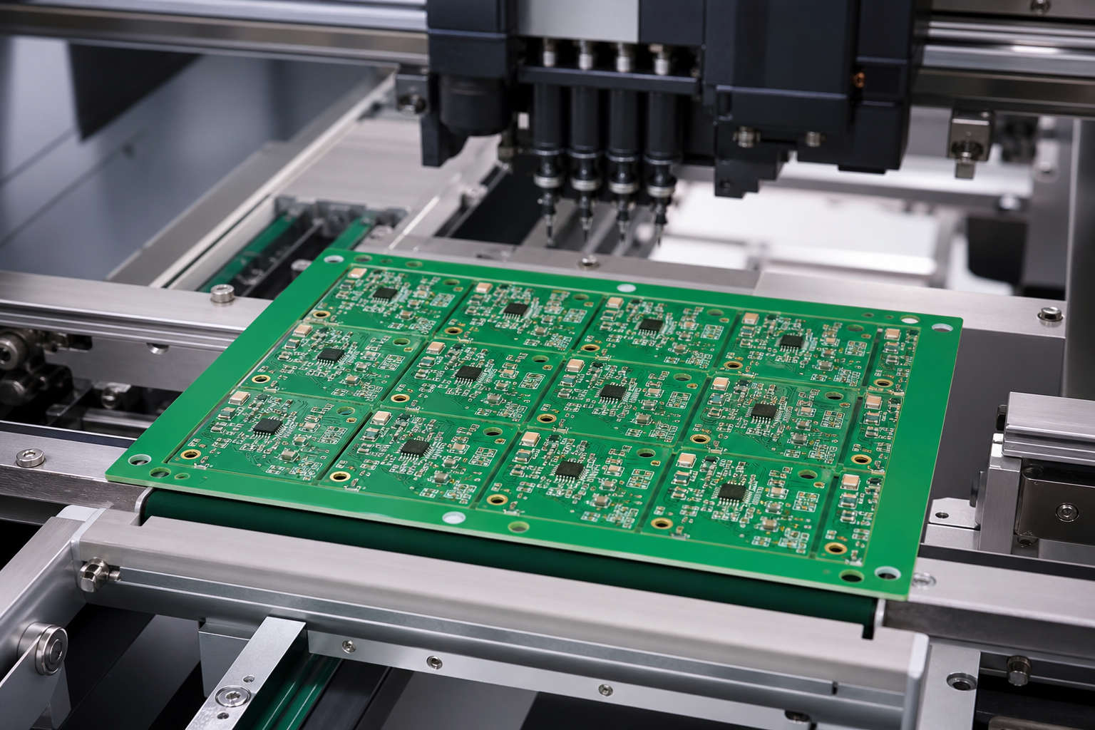
Tooling rails, fiducials and panel rigidity help the array move reliably through SMT assembly.

What Should Be Reviewed Before Production Approval?

The production panel drawing should turn assumptions into visible, reviewable requirements. Before approval, compare it with the released board files, assembly information and purchase requirements.

Review at least these items:

  • Revision identity: Board part number, revision and file date match the released package.
  • Finished outline: Board dimensions, slots, cutouts and critical tolerances are correct.
  • Array definition: Panel dimensions, up count, orientation and mixed-board arrangement are identified.
  • Separation features: V-scores, routed gaps, tabs and mouse bites are dimensioned and correctly located.
  • Manufacturing rails: Rail width, tooling holes, fiducials, coupons and markings are included where required.
  • Component clearance: Assembly keep-outs and edge-component risks have been checked.
  • Stackup and material: Thickness, laminate, copper build and impedance requirements match the approved construction.
  • Quality disposition: X-out rules, test requirements and acceptance criteria are recorded.
  • Delivery format: Panel delivery, individual-board delivery or post-assembly separation is stated.
  • Packaging and traceability: Panel quantity per package, labels, date codes and protective packaging are defined.

Record technical questions and answers in a controlled engineering-query log. If the fabricator changes the up count, orientation, score position, tooling rail or stackup, the revised drawing should be approved before production rather than accepted through an informal message.

For repeat orders, confirm that the approved panel revision still matches the current PCB, BOM, assembly drawing and delivery requirement. A previously manufactured panel is useful evidence, but it is not a substitute for revision control.

PCB Panelization Case Study: From Panel Approval to Assembly

A two-layer PCB project shows why panel approval must cover fabrication, assembly and final delivery—not just the number of boards in an array.

The project used a two-layer PCB with 370HR material, 1.5 oz copper, a finished thickness of 1.57 mm with tolerance, ENIG and IPC Class 3 requirements. The fabrication record also specified plugged vias, identification markings and electrical testing.

The important panelization decision was not simply how many boards could fit on a working panel. The documented production flow required:

  • The blank-board manufacturer to create the production panel.
  • The production panel drawing and stackup to be sent for customer confirmation.
  • Bare PCBs to be electrically tested before assembly.
  • Bare boards to be delivered in panel form for lead-free SMT.
  • Finished assemblies to be separated and delivered as individual boards.
  • Final assembled boards to use antistatic packaging.

This sequence created three different definitions that had to remain consistent: the individual PCB design, the fabrication panel and the post-SMT delivery unit. If the quotation had stated only the number of individual boards, it would not have fully described the required work.

The approval review therefore needed to verify the panel outline, rails, fiducials, tooling provisions, up count, stackup, assembly handling and final separation responsibility. The value came from connecting fabrication data with assembly and delivery requirements before production began, instead of treating panelization as an isolated CAM step.

For buyers, the practical lesson is to approve the full route—not only the Gerber image. A panel is temporary, but the decisions built into it affect every board passing through the line.

panelization
Panel approval connects bare-board fabrication, assembly handling and individual-board delivery.

FAQs About PCB Panelization

Should I include a panelized Gerber file when requesting a quotation?

You may provide one when a fixed array is required, but also include the single-board Gerber data and clearly identify which file controls production. If no fixture or downstream constraint fixes the array, sending the single-board data plus your delivery requirements allows the manufacturer to propose a manufacturable panel.

Can a PCB manufacturer change my panelization design?

The manufacturer may recommend changes to spacing, rails, tooling features, orientation or separation details. No production-affecting change should be assumed automatically. The proposed production drawing and any engineering questions should be reviewed and approved through revision control.


Is V-scoring always cheaper than tab routing?

Not in every project. V-scoring can be efficient for boards with compatible straight edges, while routed tabs suit many irregular outlines. The total cost also depends on material utilization, routing time, assembly handling, edge-quality requirements and the selected depaneling process.

Can different PCB designs be placed on the same panel?

Yes, when the designs and manufacturing routes are compatible. Material, thickness, copper build, surface finish, process steps, assembly requirements and quantities must be reviewed together. A mixed panel should solve a production or delivery need, not merely fill unused space.

What files are needed for a panelization review?

Send the released single-board Gerber or ODB++ package, NC drill data, fabrication drawing, stackup and impedance requirements. For assembled products, also send the BOM, centroid or pick-and-place file, assembly drawings, component height information, required delivery format and any stencil, pallet, fixture or test constraints.

Before approving your next panel, send EBest Circuit (Best Technology) the released PCB files, assembly requirements and intended delivery format. You work with one dedicated sales contact backed by three engineers, giving you one communication channel for manufacturability review, PCB fabrication, component sourcing and PCBA assembly. For a panelization and DFM review, contact sales@bestpcbs.com.

Confirm the PCB panelization route before production so the quotation, fabrication panel, SMT process and final delivery unit describe the same product.

You may also like

PCB Panel Sizes Explained: How to Maximize Board Yield and Reduce Manufacturing Cost
Wednesday, August 5th, 2026

PCB panel sizes are not governed by one universal standard. An 18 Ɨ 24 in fabrication panel is a common reference, while an SMT assembly panel is usually smaller and must fit every machine in the line. The right size depends on usable area, board dimensions, rails, spacing, depaneling, rigidity, and equipment limits.

This distinction matters because the sheet purchased by a fabricator, the area available for nesting boards, and the panel delivered to an assembly line are not necessarily the same size. A panel that looks efficient in CAD can still fail at the stencil printer, sag in reflow, or leave insufficient clearance for depaneling. Use the following framework to compare common PCB panel sizes before approving the array.

PCB panel sizes shown on a production-ready circuit board array

What Are the Most Common PCB Panel Sizes?

There is no single standard PCB panel size used by every fabricator and assembler. The PCB panel sizes below are practical references seen in fabrication and assembly planning. They are starting points—not guaranteed machine limits or a substitute for supplier confirmation.

Panel reference Approximate inches Typical planning role Important limitation
250 Ɨ 250 mm 9.84 Ɨ 9.84 in Compact assembly array or smaller fabrication format Usable area is smaller after rails and process margins
250 Ɨ 300 mm 9.84 Ɨ 11.81 in Compact SMT panel reference Must fit the narrowest machine and conveyor setting
300 Ɨ 400 mm 11.81 Ɨ 15.75 in Medium assembly or fabrication reference Rigidity depends on thickness, cutouts, copper, and support
400 Ɨ 500 mm 15.75 Ɨ 19.69 in Larger-format planning reference May be too large for some SMT lines or fixtures
457 Ɨ 610 mm 18 Ɨ 24 in Widely referenced fabrication panel Full sheet dimensions do not equal usable nesting area
508 Ɨ 610 mm 20 Ɨ 24 in Alternative fabrication format Availability and processing rules vary by supplier
610 Ɨ 914 mm 24 Ɨ 36 in Large raw-material or fabrication reference Usually subdivided before assembly handling

The best reference size is the one that creates a manufacturable array with acceptable yield, stable handling, and a clean depaneling path. Ask whether a quoted dimension describes raw laminate, a fabrication working panel, or the finished delivery array.

Fabrication Panel vs Usable Area vs SMT Assembly Panel

PCB panel sizes can describe four different objects. Confusing them is one of the most common causes of incorrect yield estimates.

Panel term Purpose Main constraint What to confirm
Raw or full fabrication panel Starting laminate or working sheet Fabrication equipment and material format Whether quoted dimensions are raw or process-ready
Usable fabrication area Area available for boards and required features Process margins, coupons, tooling, and routing space Confirmed usable width and height
Customer array or delivery panel Multiple boards shipped together Array count, rails, depaneling, packing, and handling Overall dimensions and delivery condition
SMT assembly panel Carrier through printing, placement, reflow, AOI, and test The narrowest handling window across the line Minimum, maximum, thickness, rail, and support requirements

A fabricator may optimize several customer arrays within one working panel, but the assembler only handles the delivery panel. This is why PCB fabrication panel size and PCB assembly panel size should be checked separately.

Full PCB Panel Size vs Usable Panel Area

When comparing PCB panel sizes, usable panel area is the full panel area minus process margins and reserved zones. A simple first-pass model is:

Usable width = full width āˆ’ left margin āˆ’ right margin
Usable height = full height āˆ’ top margin āˆ’ bottom margin

Margins may contain tooling holes, global fiducials, impedance coupons, plating thieving, test structures, barcodes, or gripping zones. Router paths and breakaway rails also consume space. Therefore, an 18 Ɨ 24 PCB panel does not provide a universal 18 Ɨ 24 in usable area.

For example, if an 18 Ɨ 24 in working panel requires a 0.5 in reserved zone on each side, the simplified usable rectangle becomes 17 Ɨ 23 in. This is only a calculation example; actual process margins must come from the fabricator. Complex routing, coupons, or process constraints may reduce the usable region further.

Top-down PCB panel showing the array, edge rails, tooling holes, and usable area

How to Calculate PCB Panel Size and Boards per Panel

Calculate both board orientations before choosing among PCB panel sizes. Let the usable panel dimensions be Uw and Uh, board dimensions be Bw and Bh, and the required gap between boards be G.

Columns = floor((Uw + G) Ć· (Bw + G))
Rows = floor((Uh + G) Ć· (Bh + G))
Boards per panel = columns Ɨ rows

Worked example. Assume a 300 Ɨ 400 mm delivery panel with 10 mm rails on all four sides. The simplified usable area is 280 Ɨ 380 mm. The single board is 70 Ɨ 95 mm, and the selected routing strategy requires a 2 mm gap.

  • At 0°: floor((280 + 2) Ć· (70 + 2)) = 3 columns; floor((380 + 2) Ć· (95 + 2)) = 3 rows; total = 9 boards.
  • At 90°: floor((280 + 2) Ć· (95 + 2)) = 2 columns; floor((380 + 2) Ć· (70 + 2)) = 5 rows; total = 10 boards.
  • Board-area utilization for the 2 Ɨ 5 option is (10 Ɨ 70 Ɨ 95) Ć· (300 Ɨ 400) = 55.4% of the full delivery-panel area.

The rotated layout fits one more board, but quantity is not the only approval criterion. The 2 Ɨ 5 array must still pass checks for rail direction, conveyor support, component orientation, copper balance, tooling access, and depaneling stress. If it becomes long and flexible, the 3 Ɨ 3 option may be safer despite its lower count.

Minimum and Maximum PCB Panel Size Across the SMT Line

The minimum and maximum PCB panel sizes for assembly are set by the complete line, not by one machine in isolation. Check the stencil printer, loader, conveyor, pick-and-place machine, reflow oven, AOI, ICT or FCT fixture, depaneling equipment, and any manual carriers. The smallest maximum—or the largest minimum—becomes the controlling limit.

  • Too small: the board may not clamp, convey, or expose enough edge area for fiducials and tooling.
  • Too large: the panel may exceed a transport window, fixture, stencil format, or safe manual-handling range.
  • Too flexible: a nominally acceptable panel may sag during printing, placement, or reflow.
  • Too heavy: dense components or metal structures may overload support assumptions.

BestPCBS separates standard-process dimensions from special-process review in its controlled PCB Manufacturing Capability data. The following values describe confirmed finished-board and V-cut capabilities; they are not universal industry standards and do not replace a project-specific panel review.

Confirmed capability item Standard process Special process or review condition
Finished board maximum dimension Within 600 mm Single/double-sided FR-4: 600–1980 mm; multilayer FR-4: 600–750 mm
Finished board minimum dimension 5 mm A single side of 5–10 mm is shipped by panel
Minimum distance between two V-cut lines 8 mm Array interaction requires engineering confirmation
V-cut board thickness range 0.6–3.5 mm More than 4 mm requires a special process
Minimum trace-to-board-edge distance for V-cut or routing 8 mil Component and mechanical clearances still require DFM review

A PCB can be fabricable yet unsuitable for an SMT line, so the finished delivery panel must be approved against assembly equipment as well as fabrication capability.

How Rails, Board Spacing, Tooling Holes, and Fiducials Change Panel Dimensions

Every handling feature uses panel area. Add these features before calculating final yield, not after the array count has been fixed.

Design element Why it is used Effect on dimensions Who confirms it
Edge rails Conveyor support, clamping, fiducials, and edge clearance Increase overall width, height, or both Assembler with fabricator review
Board spacing Allows scoring, routing, tabs, and safe separation Accumulates between every row and column Fabricator based on depaneling method
Tooling holes Locates the panel in fixtures and processes Requires reserved rail or margin area Assembler and fixture owner
Global fiducials Aligns the complete panel for printing and placement Requires clear optical zones, usually on rails Assembler
Local fiducials Improves alignment for fine-pitch devices or individual boards Uses board-level surface area PCB and assembly engineers
Coupons and labels Supports process control, traceability, or testing Consumes fabrication or rail space Fabricator and quality team

A complete panel drawing should identify the overall dimensions, board array, rails, board spacing, score or router path, tabs, tooling holes, fiducials, orientation, coupon area, barcode zone, and bad-board marking method. Do not assume one tooling-hole or rail dimension works for every production line.

V-Score vs Tab Routing: How the Method Changes Panel Size

V-scoring suits straight, continuous separation lines and regular rectangular arrays. Tab routing supports irregular outlines and selective separation, but it needs router clearance, tabs, and often mouse-bite finishing. The method changes both the required spacing and the residual stress at the board edge.

Decision factor V-score Tab routing
Board outline Best for straight shared edges Works with curves and irregular shapes
Spacing Can support closely arranged straight edges, subject to process rules Needs a router path plus tab locations
Edge result Leaves a scored separation edge May leave tab or mouse-bite witness marks
Component risk Board bending during separation can stress nearby parts Tab cutting can reduce bending but needs tool clearance
Panel rigidity Long score lines can weaken the array Tab number and placement control stiffness

Minimum and maximum V-cut panel size are supplier- and equipment-specific. Confirm V-cut line spacing, board thickness, component clearance, scoring direction, and permitted edge condition before finalizing the panel.

How Board Thickness, Weight, and Copper Balance Affect Panel Stability

A larger panel is not automatically more economical. Thin laminates, long unsupported spans, large cutouts, asymmetric copper, heavy components, and too few connecting tabs can produce sag or twist. That movement can affect solder-paste release, placement height, reflow support, AOI focus, and depaneling.

Request engineering review when the panel combines two or more risk factors: a long aspect ratio, thin construction, dense copper on one side, heavy connectors, large routed openings, components close to break lines, or narrow rails. Possible responses include changing orientation, reducing the array, widening rails, adding temporary support, balancing copper, repositioning tabs, or using a carrier.

PCB assembly panel moving through an SMT production line with supported edge rails

How PCB Panel Size Affects Material Utilization and Cost

The economics of PCB panel sizes include more than laminate area. Cost can be affected by the number of boards per working panel, routing time, wasted edge strips, rail area, tooling, stencil and fixture compatibility, assembly handling, test access, depaneling labor, and the risk of damaging multiple boards at once.

A high-count array may look attractive but lose its advantage if it needs a custom carrier, slows handling, or increases breakaway damage. Compare at least two orientations and, where practical, two delivery-panel sizes. For a realistic quotation, pair the proposed layout with the quantity and process data described in a custom PCB cost guide.

The useful target is not maximum geometric utilization. It is the lowest stable cost per acceptable board after fabrication, assembly, test, and depaneling constraints are included.

How to Choose the Right PCB Panel Size

  1. Confirm the exact single-board outline, thickness, stack-up, copper weight, and edge-mounted components.
  2. Ask the fabricator for its working-panel formats, confirmed usable area, process margins, and relevant special-process limits.
  3. Ask the assembler for the minimum and maximum handling dimensions of every machine and fixture in the line.
  4. Select V-score, tab routing, or another approved separation method based on outline, edge quality, and component stress.
  5. Add rails, board gaps, fiducials, tooling holes, coupons, and traceability zones.
  6. Calculate both 0° and 90° layouts, including the spacing between every row and column.
  7. Review stiffness, copper balance, component weight, conveyor support, and depaneling forces.
  8. Approve one controlled panel drawing with the fabricator and the provider of custom PCB assembly services.

Early joint review prevents the common handoff problem in which a fabrication-efficient panel has to be rebuilt for SMT. It also gives both suppliers one agreed definition of the overall panel dimensions and usable area.

What Information Should You Send for PCB Panel Review?

Send enough information for the fabricator and assembler to evaluate the same panel—not separate assumptions.

  • Gerber, ODB++, IPC-2581, or another reviewable PCB data package
  • Board outline, single-board dimensions, thickness, stack-up, and copper weight
  • Required board quantity per delivery panel, or permission to optimize the array
  • Assembly side, component overhang, edge clearance, and process flow
  • V-score or tab-route preference and the required finished edge
  • Rail, fiducial, tooling-hole, barcode, coupon, and bad-board marking requirements
  • Delivery condition: individual boards, bare-board panels, or assembled panels
  • Order quantity, test method, fixture constraints, and depaneling responsibility

If no customer array is mandatory, submit the single-board production files and ask the fabricator to propose a panel for joint DFM approval. That approach is often safer than locking dimensions before the SMT line and separation method are known.

FAQs About PCB Panel Sizes

Q1. Is there one universal standard PCB panel size?

A1. No—there is no universal panel size. Common dimensions are planning references. Each fabricator and assembler has its own material formats, process margins, equipment windows, and preferred arrays. Confirm whether a stated size means a raw sheet, usable fabrication area, or delivery panel.

Q2. How many PCBs fit on an 18 Ɨ 24 inch panel?

A2. The count depends on usable area and layout rules. Subtract fabrication margins, rails, coupons, router paths, and required spacing, then calculate both board orientations. Board outline, depaneling method, and process support can make the highest geometric count unsuitable.

Q3. Do panel rails count toward the overall PCB panel dimensions?

A3. Yes—rails are normally included in the delivered panel dimensions. They consume space but provide conveyor support, clamping area, tooling locations, and global fiducials. State both the overall panel size and the internal array size on the drawing.

Q4. What is the minimum PCB panel size for SMT assembly?

A4. The assembly line determines the practical minimum. A small board may need rails or a multi-board array so the printer, conveyor, placement machine, reflow oven, and inspection equipment can grip and transport it reliably.

Q5. What is the maximum V-cut PCB panel size?

A5. There is no universal maximum V-cut size. The limit depends on the supplier’s scoring equipment, material, thickness, score direction, panel rigidity, and downstream assembly line. Obtain a project-specific confirmation instead of applying another supplier’s published number.

Q6. Should I panelize the PCB myself or let the manufacturer do it?

A6. Let the manufacturer optimize it unless your assembly line requires a controlled array. If you provide the panel, have both fabrication and assembly teams review it. Never assume a CAD array is production-ready without checking tooling and depaneling.

Q7. When should small or prototype PCBs be panelized?

A7. Panelize when individual handling is unreliable or inefficient. Very small boards often need rails or an array for solder-paste printing, placement, reflow, inspection, or test. For low quantities, balance easier handling against panel setup and depaneling work.

Q8. Can different PCB designs share one panel?

A8. Mixed-design panels are possible only with supplier approval. Different outlines, copper distribution, layer constructions, quantities, and test requirements can complicate fabrication and assembly. Confirm fabrication rules, traceability, bad-board handling, and order acceptance before nesting different designs.

Q9. Does rotating boards reduce PCB panel cost?

A9. Rotation can improve yield, but it does not always reduce total cost. A rotated layout may fit more boards yet create poor conveyor support, unfavorable grain or copper behavior, awkward component orientation, or greater depaneling risk. Compare the complete process.

Q10. What panel files should be approved before production?

A10. Approve one dimensioned panel drawing and its production data. The package should show the array, overall size, rails, gaps, score or router paths, tabs, fiducials, tooling holes, orientation, labels, coupons, and bad-board marking requirements.

Conclusion

PCB panel sizes should be chosen by working backward from usable fabrication area, assembly-line handling, depaneling, and mechanical stability. Common PCB panel sizes provide a useful starting point, but the approved panel must reflect the actual board, process, and supplier limits. Calculate both orientations, include every rail and gap, and have fabrication and assembly review the same controlled drawing.

Send your Gerber files, board outline, assembly side, quantity, and preferred delivery format to sales@bestpcbs.com for a DFM panel review.

You may also like

Common PCB Panel Sizes: From Board Dimensions to Panel Design
Wednesday, June 17th, 2026

Common PCB panel sizes play an important role in PCB manufacturing cost, material utilization, SMT assembly efficiency, and final board quality. Choosing the right PCB panel size can help reduce material waste, improve production yield, and make assembly more stable. Whether your project uses small boards, irregular PCB shapes, V-cut panels, or tab-routed designs, understanding common PCB panel sizes helps you plan the panel layout more clearly before manufacturing.

EBest Circuit provides one-stop PCB manufacturing and assembly services, including DFM review, PCB panel design support, quick PCB prototyping, SMT assembly, functional testing, and full turnkey PCBA service. Our engineering team can help review Gerber files, BOMs, panel drawings, tooling holes, fiducial marks, V-cut lines, and tab routing requirements before production. If you need support with PCB panel size selection, panelization, or assembly preparation, you can contact us at sales@bestpcbs.com.

Common PCB Panel Sizes

What Are Common PCB Panel Sizes?

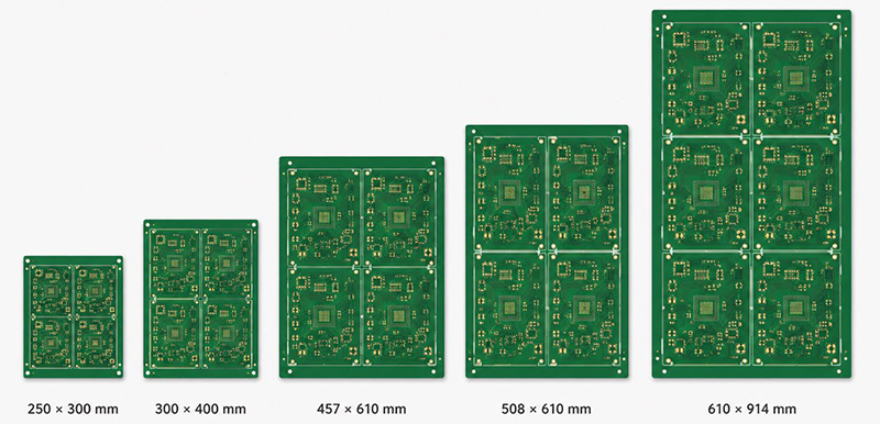
Common PCB panel sizes are not fixed universal standards. However, many PCB manufacturers use reference sizes such as 250 Ɨ 300 mm, 300 Ɨ 400 mm, 457 Ɨ 610 mm, 508 Ɨ 610 mm, and 610 Ɨ 914 mm.

In inches, common PCB fabrication panel sizes include 18 Ɨ 24 in, 20 Ɨ 24 in, and 24 Ɨ 36 in. For SMT assembly, medium panel sizes such as 250 Ɨ 300 mm and 300 Ɨ 400 mm are often easier to handle and more suitable for production equipment.

The right PCB panel size depends on the single PCB board dimensions, usable panel area, material utilization, SMT machine limits, V-cut or tab routing method, tooling holes, fiducial marks, and depanelization requirements.

Common PCB Panel Sizes

Why PCB Panel Sizes Matter?

PCB panel size affects cost, yield, assembly efficiency, and manufacturing stability. A well-designed panel allows multiple PCB units to be processed together instead of being handled one by one.

A proper PCB panel size can help:

  • Improve material utilization
  • Reduce PCB fabrication cost
  • Increase the number of boards per production run
  • Improve SMT assembly efficiency
  • Reduce handling damage
  • Make solder paste printing more stable
  • Support faster inspection and testing
  • Reduce production errors during depanelization

Panel size also affects communication with the PCB manufacturer. If the panel is too large, it may bend, warp, or exceed equipment limits. If the panel is too small, it may be difficult to handle during SMT assembly.

This is why common PCB panel sizes should be treated as engineering references, not as fixed standards for every project.

Common PCB Panel Sizes Chart in mm and Inches

The following chart shows common PCB panel sizes in both mm and inches. These sizes are useful for early design planning, cost estimation, and communication with PCB manufacturers.

Panel TypeSize in mmSize in inchesCommon Use
Small panel250 Ɨ 250 mm9.84 Ɨ 9.84 inPrototype / small PCB
SMT panel250 Ɨ 300 mm9.84 Ɨ 11.81 inSmall to medium PCBA
Standard SMT panel300 Ɨ 400 mm11.81 Ɨ 15.75 inGeneral assembly
Large SMT panel400 Ɨ 500 mm15.75 Ɨ 19.69 inHigher unit count
Fabrication panel457 Ɨ 610 mm18 Ɨ 24 inFactory working panel
Fabrication panel508 Ɨ 610 mm20 Ɨ 24 inLaminate-based production
Large fabrication panel610 Ɨ 914 mm24 Ɨ 36 inLarge production panel

One important point is that overall panel size is not the same as usable panel area.

For example, an 18 Ɨ 24 inch fabrication panel does not mean the full area can be used for PCB units. Some space may be reserved for tooling holes, test coupons, process margins, routing clearance, panel rails, and handling requirements.

So when you discuss PCB panel size with a manufacturer, ask two questions:

  • What full panel sizes do you support?
  • What usable panel area is available for my design?

This helps avoid layout mistakes before fabrication or assembly begins.

What Is a PCB Panel?

A PCB panel is a larger board that contains multiple individual PCB units arranged together for fabrication or assembly. This process is called PCB panelization.

A PCB panel may include:

  • PCB units
  • Process rails
  • V-cut lines
  • Tab routing bridges
  • Mouse bites
  • Tooling holes
  • Fiducial marks
  • Panel border
  • Marking area
  • Depanelization notes

For example, if one PCB is 50 Ɨ 30 mm, it may be arranged as a 4 Ɨ 5 array in one panel. The final panel may also include process rails for SMT assembly.

A PCB panel is not just several boards placed together. It is a production layout that must consider manufacturing equipment, SMT handling, board strength, component clearance, inspection, and final separation.

Common PCB Panel Sizes

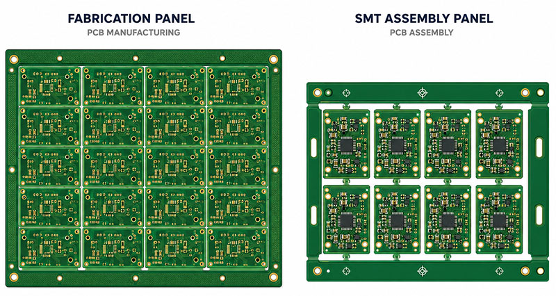
Fabrication Panel vs SMT Assembly Panel

When discussing common PCB panel sizes, it is important to know which panel you mean. PCB fabrication and PCB assembly may use different panel sizes.

Panel TypeUsed InMain Purpose
Fabrication panelPCB manufacturingImprove laminate utilization
SMT assembly panelPCB assemblyFit SMT machines and conveyors
Customer delivery panelFinal delivery or assemblySupport handling and testing

A PCB factory may first produce boards on a large fabrication panel, then cut or score them into smaller customer panels.

For SMT assembly, the panel must fit stencil printing, pick-and-place machines, reflow soldering, AOI, and testing fixtures. This is why SMT panels are often smaller and easier to handle than large fabrication working panels.

This also explains why different manufacturers may recommend different panel sizes for the same PCB design.

Common PCB Panel Sizes

How PCB Board Dimensions Affect Panel Size?

Before choosing a PCB panel size, you need to understand the size and shape of the individual PCB unit. PCB board dimensions directly affect how many units can fit into one panel.

  • Small boards can usually be grouped into larger arrays. This improves SMT efficiency and reduces handling problems. However, very small boards may need extra rails, tabs, or breakaway support.
  • Large boards take up more panel area and reduce the number of units per panel. A large board may also require a stronger panel design to prevent bending during production.
  • Irregular boards are more difficult to panelize than rectangular boards. They may require tab routing, mouse bites, and extra spacing. This can reduce material utilization.
  • High-density boards, edge connectors, tall components, or fragile components may also require more clearance around break lines. In this case, the best panel layout is not always the one with the highest number of boards.

PCB board dimensions affect panel size mainly through:

  • Unit length and width
  • Board shape
  • Component placement
  • Board-to-board spacing
  • Routing or V-cut method
  • Process rail requirement
  • Depanelization safety
  • Usable panel area

A good panel layout should balance board quantity, material usage, assembly stability, and safe separation.

How to Choose the Right PCB Panel Size?

The right PCB panel size should match both PCB fabrication and SMT assembly requirements. A larger panel may increase board count, but it can also increase bending, warpage, and handling risk.

When choosing a PCB panel size, check these factors:

  • PCB board dimensions: Larger boards reduce the number of units per panel.
  • Usable panel area: Tooling holes, coupons, rails, and margins reduce available space.
  • Board shape: Irregular shapes may need tab routing and extra spacing.
  • Panel rails: Rails improve SMT handling but increase final panel size.
  • Depanelization method: V-cut and tab routing require different spacing rules.
  • Component clearance: Edge components need enough distance from break lines.
  • Board thickness: Thin boards may bend more easily in large panels.
  • Copper weight: Heavy copper PCBs may need better panel support.
  • SMT machine limits: The panel must fit production equipment.
  • Shipping and handling: Oversized panels may bend or become damaged.

For small PCBs, grouping many units into one panel can improve production efficiency. For thin, long, heavy, or irregular PCBs, a smaller panel may be safer.

The best PCB panel size is not simply the largest possible panel. It is the size that supports stable manufacturing, good material utilization, smooth assembly, and safe depanelization.

PCB Panel Size Calculation and Panel Utilization

A PCB panel calculator is used to estimate how many PCB units can fit into one panel. It helps engineers compare different panel layouts before production.

To estimate the final panel size, start with the size of one PCB unit and the number of units in the X and Y directions. Then add the required spacing, routing gap, V-cut clearance, process rails, tooling holes, fiducial marks, and edge margin.

For example, if one PCB is 50 Ɨ 30 mm and the panel uses a 4 Ɨ 5 layout, the PCB unit area before adding process space is:

  • X direction: 50 mm Ɨ 4 = 200 mm
  • Y direction: 30 mm Ɨ 5 = 150 mm

The final panel will be larger than 200 Ɨ 150 mm because extra space is still needed for board-to-board spacing, process rails, tooling holes, fiducials, and depanelization clearance. In this case, the actual panel may become about 220 Ɨ 170 mm, depending on the manufacturer’s design rules.

Panel utilization means how efficiently the panel area is used. Higher utilization can reduce material waste, but it should not be the only goal. If the PCB units are placed too tightly, the panel may become difficult to route, score, assemble, inspect, or separate.

A PCB panel calculator is useful for early planning, but the final panel layout should always be reviewed by the PCB manufacturer or assembly supplier before production.

PCB Panel Design Guidelines

PCB panel design guidelines help make sure the panel can be fabricated, assembled, inspected, and separated smoothly.

Choose a Practical Panel Size

  • The panel should fit the manufacturer’s equipment. A panel that is too small may be difficult to handle. A panel that is too large may bend, warp, or exceed machine limits.
  • For many SMT projects, a medium-size panel is more stable than an oversized panel.

Add Process Rails When Needed

  • Process rails help SMT conveyors hold the panel during solder paste printing, pick-and-place, reflow soldering, and inspection.
  • Common rail widths are often around 5 mm to 10 mm, but the final value should follow the assembly supplier’s requirements.

Use Fiducial Marks

  • Fiducial marks help SMT machines align the panel accurately. Panel fiducials are usually placed on the panel rails or panel corners.
  • For fine-pitch components, BGAs, or high-density areas, local fiducials may also be needed.

Include Tooling Holes

  • Tooling holes help with positioning during fabrication, assembly, testing, or fixture use. Their size and location should follow the manufacturer’s process requirements.

Choose V-Cut or Tab Routing Correctly

  • V-cut is suitable for rectangular boards and straight-line separation.
  • Tab routing is better for irregular shapes, curved outlines, or boards with special mechanical edges. Mouse bites are often added to tab-routed panels to make separation easier.

Keep Components Away from Break Lines

  • Components should not be placed too close to V-cut lines, routed edges, tabs, or mouse bites. Tall components, connectors, ceramic parts, and fragile components need more clearance to avoid damage during depanelization.

Control Panel Strength

  • Thin boards, long narrow boards, or panels with too many routed slots may become weak. A weak panel can bend during SMT assembly and cause soldering defects.

Do Not Only Chase Maximum Board Count

  • High material utilization can reduce cost, but over-optimized panels may create assembly or depanelization problems.
  • The goal is not only to fit more boards. The goal is stable production.

What Should Be Included in a PCB Panel Drawing?

A PCB panel drawing shows how individual boards are arranged in the panel. It helps the PCB manufacturer and assembly supplier understand the required panel layout.

A good PCB panel drawing should include:

  • Final panel size
  • Single PCB size
  • Number of PCB units per panel
  • Board orientation
  • Board-to-board spacing
  • Process rail width
  • V-cut lines or routing paths
  • Tab locations
  • Mouse bite details
  • Tooling hole size and position
  • Fiducial mark size and position
  • Component keep-out areas
  • Breakaway direction
  • Dimension units, such as mm or inches
  • Special notes for edge connectors or mechanical parts

For SMT assembly, the panel drawing should match the Gerber files, pick-and-place file, solder paste layer, and BOM. If the panel drawing conflicts with the production files, the manufacturer will need clarification before production.

Before finalizing the panel, ask your manufacturer:

  • What panel sizes do you support?
  • What is the usable panel area?
  • What rail width do you recommend?
  • What are your fiducial and tooling hole requirements?
  • Do you recommend V-cut or tab routing for this board?
  • Can you review the panel drawing before production?

These questions help avoid redesign, production delay, and assembly risk.

FAQs About Common PCB Panel Sizes

What are common PCB panel sizes?

Common PCB panel sizes include 250 Ɨ 250 mm, 250 Ɨ 300 mm, 300 Ɨ 400 mm, 400 Ɨ 500 mm, 457 Ɨ 610 mm, 508 Ɨ 610 mm, and 610 Ɨ 914 mm. The final size depends on the PCB manufacturer, SMT PCB assembly process, and panel design requirements.

What is the most common PCB panel size?

There is no single most common PCB panel size for every project. For SMT assembly, 250 Ɨ 300 mm and 300 Ɨ 400 mm are practical reference sizes. For PCB fabrication, 457 Ɨ 610 mm and 508 Ɨ 610 mm are common working panel sizes.

Are PCB panel sizes standardized?

PCB panel sizes have common reference values, but they are not fixed universal standards. Different factories may use different panel sizes based on equipment, laminate size, routing process, and assembly capability.

What is a PCB panel calculator used for?

A PCB panel calculator is used to estimate how many PCB units can fit into one panel, the approximate final panel size, and the material utilization rate. It is useful for early cost and layout planning.

What is the difference between V-cut and tab routing?

V-cut uses straight scored lines to separate rectangular boards. Tab routing uses routed slots and small tabs to hold PCB units together, making it more suitable for irregular board shapes or special outlines.

What should be included in a PCB panel drawing?

A PCB panel drawing should include final panel size, single board size, board quantity, orientation, spacing, rails, V-cut or routing paths, tabs, mouse bites, tooling holes, fiducial marks, and special assembly notes.

In summary, common PCB panel sizes are useful reference dimensions, but they are not fixed universal standards. The right panel size depends on PCB board dimensions, usable panel area, SMT assembly limits, V-cut or tab routing, tooling holes, fiducials, board thickness, and handling requirements.

For early planning, 250 Ɨ 300 mm, 300 Ɨ 400 mm, 457 Ɨ 610 mm, and 508 Ɨ 610 mm can be used as common references. Before production, the final panel size should always be confirmed with your PCB manufacturer or assembly supplier.

Need support with PCB panel design, full turnkey PCB assembly, panel drawing review, or DFM checking? Send your Gerber files, BOM, panel drawing, and project requirements to EBest Circuit at sales@bestpcbs.com.

You may also like

How to Optimize PCB Panelization for Higher Yield and Lower Cost?
Thursday, May 22nd, 2025

PCB panelization is a critical step in the manufacturing process that directly impacts production efficiency, material waste, and overall costs. Poor panel design can lead to lower yields, increased scrap, and delays in assembly. In this blog, we’ll explore actionable strategies to optimize PCB panelization for higher yield and cost savings.

How to Optimize PCB Panelization for Higher Yield and Lower Cost?

Why Panelization Matters in PCB Manufacturing?

Panelization refers to arranging multiple PCB designs onto a single manufacturing panel (or “array”) for batch processing. Key benefits include:

  • Reduced material waste: Maximizing panel space utilization.
  • Faster assembly: Enabling automated pick-and-place machines to process multiple boards simultaneously.
  • Lower handling costs: Fewer individual boards to manage during fabrication and assembly.

However, suboptimal panelization can lead to:

  • Warpage during soldering.
  • V-score or routing errors.
  • Increased breakage during depaneling.

6 Tips to Optimize PCB Panelization

Base on our 19+years experiences in the PCB manufacturing field, today I would like to share you 6 Strategies to Optimize PCB Panelization

1. Choose the Right Panel Size

  • Align your PCB dimensions with standard panel sizes (e.g., 18″x24″, 21″x24″) to minimize material trimming.
  • Example: If your board is 80mm x 60mm, arrange 4×6 units on a 324mm x 480mm panel to reduce unused space.
6 Tips to Optimize PCB Panelization

2. Optimize Board Arrangement

  • Rotation: Rotate boards to fit more units per panel.
  • Mirroring: Use symmetrical designs to avoid “wasted” gaps.
  • Nesting software: Leverage tools likeĀ CAM350Ā to automate optimal layout generation.

3. Select the Best Depaneling Method

The choice of depaneling (separating individual boards) affects yield and edge quality:

  • V-Score: Low cost and fast, but requires straight edges and may weaken boards.
  • Tab Routing: Ideal for irregular shapes but adds milling time.
  • Laser Cutting: Precision for high-density designs, but higher cost.

Rule of thumb: Use V-score for rectangular boards and routing for complex shapes.

4. Add Breakaway Tabs and Mouse Bites

  • Breakaway tabs: Small connectors between boards to prevent movement during assembly.
  • Mouse bites: Perforated holes for easy manual separation.
  • Spacing: Maintain 1.5–2mm between boards to avoid solder mask bridging.
How to Optimize PCB Panelization for Higher Yield and Lower Cost?

5. Incorporate Fiducials and Tooling Holes

  • AddĀ global fiducialsĀ to the panel for accurate alignment during SMT assembly.
  • IncludeĀ tooling holesĀ (3.2mm diameter) to secure the panel during drilling and routing.

6. Balance Quantity vs. Risk

  • Overcrowding panelsĀ increases the risk of cross-board defects.
  • Underutilizing panelsĀ raises material costs.
  • Recommended: Aim for 4–20 boards per panel, depending on size and complexity.

Case Study: Cost Savings Through Smart Panelization

A consumer electronics manufacturer redesigned their 50mm x 50mm IoT module panel:

  • Initial design: 8 boards/panel with 15% wasted space.
  • Optimized design: 12 boards/panel using rotated layouts and shared tooling holes.
  • Results:
    • 15% reduction in material costs.
    • 10% faster SMT assembly.
    • Fewer depaneling errors due to improved tab routing.

Common Panelization Mistakes to Avoid

  1. Ignoring manufacturer capabilities: Always consult your PCB fab’s panel size and tolerances.
  2. Overcomplicating shapes: Complex panels increase milling time and scrap rates.
  3. Skipping test coupons: Include test patterns for impedance control and quality checks.

Conclusion

Optimizing PCB panelization requires a balance of geometric efficiency, process knowledge, and collaboration with manufacturers. By implementing these strategies, you can reduce waste, improve yields, and lower production costs without compromising quality.

Pro Tip: Use panelization-specific design rules in tools likeĀ AltiumĀ orĀ KiCadĀ to automate compliance checks.

Also, if you want to know more about how to optimize PCB Panelization for Higher Yield and Lower Cost, please feel free to inquiry from us.

You may also like