PCB manufacturing PCB manufacturing
Home > Blog

RF PCB

High Frequency PCB Manufacturer Selection Guide
Wednesday, July 15th, 2026
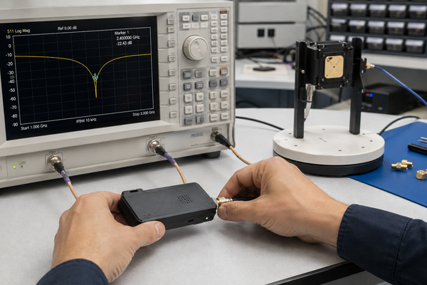
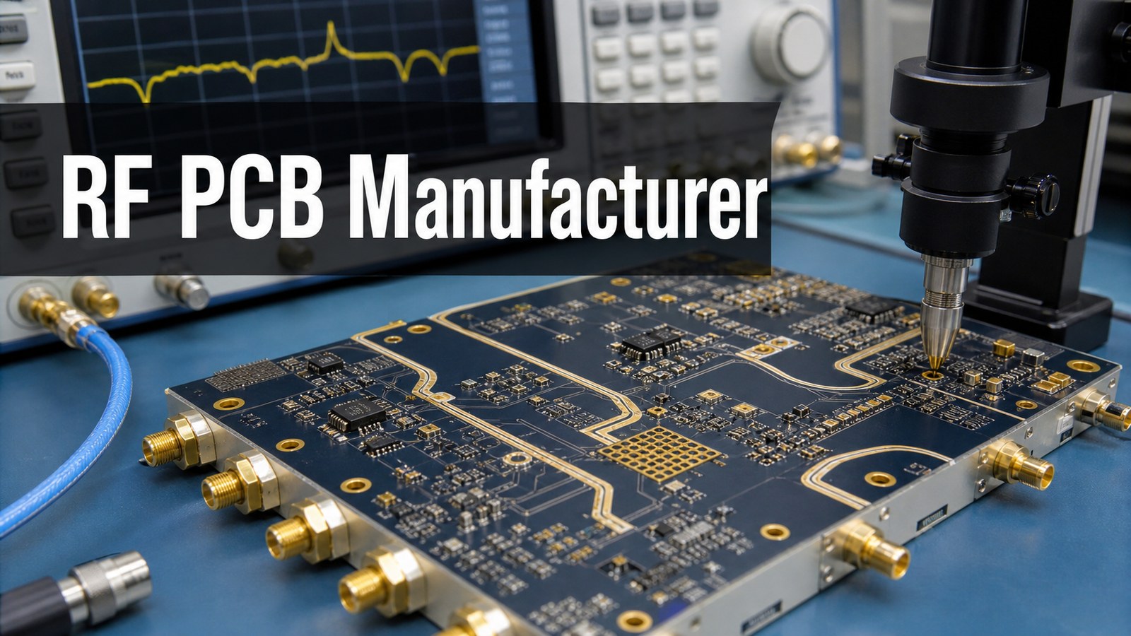
High frequency PCB manufacturer RF board testing and inspection

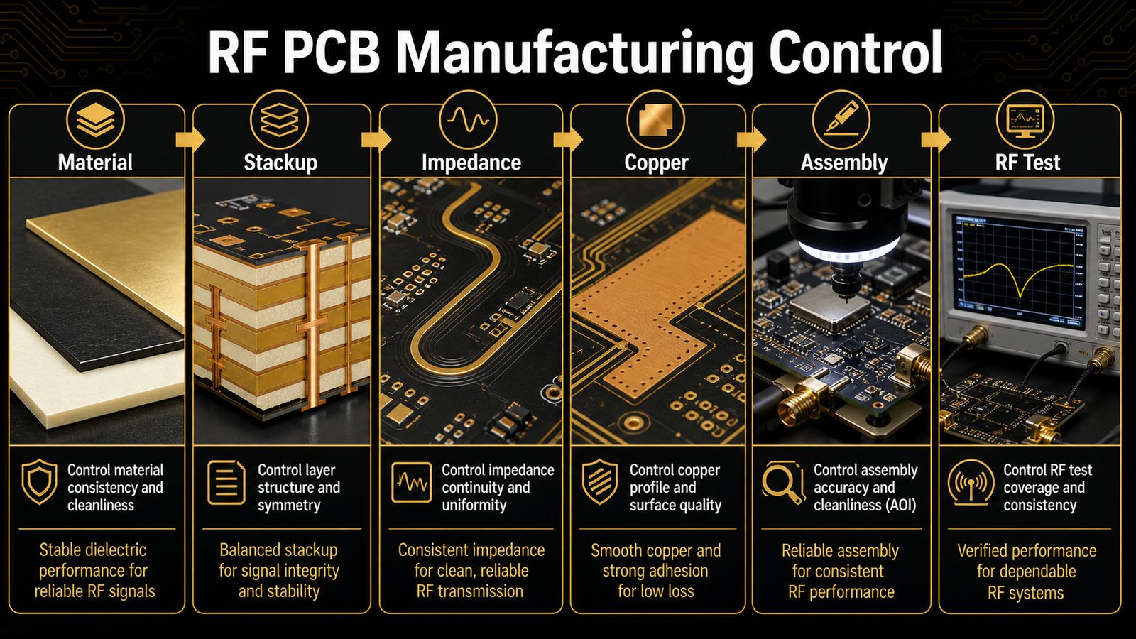
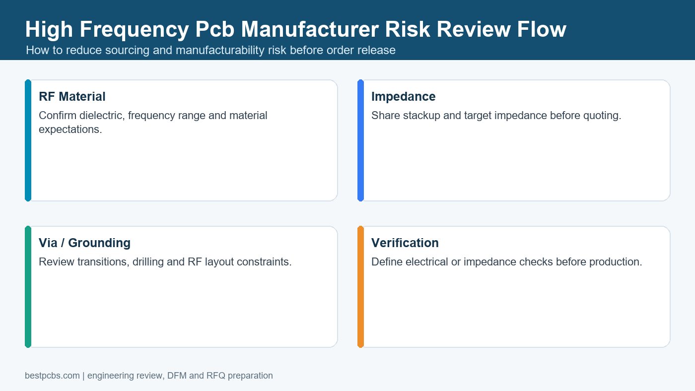
A high frequency PCB manufacturer should understand RF materials, controlled impedance, low-loss stackups, copper treatment, dimensional control, testing expectations and DFM review before quoting the board. The buying risk is that a supplier may say it can build high frequency PCBs without clarifying the material, frequency, impedance or verification method.

This guide explains how to evaluate a high frequency PCB supplier, what the Google top results show, what technical details affect cost and quality, and what to include in an RFQ.

High Frequency PCB Manufacturer at a Glance

The right high frequency PCB supplier should quote the board as an RF or microwave engineering build, not as a generic FR-4 PCB with a different keyword. The buyer should provide material expectations, stackup, impedance targets, frequency range, copper requirements and test needs early.

Area What to confirm Why it matters
Material RF laminate, high-speed laminate or hybrid stackup Loss, stability and manufacturability depend on material choice.
Stackup Reference planes, dielectric thickness and impedance targets High frequency behavior depends on geometry, not only copper routing.
Manufacturing Drilling, registration, copper finish, etching and dimensional control Small deviations can change RF performance.
Testing Electrical, impedance, coupon, functional or RF test scope The buyer must know what the supplier can verify before shipment.

What Google Top Results Show

The Google US results are strongly commercial: high frequency PCB manufacturer pages, RF and microwave PCB service pages, material-focused supplier pages, top manufacturer lists, technical guides and a few video or forum results. Top results include RF/MW manufacturing pages, high frequency PCB supplier pages and pages referencing materials such as Rogers, Isola, Taconic and Arlon.

The ranking opportunity is to combine buyer-level supplier evaluation with engineering details that help the searcher avoid a weak quote.

What Counts as a High Frequency PCB?

A high frequency PCB is a circuit board designed for RF, microwave or high-speed signal behavior where material loss, impedance, dielectric stability and geometry control matter. There is no single buying rule that fits every board, so the project files and intended signal behavior must be reviewed.

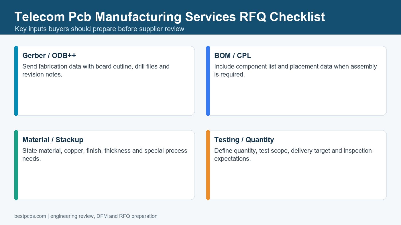
For a closely related topic, compare this guide with the RF PCB manufacturer RFQ guide.

Materials Used in High Frequency PCB Manufacturing

Material selection is one of the first decisions because high frequency behavior is directly affected by dielectric properties, loss and thickness control. Buyers may specify an RF laminate, a high-speed material, a hybrid stackup or a supplier-recommended material after review.

Do not publish a material claim into the order unless it is confirmed in the RFQ and latest process capability data. If the material is a target rather than a requirement, say so and ask the supplier to confirm availability and manufacturability.

Impedance, Stackup and RF Layout Notes

Controlled impedance and stackup requirements should be written in the fabrication package, not inferred from the copper artwork alone. High frequency layouts often depend on trace width, dielectric thickness, copper roughness, return paths, via transitions and connector launches.

  • State impedance values and tolerance requirements.
  • Provide stackup targets and reference plane expectations.
  • Identify RF traces, antennas, filters, feed lines and connector areas.
  • Clarify whether impedance coupons or RF tests are required.
  • Separate ordinary control circuitry from RF-sensitive sections.

DFM Review for High Frequency PCBs

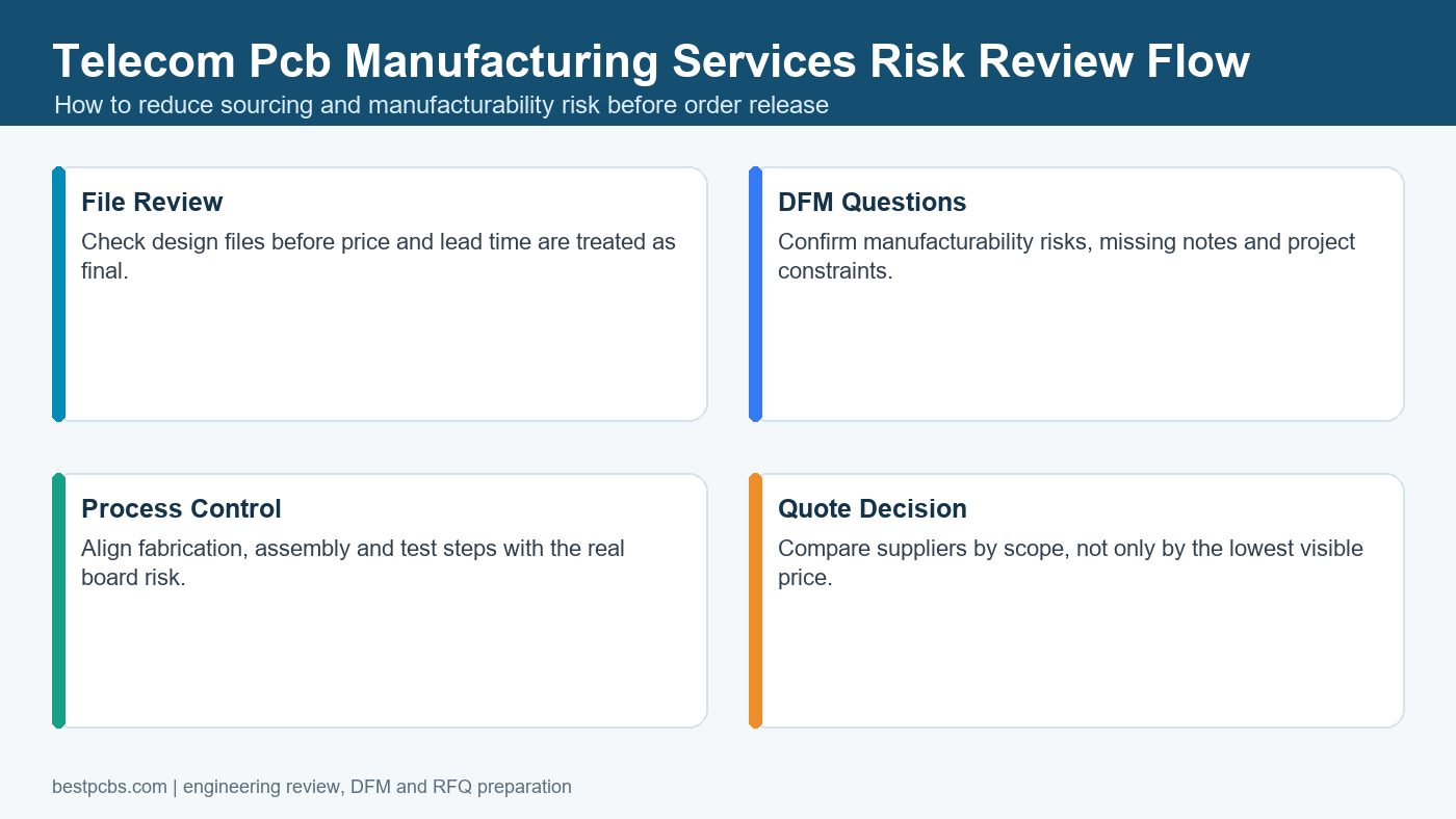
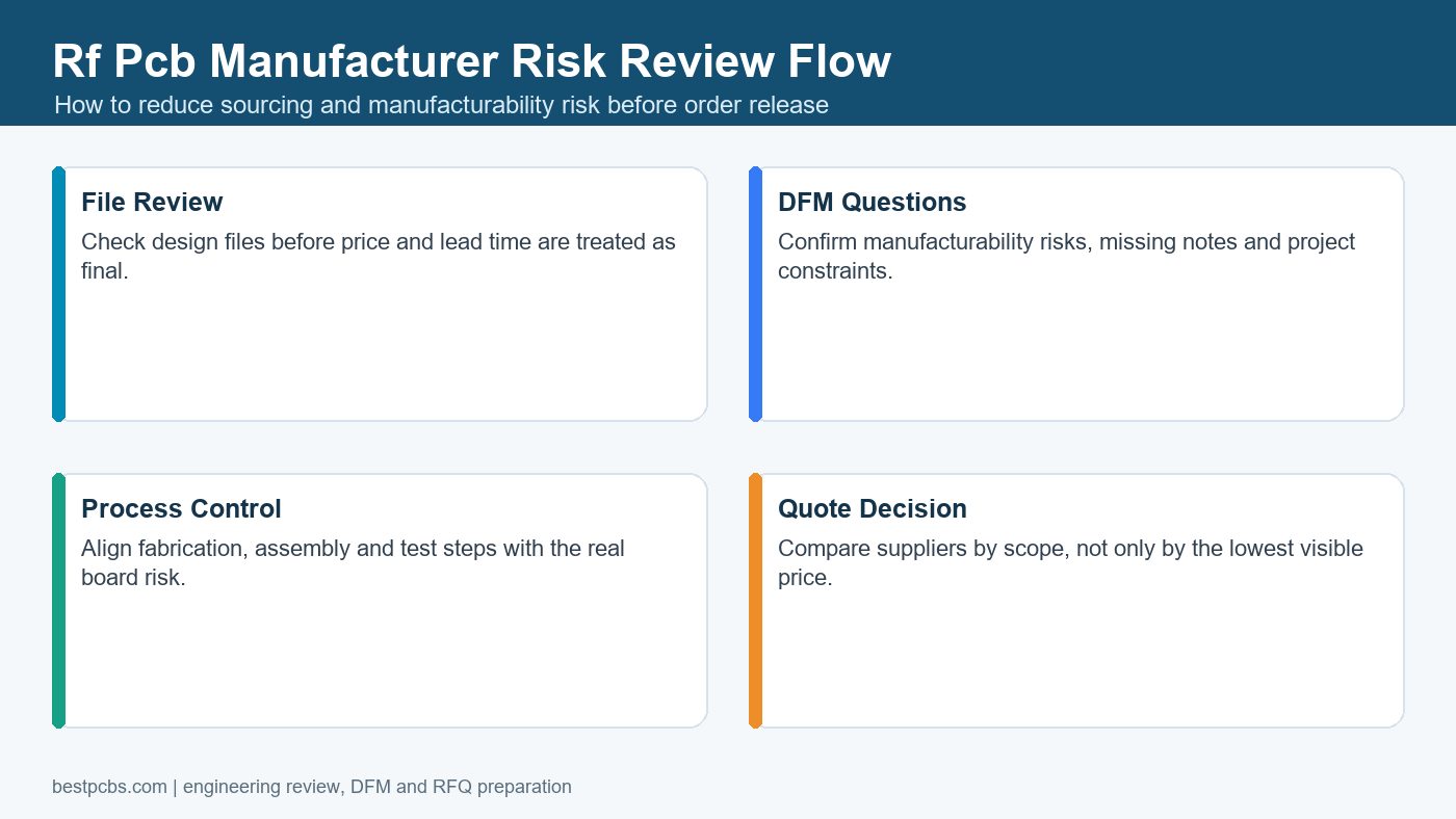
DFM review should catch manufacturing changes that could alter RF performance before the order is released. The review should cover material, drill sizes, annular rings, copper features, solder mask openings, panelization, controlled impedance notes and special process instructions.

If the board also needs ordinary design checks, use the PCB design and manufacturing DFM guide alongside the RF-specific review.

High Frequency PCB Assembly Considerations

Assembly planning matters because RF connectors, shields, modules, fine-pitch components and test access can affect both performance and inspection. A bare board supplier and an assembly supplier should not make separate assumptions about RF areas.

For assembled boards, prepare BOM, CPL, assembly drawing, polarity notes, approved substitutes, RF connector requirements and test procedure. The PCBA service is a useful path when fabrication and assembly need one coordinated review.

Testing and Verification

Testing should be defined before quote approval because not every supplier can verify RF behavior beyond bare-board electrical and impedance checks. If functional or RF performance testing is needed, the buyer may need to provide fixtures, firmware, calibration requirements and pass/fail limits.

Check What it verifies Buyer responsibility
Electrical test Open and short conditions Provide netlist and test scope.
Impedance test Controlled impedance behavior on coupons or traces Provide target values and tolerances.
Assembly inspection Placement, soldering, polarity and connector quality Provide BOM, CPL and drawings.
RF or functional test Application-level behavior Provide fixtures, firmware and acceptance criteria.

How to Compare High Frequency PCB Suppliers

Compare high frequency PCB suppliers by their questions and assumptions, not only by unit price. A credible supplier should ask about material, stackup, impedance, test method, frequency-sensitive sections and assembly requirements.

  • Can the supplier discuss RF materials and hybrid stackups without vague claims?
  • Can they review controlled impedance requirements before production?
  • Can they state what testing is included and what requires buyer fixtures?
  • Can they coordinate fabrication and assembly when connectors or shields matter?
  • Do they document quote assumptions instead of hiding uncertainty?

What Determines High Frequency PCB Cost?

High frequency PCB cost depends on RF material, layer count, stackup complexity, impedance control, board size, drilling, finish, testing, quantity and assembly needs. Supplier quotes can vary widely because material and verification assumptions are not always the same.

For broader cost planning, compare the project with the custom PCB cost guide, then ask every supplier to quote the same stackup and test scope.

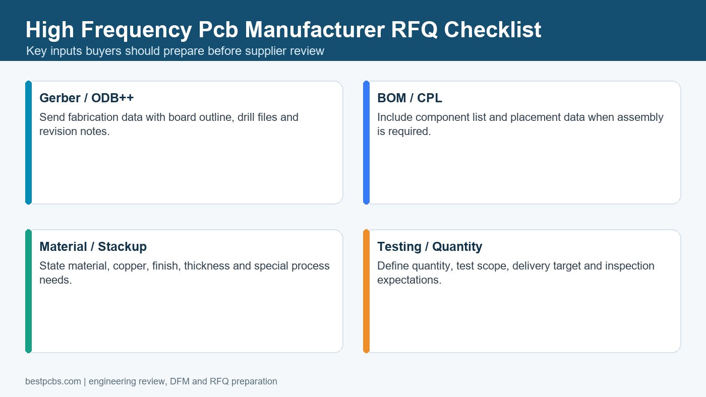
RFQ Checklist for a High Frequency PCB Manufacturer

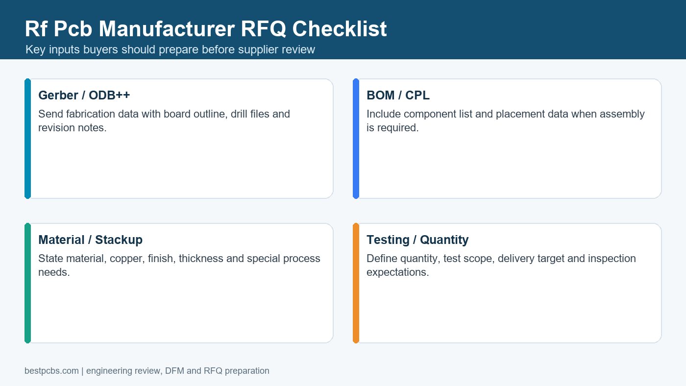
A strong RFQ should give the manufacturer enough information to quote RF performance risk, not only board size and layer count. Missing material or impedance information can make the first quote unreliable.

  • Gerber or ODB++ files, drill files and fabrication drawing.
  • Material target, stackup, copper, board thickness and surface finish.
  • Controlled impedance values, tolerance and reference plane notes.
  • RF areas, connector launches, shields and test requirements.
  • BOM, CPL, assembly drawing and polarity notes if PCBA is needed.
  • Quantity, target lead time, packaging and delivery destination.

Frequently Asked Questions About High Frequency PCB Manufacturers

Is a high frequency PCB the same as an RF PCB?

The terms often overlap. RF PCB usually refers to radio-frequency behavior, while high frequency PCB can include RF, microwave or high-speed signal applications depending on the project.

Can standard FR-4 be used for high frequency PCBs?

Sometimes, for less demanding sections or lower-risk designs. Higher frequency, lower loss or tighter impedance requirements may need a different material. The material choice should be confirmed by project review.

What should I send to quote a high frequency PCB?

Send Gerber or ODB++, drill files, stackup, material target, impedance requirements, quantity and delivery target. For assembly, also send BOM, CPL and drawings.

What is the biggest sourcing risk?

The biggest risk is accepting a quote that does not define material, impedance, test scope or assembly assumptions. That can create performance or schedule problems after production begins.

Final RFQ Recommendation

Before choosing a high frequency PCB manufacturer, document the RF-sensitive parts of the design and the verification method you expect. The supplier can quote more accurately when material, stackup, impedance and test scope are visible.

For a high frequency PCB quote, send your Gerber or ODB++ files, drill data, stackup, material targets, impedance notes, BOM, CPL, assembly drawing, quantity, surface finish, testing requirements and target lead time to sales@bestpcbs.com. The Best Technology / bestpcbs team can review the files and confirm what needs project-specific checking before production.

You may also like

Telecom PCB Manufacturing Services Guide
Wednesday, July 15th, 2026
Telecom PCB manufacturing services for RF and communication boards

Telecom PCB manufacturing services cover the fabrication, assembly, inspection and testing decisions needed for communication equipment boards, especially when RF behavior, signal integrity, material choice, shielding, thermal load or production repeatability matters. The right supplier should help the buyer review the board as an engineered communication product, not only quote a generic PCB.

This guide explains how to compare telecom PCB suppliers, what the current Google results show, which technical requirements should be clarified, and what files to send for a useful RFQ.

Telecom PCB Manufacturing Services at a Glance

A telecom PCB service should connect bare board fabrication, DFM review, assembly planning, RF-related checks, testing expectations and quote assumptions. The exact requirement depends on whether the board is a base station module, router board, antenna interface, IoT gateway, fiber equipment board, power board or control PCB.

Area What to confirm Why it matters
Electrical behavior Controlled impedance, RF paths, return paths and signal integrity needs Telecom boards can fail even when the bare board passes simple continuity tests.
Materials FR-4, high-frequency material, hybrid stackup or project-specific laminate Material choice affects loss, stability, cost and manufacturability.
Assembly BOM, CPL, shielding, connectors, polarity and inspection access RF modules, connectors and shielding parts can drive assembly risk.
Testing Electrical test, AOI, X-ray if needed, functional or RF test responsibility The buyer must know what the supplier can verify before shipment.

What Google Top Results Show

The Google US top results combine telecom-specific PCB assembly pages, general PCB manufacturers, USA supplier comparisons, EMS pages, directories and local assembly providers. Examples in the collected results include EMSG telecom assembly content, AdvancedPCB, Sierra Assembly, Blind Buried Circuits, Technotronix, FS Circuits, Foxtronics EMS, PCB Directory and Green Circuits.

This SERP suggests a mixed intent: some searchers want a telecom-capable manufacturer, while others compare local EMS providers or general PCB suppliers. A ranking-focused Blog should therefore explain supplier selection and telecom requirements before asking for an RFQ.

What Makes Telecom PCBs Different?

Telecom PCBs are different when the board carries RF signals, high-speed data, stable clocking, dense connectors, shielding, thermal load or long production life requirements. Not every telecom board is high-frequency, but every telecom project should identify which sections are electrically sensitive.

A simple control board inside communication equipment may use standard PCB rules. A board with antennas, RF front ends, filters, high-speed interfaces or impedance-controlled lines needs closer review. For RF-specific buying questions, the RF PCB manufacturer RFQ guide is a useful supporting reference.

Materials and Stackup for Telecom PCB Projects

Material and stackup should be selected after the signal behavior, thermal load, layer count, impedance needs and assembly process are understood. Standard FR-4 may be appropriate for many control and power areas, while RF or high-speed sections may need a different laminate or hybrid construction.

Buyers should send the target stackup, copper weight, impedance requirements, operating frequency if relevant, board thickness, surface finish and any thermal notes. Exact material capability and special process limits must be confirmed from the latest project data before order release.

RF, Impedance and Signal Integrity Checks

RF and impedance requirements should be stated in the fabrication notes instead of left for the supplier to infer from the Gerber files. Missing impedance targets, reference planes, material assumptions or test methods can create quote changes and production uncertainty.

  • State controlled impedance values and tolerance requirements if applicable.
  • Provide stackup targets and dielectric material expectations.
  • Identify RF paths, antenna areas, ground references and shielding zones.
  • Clarify whether the supplier is responsible for impedance coupon testing.
  • Separate ordinary digital/control areas from RF-sensitive sections.

Telecom PCB Assembly and Component Sourcing

Telecom PCB assembly should be planned with connectors, shielding, RF modules, fine-pitch components, thermal parts and component availability in mind. A bare PCB quote does not answer whether the final board can be assembled cleanly.

If the project needs mounted components, prepare BOM, CPL, assembly drawing, polarity notes, approved substitutes and any testing instructions. The PCBA service is the right internal path when fabrication, assembly and sourcing need to be reviewed together.

DFM Review Before Telecom PCB Production

DFM review should catch manufacturability risks before the telecom board is quoted as a production job. This includes drill-to-copper clearance, solder mask openings, fine-pitch pads, via design, copper balance, controlled impedance notes, panelization and assembly access.

For production-oriented layouts, compare the board against a PCB design and manufacturing DFM guide before release. If RF or high-speed rules are unclear, label them as targets and ask the supplier to confirm what can be manufactured and tested.

Testing and Inspection for Telecom PCBs

Testing should be defined before the order because telecom boards may need more than a standard bare-board electrical test. A supplier can verify open/short conditions, visual quality and assembly defects, but RF performance or functional behavior may need buyer-supplied fixtures and acceptance rules.

Test or inspection What it checks Buyer input needed
Electrical test Bare board opens and shorts Gerber, netlist and test expectations
AOI / visual inspection Soldering, placement and visible defects Assembly files, polarity and acceptance criteria
Impedance test Controlled impedance coupon or trace behavior Target values, tolerance and stackup
Functional or RF test Board-level communication or signal performance Fixture, firmware, procedure and pass/fail limits

How to Compare Telecom PCB Suppliers

Compare suppliers by whether they can discuss the actual telecom risk in the board, not only by whether they list PCB manufacturing services. A good supplier should ask about stackup, impedance, materials, assembly files, test method and delivery requirements.

  • Can the supplier review RF or impedance notes before quote approval?
  • Can they support both PCB fabrication and assembly if required?
  • Do they identify special materials or processes that need confirmation?
  • Do they explain what testing is included and what requires buyer fixtures?
  • Can they quote prototype, low-volume and repeat production needs separately?

What Determines Telecom PCB Manufacturing Cost?

Telecom PCB cost is shaped by material, layer count, impedance control, board size, copper, finish, connector complexity, assembly method, testing, quantity and delivery expectations. A lower quote may be valid for a simple control board but incomplete for an RF or high-speed communication board.

For cost planning, compare telecom requirements with the custom PCB cost guide, then ask suppliers to quote the same stackup, finish, testing and assembly scope.

RFQ Checklist for Telecom PCB Manufacturing Services

A telecom PCB RFQ should include enough detail for the supplier to identify fabrication, assembly and testing risk before committing to price and lead time. Short requests such as “telecom PCB quote” usually lead to follow-up questions.

  • Gerber or ODB++ files, drill data and fabrication drawing.
  • Layer count, stackup, material, copper, thickness and surface finish.
  • Controlled impedance values, RF notes or high-speed constraints if applicable.
  • BOM, CPL, assembly drawing, polarity notes and substitute rules for PCBA.
  • Quantity, prototype or production stage, target lead time and delivery destination.
  • Electrical test, impedance test, functional test or RF test expectations.

Frequently Asked Questions About Telecom PCB Manufacturing

Are all telecom PCBs high-frequency PCBs?

No. Some telecom boards are power, control or interface boards using standard materials. Others include RF or high-speed sections that need special stackup, material and impedance review.

Can one supplier handle telecom PCB fabrication and assembly?

Yes, if the supplier supports both PCB manufacturing and PCBA. A combined review can reduce handoff mistakes between Gerber files, BOM, CPL, assembly notes and testing requirements.

What should I send for a telecom PCB quote?

Send Gerber or ODB++, drill files, stackup, material, impedance notes, finish, quantity and delivery target. For assembly, also send BOM, CPL, drawings, polarity notes and test requirements.

How do I avoid quality problems in telecom PCB sourcing?

Define the sensitive circuit areas, state material and test assumptions, request DFM review, and confirm what the supplier can actually verify before shipment.

Final RFQ Recommendation

Before choosing telecom PCB manufacturing services, identify whether the board is mainly standard fabrication, RF/high-frequency, high-speed, assembly-heavy or test-heavy. The supplier can quote more accurately when the technical risk is visible.

For a telecom PCB fabrication or assembly quote, send your Gerber or ODB++ files, drill data, stackup, impedance notes, BOM, CPL, assembly drawing, quantity, material expectations, surface finish, testing requirements and target lead time to sales@bestpcbs.com. The Best Technology / bestpcbs team can review the project files and confirm what needs project-specific checking before production.

You may also like

RF PCB Manufacturer Selection and RFQ Guide
Wednesday, July 15th, 2026
RF PCB manufacturer inspecting high frequency circuit board with RF connectors

An RF PCB manufacturer builds circuit boards for radio-frequency and microwave signals where laminate choice, controlled impedance, copper geometry, surface finish and test planning affect signal loss and repeatability. For buyers, the practical question is whether the supplier can review material, stackup, transmission-line geometry, connector launch, impedance targets and RFQ files before fabrication.

This guide focuses on commercial RF, wireless, telecom, sensor and high-frequency electronics projects. Specific capability references come from Best Technology / bestpcbs process records where the data is available, and project-specific compliance requirements should be confirmed before quotation.

RF PCB Manufacturer at a Glance

A reliable RF PCB manufacturer should treat the board as part of the signal path, not only as a carrier for components. Small changes in laminate, dielectric thickness, copper roughness, trace width, solder mask and connector launch can change RF performance.

RF decision area What to confirm Why it matters
Material Rogers, Taconic, PTFE, high-Tg FR4 or hybrid stackup Controls dielectric constant, loss and availability.
Impedance Target value, tolerance, trace type and reference plane Reduces reflection and mismatch.
Stackup Layer count, dielectric thickness, copper weight and mixed materials Controls repeatability and manufacturability.
RF details Connector launch, via fence, grounding, transition and keepout rules Prevents avoidable RF loss or instability.

What the Current Google Results Show

The current Google results for this keyword are dominated by RF and microwave PCB manufacturer pages, supplier directories, high-frequency material pages and Top manufacturer comparisons. That means the searcher is usually trying to shortlist suppliers or prepare an RF quote, not read a generic PCB definition.

The top pages win because they mention RF/microwave materials, controlled impedance, quote intent and supplier capability early. A strong bestpcbs blog post can compete by giving a clearer RFQ checklist, material-risk explanation and practical comparison framework.

RF PCB Capabilities Buyers Should Verify

Before selecting an RF PCB manufacturer, verify material availability, line/space capability, surface finish, board thickness range, impedance needs and test expectations. RF capability depends on the exact frequency range, laminate and layout, so a generic claim is not enough.

Capability item Verified bestpcbs reference RFQ note
High-frequency materials Rogers 4003 / 4350 / 5880, Taconic laminates, PTFE, Nelco and other special materials are listed in the capability record. Confirm availability and substitutions before quote release.
Layer count FR4 normal range 1-10 layers, special range 10-32 layers in the referenced PCB capability sheet. Hybrid RF stackups require separate confirmation.
Fine lines 1/2 oz inner layer 4/4 mil normal and 3/3 mil special; 1/1 oz outer layer 4/4 mil normal and 3/3 mil special. Check line width against impedance, copper and finished plating.
Surface finish OSP, HASL, ENIG, immersion silver, immersion tin, ENEPIG and hard-gold-related options are listed with conditions. Choose finish based on assembly, RF pads and connector needs.

RF Materials and Laminate Selection

RF material selection should be driven by dielectric constant, loss tangent, thickness control, copper surface, frequency range, availability and cost. Using a familiar laminate name without checking stackup and supplier availability can create quote delays.

Bestpcbs records list high-frequency material options such as Rogers 4003 / 4350 / 5880, Taconic laminates, PTFE and related high-performance materials. The RF Board manufacturer page and RF PCB product page are useful internal references for the service scope.

Controlled Impedance and Transmission Lines

Controlled impedance should be specified before fabrication because RF traces depend on laminate thickness, copper weight, solder mask, trace geometry and reference plane continuity. The manufacturer should know whether the design uses microstrip, stripline, coplanar waveguide or another controlled structure.

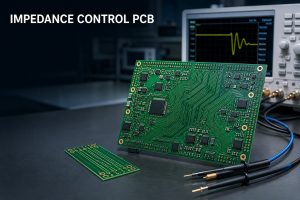
Send target impedance, tolerance, frequency range, layer stackup and whether test coupons are required. For mixed digital and RF boards, also identify high-speed nets, RF nets and sensitive return paths. The impedance control PCB page is a relevant reference.

Connector Launch, Grounding and Via Fencing

Connector launch, grounding and via fencing often determine whether an RF PCB performs well after assembly. A board can use the correct laminate and still perform poorly if transitions, pads or ground stitching are not reviewed.

  • Provide connector part numbers and recommended footprints.
  • Mark RF keepout areas and critical transmission lines.
  • Confirm via fence spacing and grounding expectations.
  • Review transitions between connectors, antennas, filters, amplifiers and test points.
  • State whether RF testing or only manufacturing inspection is required.

Hybrid RF Stackups

Hybrid RF stackups combine high-frequency laminates with FR4 or other materials, so they need a more careful manufacturing review than standard FR4 boards. Material expansion, lamination behavior and thickness control can affect repeatability.

For hybrid builds, send a controlled stackup and identify which layers carry RF signals. If the design combines RF, digital control, power and PCBA in one board, include assembly constraints as part of the RFQ. Related internal reading includes the HDI PCB manufacturer RFQ guide when the design also uses dense routing or microvias.

RF PCB Cost Drivers

RF PCB cost is driven by laminate choice, stackup complexity, impedance control, low-loss material procurement, connector requirements, surface finish, testing and panel utilization. A lower quote may simply exclude material or test assumptions.

Cost driver Why it changes cost How to control it
Special laminate High-frequency materials may have MOQ or longer procurement time. Approve alternates early when possible.
Impedance control Requires stackup calculation and sometimes coupons. Provide target values and tolerance up front.
Connector launch May need footprint review or assembly care. Send connector datasheets and drawings.
Testing RF validation is different from basic electrical test. Define what the supplier must inspect or test.

Prototype and Production RF PCB Orders

Prototype RF PCB orders should prove material, stackup and connector performance before scaling to production. Production orders need stronger material control, repeatable stackups and clear acceptance criteria.

For prototypes, focus on engineering feedback, impedance targets and connector launch checks. For production, define laminate alternates, revision control, inspection records, packaging and whether assembly is included. If PCBA is needed, connect the RF board quote with the PCBA and PCB assembly service.

How to Compare RF PCB Manufacturers

Compare RF PCB manufacturers by their material knowledge, impedance review process, RF layout questions and quote assumptions. A supplier that asks the right RF questions early is more useful than one that only returns the fastest price.

  • Do they ask for frequency range, material and stackup?
  • Can they support controlled impedance and RF coupons if required?
  • Do they separate normal capability from special procurement cases?
  • Do they review connector launches and sensitive transitions?
  • Do they avoid unsupported promises about RF performance without test criteria?

RFQ File Checklist for RF PCB Projects

A complete RF PCB RFQ should include fabrication files, stackup, material, impedance targets, connector data, quantity, surface finish and test requirements. Without these inputs, the quote may not reflect the real RF design.

RFQ item Why it matters
Gerber or ODB++ Defines copper, solder mask, drill, outline and manufacturing data.
Stackup Defines dielectric thickness, laminate, copper and reference planes.
Impedance table Lists RF nets, target values, tolerance and trace type.
Connector datasheets Helps review launch geometry and assembly fit.
BOM, CPL and drawings Required if the project includes assembly or turnkey PCBA.
Test requirements Clarifies whether the supplier performs E-test, impedance, inspection or RF-related checks.

Internal Resources for RF PCB Buyers

RF PCB buyers should connect RF material pages, impedance resources and manufacturing checklists before ordering. Useful internal references include the multilayer PCB manufacturing checklist, the PCB fabrication manufacturer guide, and the PCB assembly manufacturer RFQ checklist when components are part of the project.

Common RF PCB Sourcing Mistakes

Common RF PCB sourcing mistakes include quoting without stackup, changing laminates without impedance review, ignoring connector launch details, and treating all high-frequency suppliers as interchangeable. These mistakes can create performance problems after the board is already assembled.

  • Do not approve laminate substitutions without checking impedance and loss needs.
  • Do not leave connector launch and grounding details out of the RFQ.
  • Do not compare quotes unless material, surface finish and testing assumptions match.
  • Do not assume a basic electrical test proves RF performance.
  • Do not use regulated project assumptions unless the supplier has confirmed the required scope and credentials.

Frequently Asked Questions About RF PCB Manufacturers

What does an RF PCB manufacturer do?

An RF PCB manufacturer fabricates circuit boards for radio-frequency and microwave signals, with attention to laminate choice, impedance, trace geometry, grounding and RF-related assembly constraints.

What materials are used for RF PCBs?

RF PCBs may use high-frequency laminates such as Rogers, Taconic, PTFE-based materials, high-Tg FR4 or hybrid material stackups, depending on frequency, loss target and cost.

Is controlled impedance required for RF PCBs?

Usually yes for defined RF transmission lines. The RFQ should include target impedance, tolerance, stackup and trace type so the manufacturer can review feasibility.

Can RF PCBs also include assembly?

Yes, if the supplier supports PCBA. Assembly planning should include RF connectors, shield parts, sensitive components, test access and handling requirements.

Final RFQ Recommendation

Choose an RF PCB manufacturer that reviews material, stackup, impedance, connector launch, grounding and test expectations before quoting. A precise RFQ is the best way to avoid late material changes and signal-integrity surprises.

For an RF PCB quotation, send your Gerber or ODB++ files, stackup, laminate preference, impedance table, connector datasheets, quantity, surface finish, BOM, CPL, assembly drawings if needed, test requirements and target lead time to sales@bestpcbs.com. The Best Technology / bestpcbs team can review the package and identify which RF manufacturing assumptions need confirmation before prototype, pilot or production release.

You may also like

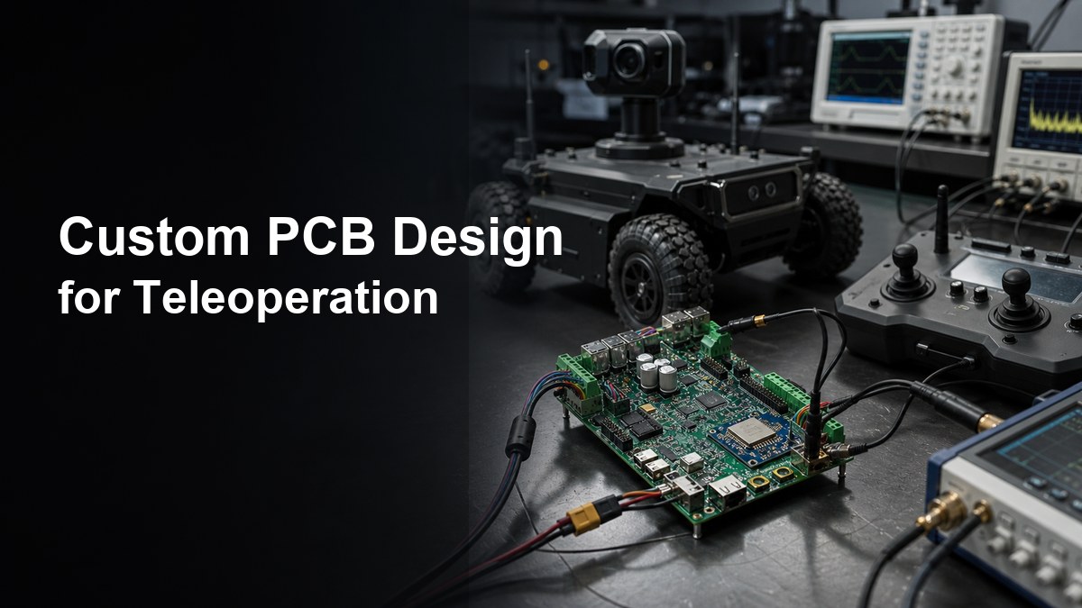
Custom PCB Design for Teleoperation: Latency, Power and RF Checks
Monday, July 13th, 2026
Custom PCB design for teleoperation robot controller with remote control and lab test equipment

Custom PCB design for teleoperation should protect the remote-control link, motor-control power path, sensor feedback, test access and enclosure interface before the first prototype is ordered. A teleoperation PCB is not just a robot controller board. It carries the electronics that help an operator send commands, receive feedback and keep the machine predictable when wireless quality, vibration, load current or cable routing changes.

This guide is written for engineers and buyers preparing a custom PCB or PCBA for teleoperated robots, remote inspection equipment, mobile platforms, industrial manipulators, UAV ground systems, field-service devices or hazardous-area remote tools. It focuses on manufacturable PCB checks and RFQ readiness, not on robot-control algorithms.

What does custom PCB design for teleoperation need to control?

A teleoperation PCB needs to keep command input, feedback data, power conversion, motor drivers, sensors and safety-related I/O electrically separated enough to avoid unstable behavior. The design may include a microcontroller or processor, RF or wired communication module, camera or sensor inputs, encoder lines, motor-driver interfaces, battery or DC input, protection circuits and connectors to the robot body.

The board should be reviewed as a system. A clean schematic can still fail in the field if motor-current return paths disturb the receiver, if a camera interface sits beside a noisy regulator, or if a connector harness pulls against a weak solder joint. When wireless range, antenna routing or controlled impedance matters, compare the design against an RF PCB capability early instead of treating the radio section as a normal digital trace group.

Teleoperation PCB area Design check Why it matters
Communication link Antenna clearance, controlled routing, shielding, connector loss and RF module placement Weak links create command delay, dropouts or unstable feedback
Power input Battery/DC range, transient protection, regulator heat and local decoupling Remote machines often see load surges and cable voltage drop
Motor and actuator paths High-current loops, driver heat, return path and separation from sensors Motor noise can reset logic or corrupt feedback signals
Sensor feedback Encoder, camera, IMU, limit switch and telemetry routing The operator needs reliable state information, not only command output
Production test Programming access, test pads, fixture clearance and functional-test limits A prototype that cannot be tested repeatably is not ready for volume

How should latency and link reliability affect PCB layout?

PCB layout cannot remove all network delay, but it can reduce board-level causes of packet loss, noise coupling and unreliable command response. Teleoperation systems are sensitive to latency, jitter and communication dropouts, so the board should not add avoidable RF, grounding or power noise problems on top of the software and network layer.

Keep the antenna or RF module away from motor drivers, switching regulators, displays, dense cable bundles and metal enclosure walls unless the RF design intentionally accounts for them. Follow the module vendor’s keep-out and ground rules. If the design uses external antennas, review connector type, cable routing, mounting torque and enclosure feedthrough. If it uses wired control, check differential-pair routing, shielding, ESD protection and connector strain relief.

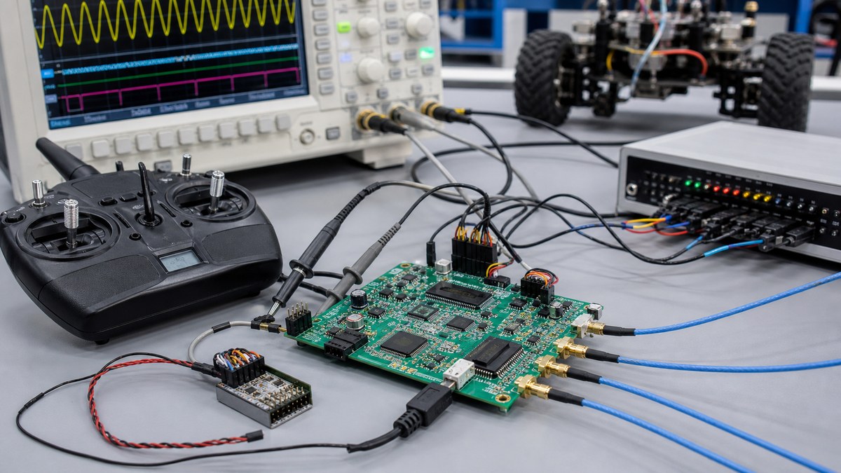
Teleoperation PCB signal validation with oscilloscope, RF cables and remote-control hardware
Teleoperation PCBs should be validated around command signals, feedback data and RF or wired communication paths.

Do not bury the communication decision inside a generic PCB order. If the board includes RF, Ethernet, CAN, RS-485, USB, camera links or high-speed sensor data, the stackup, reference planes and connector placement should be part of the RFQ review. Related control-network design checks are also covered in the custom PCB design for industrial networks guide.

What power architecture should a remote robot controller use?

The power architecture should separate noisy actuator energy from logic, RF, sensors and safety I/O while still sharing a controlled grounding strategy. Teleoperated equipment often combines battery packs, DC input, motor drivers, servos, radios, cameras, lamps, heaters or brakes. Those loads should not all be treated as a single quiet supply problem.

Start by listing each rail, load current, startup sequence, allowable voltage range and heat source. Use local decoupling for processors, RF modules and sensors. Keep high-current switching loops short. Give motor-driver current a planned return path instead of letting it travel under the communication and sensor sections. If the design has high-current power electronics, heavier copper, thermal vias, wider pours or separate power boards may be needed; do not infer current capacity from trace width alone without reviewing temperature rise and board stackup.

How should motor noise, sensors and safety I/O be isolated?

Motor-control noise should be handled with placement, return-path control, filtering, connector separation and test access before the PCB is released. Teleoperation failures are often blamed on software, but random resets, lost encoder counts, noisy video, false limit-switch signals and unstable IMU readings can come from board-level coupling.

Place motor drivers and power switching away from sensitive analog, RF and feedback circuits. Use clear zones for encoder inputs, current sensing, limit switches, emergency-stop inputs and feedback buses. Add test points for rails, reset lines, communication status, actuator enable lines and critical sensors. For first builds, treat the project as a Prototype PCB Assembly job so assembly feedback, component alternates and functional-test access can be corrected before production.

Which PCB materials and stackups fit teleoperation boards?

Most teleoperation controller boards can start with FR4, but RF, high-speed, thermal, vibration and enclosure constraints may require stackup changes. A simple two-layer board may work for low-speed prototypes. A production controller with RF, cameras, processors, motor drivers and many connectors usually benefits from four or more layers because planes improve return paths, noise control and routing density.

Use high-frequency laminates or hybrid stackups only when the RF section, bandwidth or antenna design justifies the cost. For compact mobile equipment, board outline, connector height, stiffeners and mounting holes can be as important as material choice. If a remote unit needs a folded sensor harness, moving camera module or tight enclosure path, review whether flex or rigid-flex is more reliable than multiple cable connectors.

What should be checked before PCBA production?

Before PCBA production, verify that the board can be assembled, programmed, calibrated, inspected and tested under realistic command and load conditions. A teleoperation controller should not rely only on visual inspection or continuity testing. It needs checks that match how the remote machine behaves.

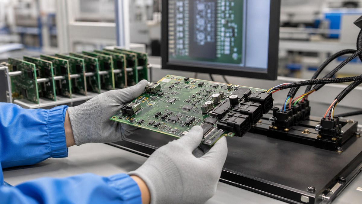
Teleoperation controller PCBA inspection with connector harness test fixture and assembled control boards
Connector, harness and functional-test planning should be part of the teleoperation PCBA build package.

Define programming access, bootloader method, firmware version control, fixture pins, current-limit settings, communication checks and pass/fail criteria. Test the board with expected cable lengths, antenna placement and representative actuator loads when possible. Supplier-side PCB test equipment should be discussed before volume builds if the project needs fixture-based functional testing, not after the pilot run exposes missing pads.

How should connectors, harnesses and enclosures be planned?

Connectors and harnesses should be placed around assembly access, strain relief, service direction, cable noise and enclosure sealing. Teleoperated products often fail mechanically before they fail electrically: vibration loosens cables, operator ports get stressed, or enclosure walls block connector access.

Check connector locking style, mating cycles, wire gauge, cable bend radius, shield termination, gasket clearance and mounting screw access. Keep high-current motor wiring away from RF and sensor lines where possible. If the supplier is expected to deliver a tested controller inside a housing, discuss Box Build Assembly requirements such as harness routing, enclosure labels, final test and packing constraints.

RFQ checklist for custom teleoperation PCB design

A useful RFQ package should show the supplier the control architecture, RF or wired link, power budget, motor loads, enclosure constraints and test requirements. Without those details, the quote may cover board fabrication but miss the risks that make a teleoperation product hard to build.

  1. Gerber files, drill files, netlist, stackup, copper weight and controlled revision number.
  2. Schematic, BOM, approved alternates, centroid file and assembly drawing.
  3. Communication method: RF module, antenna type, Ethernet, CAN, RS-485, USB, camera link or mixed interfaces.
  4. Power input range, battery or DC supply notes, maximum load current and motor-driver information.
  5. Connector drawings, harness direction, enclosure model, mounting holes and height limits.
  6. Programming method, firmware loading requirement and board-level functional-test criteria.
  7. Environmental notes such as vibration, dust, humidity, outdoor use, heat, chemical exposure or service access.
  8. Any components that require sourcing approval, lifecycle review or controlled substitutes.

Teleoperation products often depend on RF modules, processors, connectors, motor drivers, sensors and power ICs that cannot be swapped casually. Involve Component Sourcing before the pilot build if approved alternates, lifecycle status or lead-time risk could change the control behavior.

Supplier questions buyers should ask

Supplier questions should force a real engineering review of link reliability, power integrity, assembly risk and test coverage. A low unit price is not useful if the first build cannot be programmed, calibrated or tested under load.

  • Which layout areas are most likely to affect RF range, command response or feedback quality?
  • Are the antenna, connector and enclosure positions compatible with the communication method?
  • Do motor-driver current paths stay away from logic, RF and sensor feedback?
  • Are all programming, debug and functional-test pads reachable after assembly?
  • Which parts need approved alternates before production?
  • Can the test fixture simulate command input, feedback output and representative load current?
  • What should change before moving from engineering prototype to pilot production?

FAQ

What is custom PCB design for teleoperation?

Custom PCB design for teleoperation means designing a circuit board for remote command input, machine feedback, communication, power conversion, motor control, sensors and production test. The board must support predictable remote operation, not only basic robot movement.

Does teleoperation always need an RF PCB?

No. Some systems use wired Ethernet, CAN, RS-485 or tethered control. RF PCB review becomes important when the board includes antennas, wireless modules, controlled-impedance traces, coax connectors or tight enclosure constraints that affect radio performance.

What causes unstable teleoperation controller behavior?

Common board-level causes include motor noise coupling into logic, weak power rails, poor grounding, antenna placement problems, cable shielding mistakes, missing ESD protection, inaccessible test pads and firmware loading issues. Network software can also matter, but the PCB should not add preventable electrical faults.

How many layers should a teleoperation controller PCB use?

Simple prototypes may use two layers, but four or more layers are often safer when the board has RF, processors, motor drivers, cameras, sensors and many connectors. Planes help control return paths, EMI, routing density and power integrity.

What files are needed for a teleoperation PCB quote?

Send Gerber and drill files, schematic, BOM, centroid file, assembly drawing, stackup, enclosure notes, communication method, power budget, connector drawings and test requirements. Include firmware-loading and functional-test notes if the supplier will assemble the PCBA.

Conclusion

Custom PCB design for teleoperation should be reviewed around the full control path: command link, RF or wired interface, power rails, motor noise, sensor feedback, connectors, enclosure and test access. A supplier can quote more accurately when the RFQ includes the board files plus communication, power, harness and functional-test requirements. For a remote-control product, that preparation is often the difference between a board that only powers up and a controller that can be built, tested and improved repeatably.

You may also like

MIMO Antenna | RF PCB Layout, PCB Types, and Impedance Control
Wednesday, May 27th, 2026

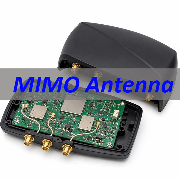
MIMO antenna is widely used in 5G CPE, LTE gateways, WiFi routers, IoT modules, UAV communication units, and industrial wireless devices. In these products, antenna performance is not only related to the antenna structure itself, but also to the PCB layout, RF trace consistency, connector reliability, controlled impedance, and PCBA assembly quality.

From a PCB and PCBA manufacturing point of view, the goal is not to redesign the antenna. The goal is to manufacture and assemble the board according to the customer’s approved RF layout, stackup, material, impedance, and assembly requirements.

Before fabrication, engineers and buyers should confirm several practical details, including RF trace width, PCB type, stackup, antenna keep-out area, controlled impedance, connector footprint, surface finish, BOM, pick-and-place file, and assembly drawing. For MIMO antenna PCB fabrication, RF PCB manufacturing, or PCBA assembly support, you can send your Gerber files, BOM, stackup, and assembly requirements to sales@bestpcbs.com for review and quotation.

MIMO antenna

What Is a MIMO Antenna?

A MIMO antenna is an antenna system that uses multiple antenna paths to send and receive wireless signals. MIMO stands for Multiple Input, Multiple Output. It is widely used in 5G, LTE, WiFi, IoT, industrial wireless devices, routers, gateways, UAV communication units, and smart electronic products.

For engineers and buyers, the key point is not only how the antenna works in theory. In a real product, the MIMO antenna is closely connected with the PCB layout, RF feed lines, grounding area, impedance control, connectors, and PCBA assembly quality.

A typical product using a MIMO antenna may include:

  • RF feed lines on the PCB
  • Printed antenna areas or external antenna connectors
  • Matching component pads
  • Controlled impedance traces
  • RF connectors such as SMA, IPEX, U.FL, or similar interfaces
  • Wireless module or chipset area
  • Ground reference and shielding clearance

From a PCB and PCBA manufacturing point of view, the role of the manufacturer is not to redesign the antenna. The real task is to produce the PCB and assemble the PCBA according to the customer’s approved RF layout, stackup, impedance, and assembly requirements.

For this reason, MIMO antenna projects should be reviewed carefully before fabrication. RF trace width, PCB stackup, antenna keep-out area, connector footprint, surface finish, and assembly files should all be checked early to reduce production risk.

2×2 MIMO Antenna vs 4×4 MIMO Antenna PCB

A 2×2 MIMO antenna usually uses two RF paths, while a 4×4 MIMO antenna uses four RF paths. For PCB manufacturing, this difference affects layout density, connector quantity, impedance control, and PCBA inspection.

Item2×2 MIMO Antenna PCB4×4 MIMO Antenna PCB
RF paths24
Layout densityLowerHigher
PCB space pressureLowerHigher
RF connectorsFewerMore
Matching componentsFewerMore
Controlled impedanceRequiredMore critical
PCBA inspectionModerateMore detailed

A 4×4 board usually needs more careful RF trace routing, connector placement, antenna spacing, and assembly checking. For compact devices, layout density should be reviewed early to reduce fabrication and assembly risks.

4×4 MIMO Antenna 5G PCB Requirements

A 4×4 MIMO antenna 5G board usually has tighter PCB space and more RF paths than a basic wireless board. This makes stackup, impedance control, and connector assembly more important.

Before production, these items should be reviewed:

Production ItemWhat to Confirm
PCB stackupDielectric thickness and layer structure
RF trace widthMatches the impedance calculation
Copper thicknessAffects etching and final impedance
Connector footprintSupports soldering and mechanical strength
Antenna areaKeep-out area is clear
Surface finishSuitable for RF connector soldering
PCBA filesBOM, placement file, and assembly drawing are complete

Most RF feed lines are designed around 50Ī© controlled impedance. The final trace width should be calculated based on the confirmed stackup, material data, copper thickness, and production tolerance.

LTE MIMO Antenna and 4G LTE MIMO Antenna PCB

An LTE MIMO antenna or 4G LTE MIMO antenna product often uses RF connectors, coaxial cables, module interfaces, or printed antenna areas. The PCB should support stable RF transmission and reliable assembly.

For LTE-related boards, the main manufacturing checks include:

  • RF trace width and clearance
  • Connector footprint accuracy
  • Ground reference near RF paths
  • Matching component pad size
  • Board edge accuracy if the antenna is near the outline
  • Surface finish for stable soldering
  • PCBA inspection for connectors and small RF components

For products using external LTE antennas, connector strength and cable direction should be checked before assembly. This helps reduce mechanical stress during final product installation.

MIMO WiFi Antenna PCB for Compact Devices

A MIMO WiFi antenna board is often used in WiFi 6, WiFi 7, router, gateway, smart home, and IoT products. These products usually have compact layouts, small RF components, and limited antenna space.

For compact WiFi boards, the PCB layout review should focus on:

  • Antenna keep-out area
  • RF trace continuity
  • Controlled impedance requirement
  • Ground clearance
  • Connector position
  • Component height near antenna areas
  • Shielding can clearance
  • Assembly access for inspection

Here, PCB layout support means manufacturability review and assembly review. It does not mean changing the customer’s full RF antenna design. The approved RF structure should be protected during PCB fabrication and PCBA assembly.

External MIMO Antenna Connections for PCB/PCBA

Many wireless products use an external MIMO antenna, such as a MIMO panel antenna, directional antenna, omnidirectional antenna, FPC antenna, or coaxial antenna interface. For a PCB and PCBA manufacturer, the focus is not to select the antenna type. The focus is to make sure the antenna connection on the PCB is accurate, reliable, and easy to assemble.

The connector area should be reviewed before production because it affects soldering strength, cable direction, enclosure fit, and long-term product reliability.

Antenna InterfacePCB/PCBA Focus
External MIMO antennaRF connector footprint, solder pad strength, and cable direction
MIMO panel antennaConnector position, enclosure clearance, and coax cable routing
MIMO directional antennaStable RF connector assembly and mechanical fixing
Omnidirectional MIMO antennaConnector layout, ground area, and assembly access
FPC antennaFPC connector soldering, cable bending direction, and fixture space
Coaxial antenna interfaceU.FL, IPEX, SMA, or similar connector footprint control

For PCBA production, RF connectors need careful inspection. Poor soldering, weak pad design, unsuitable plating, or tight cable bending may affect final assembly reliability. Before production, customers should confirm the connector type, footprint, cable direction, assembly drawing, and any mechanical clearance requirement.

PCB Types for MIMO Antenna Boards

Different wireless products may require different PCB types. The right choice depends on frequency, cost target, product size, impedance requirement, assembly structure, and reliability needs.

PCB TypeCommon UseManufacturing Focus
FR4 PCBBasic WiFi, IoT, and cost-sensitive wireless boardsMature process and cost-effective production
High-Tg PCBIndustrial wireless modules and long-running devicesBetter thermal stability
RF PCB5G, LTE, WiFi, and RF modulesImpedance, dielectric thickness, and RF trace control
Rogers PCBHigh-frequency and low-loss wireless productsStable dielectric performance for higher-frequency applications
Hybrid Stackup PCBRF + digital mixed circuitsBalances RF performance, cost, and structure
Rigid-Flex PCBSpace-limited wireless devicesSupports compact structure and reliable interconnection

For MIMO antenna PCB projects, PCB type selection should not be based only on price. It should match the RF path, stackup, impedance requirement, connector type, and PCBA assembly method.

Before production, these details should be confirmed:

  • PCB type
  • Material grade
  • Board thickness
  • Copper thickness
  • Stackup structure
  • Impedance requirement
  • Surface finish
  • Assembly method
  • Material availability

For RF-related projects, PCB type or material replacement should be handled carefully. Even when two options look similar, changes in dielectric constant, board thickness, copper type, or stackup may affect impedance result and production consistency.

MIMO Antenna PCB Layout and DFM Review

For this topic, PCB layout means layout support for manufacturability and assembly. It does not mean full antenna design or RF system redesign.

A practical DFM review should check whether the approved RF layout can be fabricated and assembled reliably.

Layout AreaDFM Review Point
Antenna keep-out areaNo unexpected copper, screws, cables, or tall components
RF feed lineShort, clean, and impedance-controlled
Ground areaStable ground reference and proper clearance
Matching component padsAccurate pad size and easy assembly
Connector placementSuitable for cable direction and inspection
Shielding areaEnough clearance from RF-sensitive areas
Board outlineCorrect mechanical fit and antenna edge control

For faster review, customers should provide Gerber files, PCB stackup, impedance requirement, BOM, pick-and-place file, assembly drawing, and RF notes.

MIMO Antenna PCB Manufacturing and PCBA Inspection

For MIMO antenna PCB manufacturing, the most important point is repeatability. A PCB supplier should help keep the same stackup, copper geometry, impedance result, and assembly quality from prototype to batch production.

Key manufacturing controls include:

Control ItemWhat to Check
Stackup controlDielectric thickness and layer structure
Controlled impedanceRF trace width, copper thickness, and tolerance
Etching accuracyRF trace shape and spacing
Board outlineAntenna edge and mechanical fit
Surface finishSolderability and connector reliability
Solder maskClearance around RF-sensitive areas
AOI inspectionTrace shape and copper defects
Electrical testContinuity and isolation
PCBA inspectionRF connector and matching component quality

For PCBA assembly, special attention should be given to:

  • RF connector soldering
  • Small matching components
  • Shielding can position
  • Coax cable direction
  • Connector mechanical strength
  • Cleanliness around RF areas
  • X-ray inspection when required

EBest Circuit supports PCB fabrication, RF board material selection, controlled impedance, DFM review, component sourcing, PCBA assembly, AOI, X-ray, electrical testing, and production follow-up for wireless electronic products.

FAQs About MIMO Antenna

Q1: What is a MIMO antenna?
A MIMO antenna uses multiple antenna paths to improve wireless speed, coverage, and connection stability.

Q2: What is a MIMO antenna PCB?
It is a PCB that carries antenna areas, RF feed lines, matching components, connectors, grounding areas, and related wireless circuits.

Q3: What is the difference between 2×2 and 4×4 MIMO antenna PCB?
A 2×2 board has two RF paths, while a 4×4 board has four. A 4×4 board usually needs more PCB space, better routing control, and more careful PCBA inspection.

Q4: What should be checked for a 4×4 MIMO antenna 5G PCB?
The stackup, RF trace width, impedance requirement, antenna keep-out area, connector footprint, surface finish, and assembly files should be checked before production.

Q5: Can FR4 be used for MIMO WiFi antenna PCB?
Yes. FR4 can be used for some WiFi and IoT products. For higher-frequency or lower-loss applications, RF PCB, Rogers PCB, or hybrid stackup PCB may be considered.

Q6: Does MIMO antenna PCB need controlled impedance?
Yes. RF feed lines usually require controlled impedance, commonly 50Ī©, to support stable RF transmission.

Q7: What PCB type is used for MIMO antenna boards?
Common options include FR4 PCB, High-Tg PCB, RF PCB, Rogers PCB, Hybrid Stackup PCB, and Rigid-Flex PCB. The choice depends on frequency, stackup, impedance, cost, and assembly structure.

Q8: What should be checked for external MIMO antenna connections?
RF connector footprint, solder strength, cable direction, mechanical clearance, plating quality, and PCBA inspection should be checked.

Q9: Can EBest Circuit manufacture MIMO antenna PCB and PCBA?
Yes. EBest Circuit can support MIMO antenna PCB fabrication, controlled impedance, RF material selection, DFM review, component sourcing, PCBA assembly, and testing. Send your Gerber, stackup, BOM, and assembly files to sales@bestpcbs.com for a quotation.

You may also like

RF Board
Friday, April 10th, 2026

What Is an RF PCB?

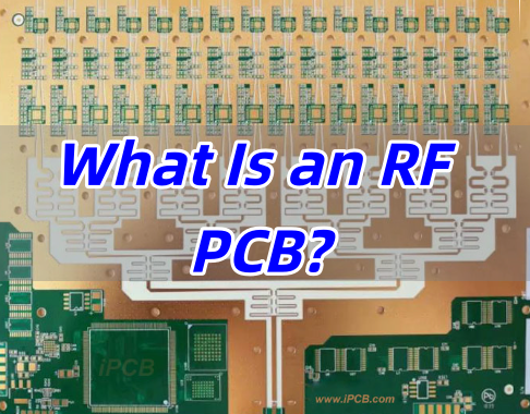
RF board, or Radio Frequency Printed Circuit Board, is engineered for circuits operating at high frequencies where signal integrity becomes highly sensitive to material properties. Typical RF designs work in the range of 300 MHz to 3 GHz, and many advanced systems extend far beyond this.

At these frequencies, standard FR4 materials often fail to maintain stable dielectric performance and low signal loss. As a result, specialized high frequency laminates are required. RF PCBs are therefore built using materials with low dielectric loss (Df) and stable dielectric constant (Dk) to ensure consistent signal transmission.

RF board is ideal for applications with higher operating frequency requirements. Right now, we normally use following material:

These boards are widely used in applications such as:

  • Wireless communication systems
  • RF antennas and modules
  • Automotive radar (ADAS)
  • Satellite and aerospace electronics
  • Microwave devices
  • IoT and high-speed signal systems

Why Use RF PCB Instead of Standard FR4?

FR4 is cost-effective and widely used, but its dielectric properties vary significantly at high frequencies. This leads to signal loss, impedance instability, and reduced system reliability in RF designs.

RF PCB materials solve these issues by offering:

  • Lower signal loss at high frequency
  • More stable dielectric constant across frequency range
  • Better impedance control
  • Reduced signal distortion
  • Improved phase consistency

What Materials Are Used in RF PCB?

Material selection is the core of RF PCB performance. Different applications require different dielectric properties and processing characteristics.

Common RF PCB Materials

1. Rogers Laminates

Widely used in RF and microwave circuits due to balanced performance and manufacturability.

Typical grades include:

  • RO4003C
  • RO4350B
  • RO4233

These materials offer:

  • Stable dielectric constant
  • Low loss tangent
  • Good thermal reliability

2. PTFE-Based Materials (Teflon)

Used in more demanding RF designs where ultra-low loss is critical.

Advantages:

  • Extremely low dielectric loss
  • Excellent high frequency performance

Considerations:

  • More complex processing
  • Higher manufacturing cost

Copper Thickness Range

  • Standard: 1/4 oz to 2 oz
  • Custom: based on current load and thermal design


Rogers is often the practical choice for most RF designs, while PTFE is used when performance requirements are more demanding.

Rogers Laminate Material Parameters

Choosing the right Rogers material directly affects signal integrity, impedance stability, and insertion loss. Below is a comparison of commonly used Rogers laminates for RF PCB applications.

MaterialDielectric Constant (Dk @10GHz)Loss Tangent (Df @10GHz)Thermal Conductivity (W/mĀ·K)Typical Application
RO4350B3.48 ±0.050.00370.62General RF, antennas, automotive radar
RO4003C3.55 ±0.050.00270.71RF communication, microwave circuits
RO42333.30 ±0.050.00250.65High frequency, low loss applications
RT58802.20 ±0.020.00090.20Ultra-low loss, aerospace, high-end RF
RO30033.00 ±0.040.00130.50High stability circuits, precision RF
RO301010.2 ±0.250.00230.95High dielectric designs, compact circuits

RF Board Capability

  • Base material: Rogers/Telfon
  • Board Thickness: 0.5mm~3.0mm(0.02″~0.12″)
  • Copper thickness: 0.5 OZ, 1.0 OZ, 2.0 OZ, 3.0 OZ
  • Outline: Routing, punching, V-Cut
  • Soldermask: White/Black/Blue/Green/Red Oil
  • Legend/Silkscreen Color: Black/White
  • Surface finishing: Immersion Gold, HASL, OSP
  • Max Panel size: 600*500mm(23.62″*19.68″)
  • Packing: Vacuum/Plastic bag
  • Samples L/T: 7~9 Days
  • MP L/T: 8~10 Days

RF PCB FAQs

1. What frequency requires RF PCB instead of FR4?

Typically, designs above 1 GHz or requiring strict impedance control should consider RF materials. Lower frequencies may still use FR4 depending on performance tolerance.

2. Is Rogers better than FR4?

For high frequency applications, yes. Rogers offers lower loss and more stable dielectric properties, which improves signal integrity.

3. Why is PTFE PCB more expensive?

PTFE materials are harder to process and require specialized manufacturing steps, which increases production cost.

4. Can RF PCB be used for mixed signal designs?

Yes. Hybrid stackups combining RF materials and FR4 are commonly used to balance performance and cost.

Start Your RF PCB Project Today

If you are designing RF or microwave circuits, choosing the right PCB is critical to performance.

At Best Technology, we combine material expertise, process control, and engineering support to deliver reliable RF PCB solutions.

📩 Send your design files to: sales@bestpcbs.com

Our engineering team will review your project and provide a fast quotation with optimization suggestions.

You may also like

2.4 GHz RF PCB Design & Prototype & Assembly | Fast Delivery, Custom Solutions
Tuesday, March 10th, 2026

What Is 2.4 GHz RF PCB?

A 2.4 GHz RF PCB is a high-frequency printed circuit board specifically engineered to transmit and receive radio signals within the 2.4 GHz ISM band. At this frequency, PCB traces no longer behave as simple copper conductors—they function as transmission lines. Every millimeter of trace length, dielectric variation, and copper geometry influences impedance, insertion loss, and radiation efficiency.

Unlike standard digital boards, a 2.4 GHz RF PCB requires controlled impedance (typically 50Ī©), stable dielectric materials, tight stackup tolerance, and precise grounding strategies. It is widely used in Bluetooth modules, WiFi systems, IoT gateways, wireless medical telemetry, industrial automation controllers, and aerospace communication subsystems.

What Is 2.4 GHz RF PCB?

Where Is 2.4 GHz RF PCB Used?

Common applications include:

  • Bluetooth modules
  • WiFi devices
  • Medical wireless monitors
  • Industrial IoT gateways
  • Aerospace telemetry systems

In aerospace communication boards, controlled impedance and low dielectric loss are mandatory. In medical telemetry PCBs, stable RF transmission ensures data reliability in patient monitoring systems.

Why Choose a Professional 2.4 GHz RF PCB Manufacturer Like EBest?

Because RF performance is extremely sensitive to material selection, impedance accuracy, and fabrication tolerance. A deviation of only ±0.1 in dielectric constant or slight stackup misalignment can detune antenna matching and reduce transmission efficiency.

A qualified 2.4 GHz RF PCB manufacturer must provide:

  • Controlled dielectric materials with verified Dk/Df values
  • Impedance modeling before fabrication
  • Tight copper thickness tolerance
  • RF-focused DFM review
  • TDR impedance verification

EBest offers custom RF PCB fabrication with impedance coupons, traceability, and integrated PCB + PCBA production. From prototype to mass production, RF consistency remains stable.

If you are developing IoT modules, Bluetooth devices, medical telemetry systems, or aerospace communication boards, selecting EBest ensures your RF performance remains predictable and repeatable.

What Are the Key Challenges in 2.4 GHz RF PCB Design?

At 2.4 GHz, traces behave as transmission lines. The primary challenge is impedance stability. A deviation of ±5% can reduce return loss margin and affect signal radiation efficiency.

Engineers often struggle with:

  • Microstrip vs stripline impedance selection
  • Antenna feed matching
  • Ground return discontinuities
  • Via stub resonance
  • Crosstalk between RF and digital layers

EBest mitigates these through pre-layout stackup planning, controlled dielectric selection, and DFM impedance modeling before production begins.

What Are the Key Challenges in 2.4 GHz RF PCB Design?

Why Is 2.4 GHz RF PCB Prototype So Difficult to Get Right?

Many early prototypes fail because material substitutes are used or dielectric thickness tolerance is ignored. At 2.4 GHz, even 0.1 mm dielectric shift changes impedance significantly.

Common prototype pain points:

  • Inconsistent material batch
  • Improper solder mask thickness
  • Poor antenna clearance
  • Unverified impedance coupon

EBest ensures prototype accuracy through:

  • Certified RF laminate sourcing
  • Controlled stackup tolerance
  • TDR impedance testing
  • RF DFM validation

If you need a reliable 2.4 GHz RF PCB prototype, we shorten development cycles while maintaining RF integrity.

What Are the Main Risks in 2.4 GHz RF PCB Assembly?

Assembly can alter RF behavior due to parasitic inductance and solder joint geometry.

Typical risks:

  • Excess solder altering impedance
  • Uneven ground stitching
  • Antenna detuning after reflow
  • Component placement affecting radiation pattern

EBest controls RF assembly through nitrogen reflow, controlled solder volume, and strict SMT placement tolerance. Your 2.4 GHz RF PCB assembly remains consistent from prototype to production.

What Are the Main Risks in 2.4 GHz RF PCB Assembly?

How Do You Control Impedance in a 2.4 GHz RF PCB?

Impedance is controlled by trace geometry, dielectric constant, and layer structure.

Impedance Control Comparison

ParameterMicrostripStripline
StructureOuter layerInner layer
EMI ExposureHigherLower
Manufacturing ComplexityModerateHigher
ApplicationAntenna feedShielded RF routing

What Materials Are Best for 2.4 GHz RF PCB?

Material selection determines signal loss and stability.

MaterialDkLoss TangentStabilityTypical Use
FR4~4.3ModerateStandardLow-cost IoT
Rogers 4350B~3.48LowHighRF modules
Hybrid (Rogers + FR4)MixedBalancedOptimizedCost-sensitive RF

For medical and aerospace systems, RF laminates or hybrid stackups provide improved signal stability.

How to Design Antenna Matching on 2.4 GHz RF PCB?

At 2.4 GHz, antenna matching is not optional—it directly determines radiation efficiency, range stability, and certification success. A poorly matched antenna can reduce effective radiated power, increase return loss, and cause unstable communication even if the RF chip itself performs correctly.

A well-designed 2.4 GHz RF PCB antenna section must ensure:

  • 50Ī© controlled feed line
  • Proper ground reference
  • Short and clean routing
  • Accurate impedance transition
  • Minimal parasitic inductance

Let’s break it down step by step.

1. Start With a True 50Ī© Feed Line

The antenna feed trace must maintain 50Ī© characteristic impedance from the RF transceiver output to the antenna input pad.

This requires:

  • Correct trace width based on dielectric constant
  • Consistent dielectric thickness
  • Continuous ground plane underneath

Even small deviations in trace width (for example ±0.05 mm) can shift impedance enough to affect matching. Use impedance calculation tools during layout and confirm with manufacturer stackup data.

2. Maintain a Continuous Ground Plane

The return current for RF signals flows directly beneath the signal trace. Any ground discontinuity creates impedance variation.
Design rules:

  • No split planes under RF traces
  • Avoid crossing gaps or power islands
  • Stitch ground vias near transitions
  • Keep via spacing short near antenna feed

Ground stitching vias placed near the antenna feed improve return path integrity and reduce unwanted radiation.
3. Keep the Antenna Trace Short and Straight

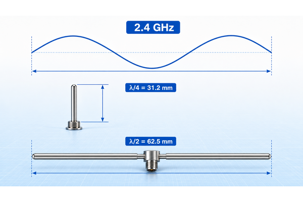
At 2.4 GHz, wavelength in free space is about 125 mm. On PCB substrate, the effective wavelength is shorter due to dielectric loading.

Design recommendations:

  • Avoid sharp 90° bends
  • Use smooth curves or 45° angles
  • Minimize trace length between RF chip and antenna
  • Avoid unnecessary test pads in RF path

Long feed traces introduce additional insertion loss and phase shift.

4. Design an Adjustable Matching Network

Most 2.4 GHz RF PCBs include a π-network (three-component matching circuit) between the RF chip and antenna.

Typical configuration:

  • Series inductor
  • Shunt capacitor to ground
  • Optional second capacitor

This allows tuning during prototype testing using a vector network analyzer (VNA).

5. Keep Antenna Clearance Area Clean

For PCB antennas (inverted-F, meandered, monopole), copper clearance around the antenna region is critical.

Best practices:

  • No ground copper under antenna radiator area
  • Maintain keep-out region recommended by antenna design
  • Avoid metal components nearby
  • Keep high-speed digital traces away

In medical and industrial designs, enclosure proximity must also be considered during layout.

6. Validate With S-Parameter Measurement

After fabrication, measure:

  • Return loss (S11)
  • VSWR
  • Bandwidth
  • Resonance frequency

Target values:

  • S11 < -10 dB at 2.4 GHz
  • VSWR < 2

If tuning is required, adjust matching network component values.

How Does 2.4 GHz RF PCB Affect Signal Integrity?

At 2.4 GHz, signal integrity is dominated by transmission line behavior rather than simple connectivity. The PCB layout itself determines reflection, loss, and radiation balance.

1. Reflection Due to Impedance Mismatch

If trace impedance differs from 50Ī©:

  • Part of the signal reflects back
  • Return loss degrades
  • Power transfer efficiency drops

Common causes:

  • Incorrect trace geometry
  • Ground discontinuity
  • Poor via transition

Controlled impedance fabrication and TDR testing reduce mismatch risk.

2. Insertion Loss Along the RF Path

Insertion loss increases with:

  • Trace length
  • Dielectric loss tangent
  • Copper roughness
  • Multiple vias

Low-loss materials reduce attenuation. Keeping RF traces short improves transmission margin.
3. Crosstalk From Digital Circuits

Digital switching noise can couple into RF traces.

Mitigation strategies:

  • Physical separation between RF and digital areas
  • Dedicated ground reference
  • Avoid parallel routing with clock lines
  • Use stripline for sensitive routing if needed

Industrial automation boards with strong EMI environments require strict partitioning.

4. Via Stub Resonance

Through-hole vias create unused stubs that may resonate near GHz frequencies.

Solutions:

  • Back-drilling
  • Blind or buried vias
  • Minimize via count in RF routing

Reducing via length improves S-parameter stability.

5. EMI and Certification Stability

Poor RF layout can cause unintended radiation, leading to compliance failures.

Proper stackup, clean return paths, and shielding integration reduce EMI risk—particularly important in medical electronics and aerospace communication modules.

2.4 GHz RF PCB Stackup Guidelines

Stackup structure directly influences impedance stability and EMI performance. At 2.4 GHz, the PCB layer arrangement becomes part of the RF system.

Recommended 4-Layer Stackup

LayerFunctionEngineering Purpose
L1RF SignalControlled 50Ī© routing
L2Solid GroundStable return path
L3Power PlaneIsolated supply distribution
L4Digital SignalsNoisy circuitry separation

Placing RF traces on the outer layer above a continuous ground plane simplifies impedance control and reduces loop inductance.

How Does 2.4 GHz RF PCB Affect Signal Integrity?

At 2.4 GHz, signal integrity is dominated by transmission line behavior rather than simple connectivity. The PCB layout itself determines reflection, loss, and radiation balance.

1. Reflection Due to Impedance Mismatch

If trace impedance differs from 50Ī©:

  • Part of the signal reflects back
  • Return loss degrades
  • Power transfer efficiency drops

Common causes:

  • Incorrect trace geometry
  • Ground discontinuity
  • Poor via transition

Controlled impedance fabrication and TDR testing reduce mismatch risk.

2. Insertion Loss Along the RF Path

Insertion loss increases with:

  • Trace length
  • Dielectric loss tangent
  • Copper roughness
  • Multiple vias

Low-loss materials reduce attenuation. Keeping RF traces short improves transmission margin.


3. Crosstalk From Digital Circuits

Digital switching noise can couple into RF traces.

Mitigation strategies:

  • Physical separation between RF and digital areas
  • Dedicated ground reference
  • Avoid parallel routing with clock lines
  • Use stripline for sensitive routing if needed

Industrial automation boards with strong EMI environments require strict partitioning.

4. Via Stub Resonance

Through-hole vias create unused stubs that may resonate near GHz frequencies.

Solutions:

  • Back-drilling
  • Blind or buried vias
  • Minimize via count in RF routing

Reducing via length improves S-parameter stability.

Why Fast Turn 2.4 GHz RF PCB Manufacturing Matters?

Wireless product development cycles are often short. Engineers need quick prototypes to test antenna performance and communication reliability.

Fast manufacturing helps accelerate development and reduce time to market.

Rapid production offers several advantages:

  • Faster prototype validation
  • Earlier detection of design issues
  • Shorter development cycles
  • Improved product launch timing

EBest (Best Technology) provides professional 2.4 GHz RF PCB fabrication, prototype manufacturing, and RF PCB assembly services for wireless products in industries such as medical electronics, aerospace communication systems, and industrial IoT equipment.

Our engineering team works closely with customers to optimize RF layout, impedance control, and antenna performance.

If you need reliable 2.4 GHz RF PCB manufacturing, feel free to contact us.

Email: sales@bestpcbs.com

We are ready to support your next wireless electronics project.

You may also like

Are RF PCB and High-Frequency PCB the Same?
Tuesday, December 9th, 2025

Not exactly. All RF PCBs fall under the high-frequency PCB category, but not all high-frequency PCBs qualify as RF PCBs.

RF PCB work sits at the center of many wireless systems, and an RF PCB often looks similar to a high frequency pcb. Many designers ask if they are the same board. They are related, yet each one handles different needs in signal flow, layout control, and material behavior.

As we move deeper into 5G, radar modules, and clean wireless designs, the differences become more visible. This article explains those differences in simple, clear language. More importantly, it guides engineers, buyers, and project teams on how to choose the right board for their next product.

What Is an RF PCB?

An RF PCB full name is Radio Frequency PCB, which is specifically handles signals in the radio frequency range: typically 300 MHz to 300 GHz, including microwave and millimeter-wave designs.

RF PCBs involve much stricter engineering constraints:

  • Tight impedance (<±5%) on microstrip, grounded CPW, stripline
  • Precise feature control (trace width tolerance around ±0.01–0.03 mm)
  • Stable dielectric properties across temperature
  • Very low-loss materials such as RO3003, RO4350B, RO5880, Taconic RF-35, PTFE woven/non-woven
  • Specialized stackups to avoid parasitic radiation
  • Careful via design to avoid stubs and resonance

Applications include:

  • Radar systems
  • Satellite communication
  • LNBs
  • RF front-end modules
  • Power amplifiers
  • Filters, couplers, antennas

RF PCB is wider use of 5G, IoT, and compact antennas has created strong demand for high-grade rf pcb builds. Because the signals travel along microstrip or CPW structures, the board behaves like part of the RF device, not only a carrier.

What Is a High-Frequency PCB?

A high-frequency PCB is any printed circuit board operating above roughly 500 MHz to 10 GHz+, depending on the design community.

These boards focus on:

  • Stable dielectric constant (Dk tolerance ±0.02–0.05)
  • Low dissipation factor (Df) for reduced signal loss
  • Good impedance control across long traces
  • Suitable materials like Rogers RO4003C, RO4350B, RO3003, PTFE, Isola I-Tera MT40, etc.

High-frequency PCBs serve applications such as:

  • 5G modules
  • Wi-Fi devices
  • GPS receivers
  • High-speed digital layouts (DDR4/DDR5, SerDes)

High frequency boards focus on clean rise times, controlled impedance, and manageable dielectric loss. They support Wi-Fi, Bluetooth, high-speed digital lines, and mixed-signal designs. The design margin is wider than rf pcb work because the board deals with digital pulses, not pure RF energy.

high frequency pcb

High Frequency PCB

Key Differences Between RF PCB vs. High Frequency PCB

AspectHigh-Frequency PCBRF PCB
DefinitionBoards operating at high digital or analog frequenciesBoards designed specifically for RF signal transmission
Signal Range500 MHz–10 GHz+300 MHz–300 GHz
Design FocusSignal integrity, low lossElectromagnetic control, transmission lines, matching
MaterialRogers 4000 series, Isola, Panasonic MegtronPTFE, RO3003/5880, ceramic-filled laminates
Impedance ControlImportantCritical (tighter tolerance)
Manufacturing DifficultyMediumHigh
Typical UseWi-Fi, Bluetooth, high-speed digitalRadar, RF amplifiers, filters, GNSS, mmWave

When Are They ā€œthe Same PCBā€?

A design can fall under both categories when:

  • The signal is RF (e.g., 2.4 GHz, 5.8 GHz)
  • The designer uses high-frequency materials
  • The board contains microstrip, CPW, filters, or antennas

For example, a 2.4 GHz RF transceiver board using RO4350B is simultaneously:

  • a high-frequency PCB, because frequency is high
  • an RF PCB, because it processes RF signals

Thus, overlap exists, but they are not inherently identical.

Which One Should You Specify to Your PCB Supplier?

If your project handles RF transmission, always specify RF PCB so the manufacturer focuses on:

  • surface roughness control (Ra < 2 µm for low loss)
  • uniform dielectric thickness
  • controlled resin flow during lamination
  • tighter etching tolerance
  • Dk matching for microstrip/CPW accuracy

If it is only high-speed digital (e.g., PCIe, SerDes), then choose high-frequency PCB.

Why Do RF PCBs Need Special Materials Compared with High Frequency PCBs?

Material behavior influences both categories. Yet an rf pcb is more sensitive to the dielectric constant and copper profile.

RF units run energy through transmission lines. If the copper roughness increases loss, the system sees reduced range or gain shift. If the Dk drifts, the phase response moves. Because of this, the most common materials for rf pcb work include RO3003, RO4350B, RO5880, and PTFE blends.

In contrast, high frequency pcb materials can include Megtron series or Rogers 4000 series because the signal shape is less sensitive to phase stability. They still target low loss, but their working window is wider.

Why Do RF PCBs Need Special Materials Compared with High Frequency PCBs?

What Frequencies Define RF PCB Work vs High Frequency PCB Work?

Both ranges relate to how the signal behaves. RF work usually starts at 300 MHz and goes up to millimeter-wave. This includes radar, satellite, GPS, 24 GHz and 77 GHz systems, and many short-range radios.

High frequency ranges start from about 500 MHz to beyond 10 GHz. These support fast digital buses, Wi-Fi, and mixed-signal designs.

However, the frequency alone does not decide the board’s category. The final system function does.

Do RF PCBs Always Cost More Than High Frequency PCBs?

Actually yes when under the same design. RF boards use premium materials. These materials cost more because they hold stable Dk, low loss, and a smooth copper surface. They also require strict process control during drilling, plating, and lamination.

High frequency boards may use moderate-cost materials such as RO4003C or Megtron 4. They also need controlled lamination, yet the window for yield is wider.

Costs also rise when an rf pcb uses fine lines, tight impedance, or stacked microstrip structures. That said, skilled manufacturers can keep RF costs under control by optimizing stackup and process flow.

What Problems Occur When Designers Use the Wrong PCB Type?

If a design intended for RF is built on a standard high frequency pcb, several issues may appear:

  • Reduced communication range
  • Higher insertion loss
  • Unstable gain
  • Incorrect antenna tuning
  • Phase delay changes
  • EMC issues

Although not every situation is severe, these issues waste time in testing and rework.

When a high frequency digital board is produced using strict RF rules, the design remains stable. Yet the cost often rises without a visible performance gain.

What Tests Are Important for RF PCBs Compared with High Frequency PCBs?

RF boards often need tests beyond regular PCB checks. These include:

  • Dielectric thickness check
  • Dk variation review
  • Copper profile check
  • TDR impedance scan
  • S-parameter review after assembly

High frequency boards may also use TDR scans, yet the tolerance is wider. For RF, every shift affects the final device.

How Does EBest Circuit (Best Technology) Support RF PCB and High Frequency PCB Projects?

EBest Circuit (Best Technology) offers full material guidance, stackup review, transmission line advice, and strong quality assurance for both rf pcb and high frequency pcb builds. We handle small prototype lots and volume orders with the same care. Each rf pcb passes a detailed review, so the final product meets the performance target.

Our strengths include:

  • ISO9001, ISO13485, IATF16949, and AS9100D systems
  • Complete MES traceability
  • Tight impedance control
  • Fine etching for RF lines
  • Skilled process teams for PTFE and hybrid stackups
  • Smooth copper profile management
  • Fast prototype to mass build for global clients

We support antenna work, radar modules, filters, amplifiers, and mixed-signal boards. Our engineering team reviews each design before production to catch layout risks early to speed up product launches. For your next RF or high frequency project, our team stands ready to guide you from concept to delivery!

FAQs

1. Is an rf pcb the same as a high frequency pcb?

No. All RF boards are high frequency boards, but not all high frequency boards meet RF conditions.

2. Can I use RO4003C for both RF and high frequency PCB use?

Yes. However, many RF systems still need lower-loss materials such as RO3003 or RO5880.

3. Are RF boards harder to build?

Yes. They need tighter process control, smoother copper, and stable lamination.

4. How do I know if my design needs an rf pcb?

If your design uses antennas, filters, couplers, or PA modules, you need an RF board.

5. Does EBest Circuit (Best Technology) support RF and high frequency PCBA work?

Yes. We handle full assembly, tuning, connector installation, and testing.

You may also like

High Frequency PCB Design Guidelines – RF PCB Basic Acknowledge
Wednesday, August 20th, 2025

Are you often curious about these questions about high frequency PCB?

  • Have you ever wondered why some electronic systems lose performance at higher frequencies?
  • Why a well-designed PCB for low-speed circuits often fails when pushed into GHz ranges?
  • How can designers minimize losses above 1 GHz?

The answer lies in the design of high frequency PCBs. High frequency PCBs also known as RF PCB or radio frequency pcb. They are more important in applications such as 5G, automotive radar, aerospace communication, medical imaging, and satellite systems. These boards must handle signals above 100 MHz and, in many cases, well into the GHz range. At such speeds, signal losses, impedance mismatches, and electromagnetic interference (EMI) can cause severe degradation.

This blog provides detailed guidelines for designing high frequency PCBs. From material selection to signal routing, impedance control, thermal management, and testing, we will walk through the critical factors engineers must consider.

What Frequency Range is Considered High Frequency in PCB Design?

In PCB engineering, high frequency generally refers to signal frequencies above 500 MHz. For RF and microwave circuits, the range extends from 1 GHz up to 100 GHz. Typical applications include:

  • Wi-Fi (2.4 GHz / 5 GHz)
  • Bluetooth (2.4 GHz)
  • 5G NR bands (3.5 GHz / 28 GHz / 39 GHz)
  • Automotive radar (24 GHz / 77 GHz)
  • Satellite communication (Ku-band 12–18 GHz, Ka-band 26–40 GHz)

The higher the frequency, the more sensitive the PCB becomes to signal loss, dielectric constant stability, and copper surface roughness. For instance, at 28 GHz (5G mmWave), even 0.1 dB/cm of insertion loss can cause serious degradation in system performance.

High Frequency PCB Design Guidelines - RF PCB Basic Acknowledge

What PCB Materials are used for High Frequency Applications?

The dielectric substrate is the foundation of high frequency PCB design. Key material properties include:

  • Dielectric Constant (Dk): Should remain stable across frequency and temperature.
  • Dissipation Factor (Df): Lower values mean lower signal loss.
  • Thermal Conductivity: Crucial for high-power RF designs.

Common Materials for High Frequency PCBs

Material TypeDielectric Constant (Dk)Dissipation Factor (Df) @10GHzThermal Conductivity (W/mĀ·K)Typical Use Case
FR4 (High Tg)4.2–4.70.020–0.0250.3<1 GHz, low-cost boards
Rogers RO4350B3.48 ±0.050.00370.692–20 GHz, antennas
Rogers RO30033.00 ±0.040.00130.50mmWave 5G (28 GHz, 39 GHz)
Taconic RF-353.500.00180.62Microwave circuits
PTFE (Teflon)2.1–2.60.0009–0.00150.25–0.30Aerospace, radar
Ceramic-filled PTFE3.0–100.001–0.0050.7–1.2High-power RF

Data comparison shows that Rogers RO3003 has one of the lowest Df values, making it widely used in 5G mmWave base stations. PTFE-based laminates dominate satellite and radar applications where extreme performance is required.

How Does Dielectric Constant Affect Signal Speed?

The dielectric constant (Dk) directly influences the propagation velocity of signals on PCB traces. The relation is:

How Does Dielectric Constant Affect Signal Speed?

Where c = 3 Ɨ 10^8 m/s (speed of light in vacuum).

  • For FR4 (Dk ā‰ˆ 4.5) → v ā‰ˆ 1.41 Ɨ 10^8 m/s
  • For Rogers RO4350B (Dk ā‰ˆ 3.48) → v ā‰ˆ 1.61 Ɨ 10^8 m/s
  • For PTFE (Dk ā‰ˆ 2.2) → v ā‰ˆ 2.02 Ɨ 10^8 m/s

This means PTFE substrates allow signals to travel ~43% faster than FR4. In high-speed digital systems (like SerDes 56G PAM4 links), such differences greatly influence timing margins.

What are the Key Design Rules for High Frequency PCB Layout?

Designing high frequency boards requires stricter rules compared to conventional PCBs:

1. Controlled Impedance Traces

  • Single-ended 50 Ī©, differential 90–100 Ī© are typical.
  • Impedance tolerance must be within ±5% for frequencies above 10 GHz.

2. Insertion Loss Minimization

  • Use smooth copper foils (Ra < 2 μm).
  • Keep transmission lines short.
  • Avoid unnecessary vias, which can introduce 0.1–0.2 dB loss per via at 10 GHz.

3. Ground Plane Integrity

  • Solid reference planes reduce return path discontinuities.
  • Use via fences to confine RF energy.

4. Crosstalk Reduction

  • Maintain spacing ≄3Ɨ trace width between high frequency lines.
  • Place sensitive analog circuits far from digital noise sources.

5. Thermal Management

  • For power amplifiers, substrates with >0.8 W/mĀ·K thermal conductivity are recommended.
  • Use thermal vias under RF components for efficient heat dissipation.
What are the Key Design Rules for High Frequency PCB Layout?

How Thick should a High Frequency PCB be?

The thickness of the PCB substrate directly impacts impedance and signal integrity. Typical stack-up configurations:

PCB ThicknessLayer CountDielectric ThicknessFrequency Application
0.2–0.4 mm2–4L0.1 mm coreHigh-speed connectors, 10–20 GHz
0.6–0.8 mm4–6L0.2 mm core2.4/5 GHz Wi-Fi, Bluetooth
1.0–1.6 mm6–10L0.3–0.5 mm coreAutomotive radar, 24 GHz
2.0+ mm8–12L>0.5 mm core28 GHz 5G, satellite boards

For example, in 77 GHz automotive radar PCBs, manufacturers often use 0.254 mm or thinner substrates to reduce dielectric loss and keep microstrip lines narrow enough for impedance control.

How to Reduce Signal Loss in High Frequency PCB Design?

Signal loss (attenuation) is one of the biggest concerns in high frequency circuits. It is affected by:

  • Dielectric Loss: Higher Df increases insertion loss.
  • Conductor Loss: Surface roughness increases resistance at high frequencies due to skin effect.
  • Radiation Loss: Poor layout or sharp bends radiate energy.

Example of Insertion Loss Data

MaterialFrequencyLine LengthInsertion Loss
FR4 (Df 0.020)10 GHz10 cm-1.2 dB
Rogers RO4350B10 GHz10 cm-0.25 dB
PTFE (Df 0.001)10 GHz10 cm-0.05 dB

This demonstrates why high frequency applications almost never rely on standard FR4.

In Conclusion

Designing a high frequency PCB requires more than standard PCB know-how. From material selection to impedance control, routing, thermal management, and advanced testing, every step must be carefully engineered.

EBest Circuit (Best Technology) is a trusted PCB manufacturer in China with expertise in high frequency PCB fabrication. We offer advanced laminates like Rogers, Taconic, and Isola, alongside ISO9001, ISO13485, IATF16949, and AS9100D certifications. Our team applies rigorous quality control, competitive pricing, professional engineering support, and MES-based traceability to deliver reliable high frequency PCBs for industries such as 5G, automotive radar, medical devices, and aerospace.

If your project requires precise high frequency PCB solutions, EBest Circuit (Best Technology) is ready to provide professional guidance and manufacturing excellence.

FAQs

1. Can FR4 be used for high frequency PCBs?

Yes, but only for frequencies below ~1 GHz. For anything higher, specialized laminates are required.

2. What is the most commonly used material for 5G PCBs?

Rogers RO4350B and RO3003 are widely adopted due to their low loss at mmWave bands.

3. How do vias affect high frequency performance?

Each via can add 0.1–0.2 dB loss at 10 GHz, so designers minimize via count in RF paths.

4. Why is surface roughness important?

At high frequencies, the skin effect confines current to the outer conductor surface. Rough copper increases resistance and loss.

You may also like

RF Circuit Board For Anti Drone System
Saturday, July 12th, 2025

How can RF circuit board revolutionize anti-drone systems with their unique capabilities? This overview explores their design principles, environmental resilience, cost-efficiency, and full-band performance in counter-drone applications.

  • How to achieve an effective interference distance of 500 meters with a limited budget?
  • How to avoid signal interference causing false alarms from communication base stations?
  • Can it be compatible with mainstream drone frequency bands without interfering with GPS?

EBest Circuit (Best Technology) Can Provide You:

  • Stepped power enhancement service: Dynamic impedance matching technology improves antenna efficiency, and actual measurements show that it can extend the effective interference distance by 15%.
  • Base station signal collaborative analysis service: Adaptive notch filter is used to achieve 20ms-level rapid response to sudden base station signals.
  • Multi-protocol compatible solution: GPS L1 band out-of-band suppression reaches 55dB, and millimeter-level frequency band isolation is achieved through cavity filters.

Welcome to contact us if you have any request for RF circuit boards: sales@bestpcbs.com.

What Is A RF Circuit Board?

A RF circuit board is a specially engineered printed circuit board designed to transmit, receive, and process high-frequency radio signals, typically from a few megahertz (MHz) into the gigahertz (GHz) range and beyond. Unlike standard PCBs handling lower frequencies or digital signals, these boards require exceptional attention to signal behavior at high speeds.

They utilize specialized dielectric materials, such as PTFE (Teflon) or ceramic-filled laminates, chosen for stable electrical properties and minimal signal loss at RF frequencies. Precise control over trace geometries, impedance matching, grounding structures (like coplanar waveguides), and shielding techniques are fundamental. This careful design minimizes signal distortion, power loss (insertion loss), and unwanted radiation (EMI), ensuring signal integrity is maintained throughout the circuit path. RF circuit boards are essential components in wireless communication devices, radar systems, satellite technology, and high-speed test equipment.

What Is A RF Circuit Board?

Benefits of RF Circuit Boards

  • Superior High-Frequency Handlingā€Œ: RF circuit boards maintain signal quality across wireless frequencies from mobile networks to satellite communications, preventing degradation.
  • Precision Signal Managementā€Œ: Advanced designs minimize interference between components, ensuring stable connections in crowded electronic environments.
  • Temperature-Resistant Operationā€Œ: Specialized materials prevent performance fluctuations during extended use or in extreme conditions.
  • Space-Efficient Architectureā€Œ: Multi-layer construction allows complex circuitry in compact devices like wearables and IoT sensors.
  • Enhanced Durabilityā€Œ: Manufactured to withstand environmental stressors including moisture, vibration, and thermal cycling.
  • Application-Specific Customizationā€Œ: Engineers can optimize designs for particular frequency ranges, power requirements, and physical constraints.
  • Energy-Efficient Performanceā€Œ: Optimized signal pathways reduce power waste, extending battery life in portable electronics.
Benefits of RF Circuit Boards

Application of RF Circuit Board

  • 5G RF Boards – Enable low-latency millimeter-wave data transfer in urban networks.
  • Medical RF Systems – Process high-precision signals for MRI/radiotherapy with thermal stability.
  • Automotive Radar Modules – Support 77 GHz collision detection and adaptive cruise control.
  • Satellite RF Components – Manage X/Ka-band signals for GPS and Earth observation in space.
  • IoT RF Connectivity – Provide Bluetooth/Wi-Fi links in smart devices with compact, low-power designs.
  • Military RF Tech – Jam signals and analyze spectrums with EMI-shielded high-power amplifiers.
  • Industrial RF Control – Enable wireless robot/AGV operation via interference-resistant frequency-hopping.
  • Consumer Electronics RF – Integrate cellular/Wi-Fi/GPS in smartphones with miniaturized, high-efficiency layouts.

How to Design RF Circuit Boards for Anti-Drone Jamming Systems?  

RF Circuit Board Design Process for Anti-Drone Jamming Systems:

1. Architectural Design

  • Split into transmit (TX) and receive (RX) modules.
  • Map RF signal flow from amplifiers to antennas.

2. Component Selection

  • Amplifiers: GaN transistors (2–6 GHz) with OIP3 > 45 dBm.
  • Filters: Cavity filters (TX) and SAW filters (RX).
  • Antennas: Directional patch arrays (≄15 dBi gain) with circular polarization.

3. PCB Layout

  • Layer Stackup: 6-layer board with RF layers between ground planes.
  • Impedance Control: 50 Ī© microstrip traces (Er = 3.5–4.5).
  • Isolation: Separate TX/RX sections by ≄50 mm; use via fences (20 mils diameter).

4. Power & Thermal Design

  • Power: DC-DC converters (≄90% efficiency); twisted-pair cables.
  • Thermal: Aluminum heat sinks with thermal epoxy; NTC thermistors.

5. Signal Integrity & EMC

  • Routing: High-power traces ≄3Ɨ wider than low-level signals.
  • Shielding: Aluminum enclosures with EMI gaskets; stitched vias.
  • Grounding: Star topology; M3 screws for chassis-to-board grounding.

6. Prototyping

  • Fabricate 4-layer board with tunable component footprints.
  • Include SMA connectors for temporary testing.

7. Validation

  • Lab Testing: Measure power, harmonics, and EVM using VNA.
  • Field Testing: Deploy in open areas; monitor interference with spectrum analyzers.
How to Design RF Circuit Boards for Anti-Drone Jamming Systems? Ā 

How to Ensure Extreme Environmental Reliability in Anti-Drone RF Boards?

Optimized Strategies for Extreme Environmental Reliability in Anti-Drone RF Boards:

Robust Material Selection

  • Use high-Tg laminates (e.g., PTFE, ceramic-filled hydrocarbons) for substrates to resist thermal deformation.
  • Apply thick copper traces (≄2 oz) to minimize resistive losses under temperature extremes.

Advanced Thermal Management

  • Integrate thermal vias (12 mils diameter, 8 mils spacing) under power amplifiers to transfer heat to ground planes.
  • Attach aluminum/copper heat sinks with phase-change materials (PCMs) for low-resistance bonding.
  • Include Peltier modules or fans for forced-air cooling in enclosed systems.

Environmental Sealing

  • Apply conformal coatings (acrylic, silicone, or parylene, 25–50 µm) to protect against moisture and chemicals.
  • Encapsulate critical components in epoxy/urethane potting for shock and vibration resistance.
  • Use silicone/EPDM gaskets around connectors for IP67/IP68 compliance.

Vibration and Shock Mitigation

  • Replace rigid connectors with flexible PCBs or shielded cables to absorb mechanical stress.
  • Secure heavy components with epoxy adhesive or locking screws.
  • Attach boards to chassis using rubber or spring-loaded standoffs for vibration damping.

Corrosion and Humidity Control

  • Apply ENIG or OSP finishes to pads and vias for corrosion resistance.
  • Use sacrificial zinc coatings on metal enclosures in salt-fog environments.
  • Include desiccant packets inside sealed enclosures to manage humidity.

Extreme Temperature Adaptation

  • Select components rated for -55°C to +125°C operation (capacitors, resistors, inductors).
  • Use Sn-Bi or Sn-Ag-Cu solder alloys (melting point <140°C) to prevent cold-environment cracking.

EMI/EMC Hardening

  • Enclose RF sections in nickel-silver or copper shields with EMI gaskets.
  • Add feedthrough capacitors and ferrite beads to power lines for noise suppression.
  • Implement single-point grounding for analog and digital sections to avoid loops.
How to Ensure Extreme Environmental Reliability in Anti-Drone RF Boards?

Cost-Effective RF Circuit Board Solutions for Anti-Drone System

Component Standardization

  • Use COTS amplifiers/filters (e.g., 2.4 GHz/5.8 GHz modules) to eliminate custom development costs.
  • Replace discrete components with integrated front-end modules (amplifier + filter combinations).

Material Optimization

  • Use FR-4 substrates for non-RF sections (e.g., control logic) to cut material expenses by 30–50%.
  • Reserve PTFE/ceramic laminates only for high-frequency traces (e.g., antenna feeds).

Simplified Layer Stackup

  • Design 4-layer boards (signal-ground-power-ground) instead of 6-layer.
  • Avoid blind/buried vias; use through-hole vias with staggered patterns for cost efficiency.

Automated Testing

  • Develop in-house test jigs (e.g., Arduino-based power meters) for basic checks (output power, harmonics).
  • Replace expensive spectrum analyzers with open-source tools (e.g., GNU Radio scripts) for signal validation.

Design Reuse

  • Create modular sub-boards (e.g., 2.4 GHz power amplifier module) repurposable across systems.
  • Standardize connectors (e.g., U.FL for RF, JST for power) to simplify inventory and repairs.

Thermal Management Trade-offs

  • Replace active cooling (fans, Peltier modules) with passive solutions (aluminum heat sinks + thermal pads).
  • Use stamped aluminum enclosures instead of machined magnesium for 40–60% cost reduction.

Regulatory Compliance

  • Pre-certify designs for unlicensed bands (e.g., 2.4 GHz Wi-Fi) to avoid redesign costs.
  • Use pre-compliance tools (e.g., USB spectrum analyzers with EMI filters) before formal testing.

Lifecycle Cost Reduction

  • Design for field repairability (socketed amplifiers, plug-in filters) to extend device lifespan.
  • Update firmware via USB/SD cards instead of hardware recalls (50–70% savings per update).

Why Choose EBest Circuit (Best Technology) as Your RF Board Manufacturer?

  • High-Frequency Precision Manufacturing – With ±0.025mm drilling accuracy and impedance control within 1%, we solve signal integrity issues in 5G/mmWave designs, backed by 67GHz testing.
  • Material & Process Expertise – 50+ qualified laminates (including ultra-low-loss Rogers/Duroid) and strict tan Ī“ (<0.0015) control ensure consistent RF performance.
  • Thermal Reliability Solutions – Metal-core boards and embedded heat pipes (15W/cm² dissipation) prevent warping/delamination in high-power applications.
  • Rapid Prototyping & NPI Support – 24 hours prototype turnaround with DFM feedback within 4 hours accelerates your development cycle.
  • Supply Chain Security – 12-month buffer stock of critical materials and AS9100 logistics eliminate production delays.
  • Dedicated Engineering Partnership – Each project gets a senior RF engineer for real-time technical support from design to volume production.

Can RF Boards Overcome Full-Band Scanning Failures?

Yes, RF boards can overcome full-band scanning failures through design optimizations, signal processing, and environmental hardening. These strategies ensure reliable spectrum analysis even in noisy or dynamic conditions.

Signal Integrity Focus

  • Use impedance-matched microstrip lines (50 Ī© ±5%) and via stitching to minimize signal loss, ensuring weak frequencies are detected during scans.
  • Integrate bandpass filters (e.g., SAW) to suppress out-of-band interference, improving signal clarity.

Dynamic Range Management

  • Deploy low-noise amplifiers (LNAs) with <1 dB noise figures to amplify faint signals without distortion.
  • Add automatic gain control (AGC) to adjust amplification levels dynamically, preventing saturation from strong nearby signals.

Redundant Scanning Paths

  • Design multi-channel architectures (e.g., dual independent receivers) to cross-validate results, reducing false negatives from single-channel issues.
  • Use RF switches to reroute signals to backup channels if anomalies are detected, ensuring continuous scanning.

Environmental Stability

  • Include temperature sensors and bias-adjustment circuits to stabilize amplifier performance across -40°C to +85°C, avoiding thermal drift.
  • Shield sensitive components (e.g., LNAs) with nickel-silver enclosures and EMI gaskets to block external interference.

Adaptive Software Tools

  • Embed self-calibration routines (e.g., frequency sweeps) to compensate for component aging or manufacturing variances.
  • Use FPGA-based processing to adjust scan parameters (dwell time, step size) in real time based on environmental feedback

By combining these approaches, RF boards deliver robust full-band scanning capabilities, making them reliable for anti-drone systems, spectrum monitoring, and wireless security applications.

You may also like