PCB manufacturing PCB manufacturing
Home > Blog

microvias

HDI PCB Fabrication Guide: Stackups, Microvias, Process, and Cost
Friday, July 10th, 2026

Smaller components and finer-pitch packages have changed how engineers route multilayer PCBs. A conventional through-hole structure may work well for a 0.8 mm-pitch BGA, but it often becomes restrictive once the pitch drops to 0.5 mm, 0.4 mm, or below.

That is where HDI PCB fabrication becomes useful. A high-density interconnect PCB uses microvias, thin dielectric layers, smaller pads, and sequential lamination to create more routing channels within a limited area. It also adds laser drilling, via filling, tighter registration, and additional lamination work.

What Is HDI PCB Fabrication?

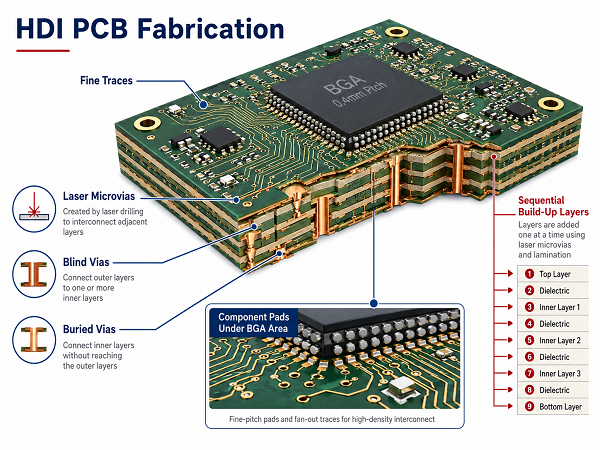
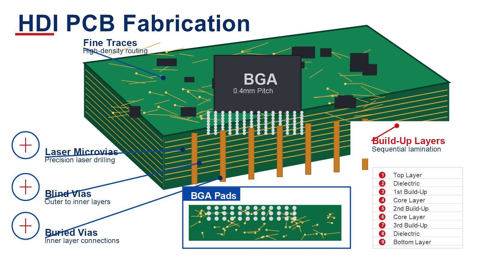
HDI PCB fabrication is the manufacture of printed circuit boards with a higher wiring density than standard multilayer boards. Common HDI features include:

  • Laser-drilled microvias
  • Blind and buried vias
  • Fine trace and space
  • Small capture pads
  • Thin dielectric layers
  • Via-in-pad structures
  • Sequential lamination
  • Stacked or staggered microvias

HDI is useful when a design must escape signals from a fine-pitch BGA, reduce board size, shorten interconnections, or increase routing density without adding an excessive number of layers.

It is often unnecessary when the PCB has enough routing space, uses larger-pitch packages, and can be completed with standard through-holes. In that case, a conventional multilayer PCB is usually more economical.

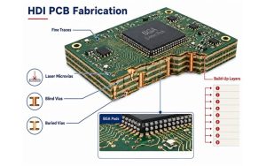
HDI PCB Fabrication

How Is an HDI PCB Different from a Conventional Multilayer PCB?

Both are multilayer PCBs, but their interconnection methods and production routes are different.

Design factor Conventional multilayer PCB HDI PCB
Main via type Mechanically drilled through-hole Laser microvia, blind via, and buried via
Via depth Usually passes through the complete board Usually connects adjacent build-up layers
Lamination Mainly one multilayer lamination sequence One or more sequential build-up cycles
Pad size Relatively large Smaller capture and target pads
Fine-pitch BGA routing More restricted Better suited to dense fan-out
Manufacturing cost Lower for standard layouts Higher because of added processing
Main benefit Simpler and economical Higher routing density and smaller size

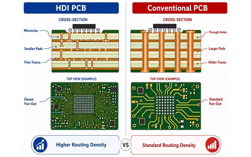
A standard multilayer PCB remains the better option when routing can be completed without microvias. HDI becomes worthwhile when through-hole pads block routing channels or force an unnecessary increase in board size or layer count.

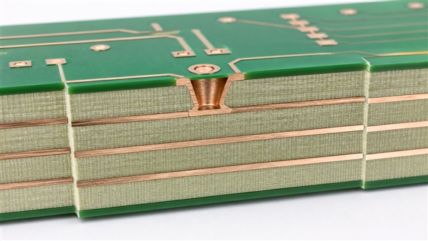
Comparison between HDI PCB and conventional multilayer PCB structures and BGA fan-out density

What Are the Main Types of HDI PCB Stackups?

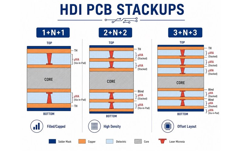
HDI stackups are commonly described as 1+N+1, 2+N+2, or 3+N+3. The outer numbers show the number of HDI build-up layers on each side. 鈥淣鈥?represents the central core structure.

HDI stackup Construction Typical use
1+N+1 One build-up layer on each side Moderate-density BGAs, industrial controls, and consumer products
2+N+2 Two build-up layers on each side Dense processors, communication modules, and medical electronics
3+N+3 Three build-up layers on each side Advanced computing and highly compact electronics
Any-layer HDI Microvias between many adjacent layers Highly miniaturized products and complex modules
Asymmetric HDI Different build-up structures on each side Boards with density concentrated on one surface

A 1+N+1 construction is usually the most economical HDI entry point. Moving to 2+N+2 or 3+N+3 should be driven by actual routing needs because every additional build-up level adds process steps and registration interfaces.

HDI PCB stackup comparison showing 1 plus N plus 1, 2 plus N plus 2, and 3 plus N plus 3 constructions

What Types of Vias Are Used in High-Density Interconnect PCBs?

An HDI board usually combines several via types rather than using microvias everywhere.

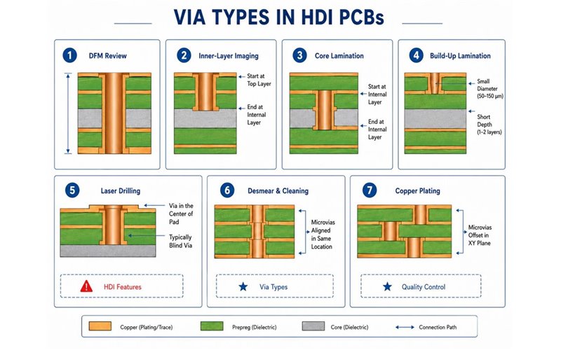
  • Plated through-hole: Connects the full board thickness and is often used for connectors, power, and component leads.
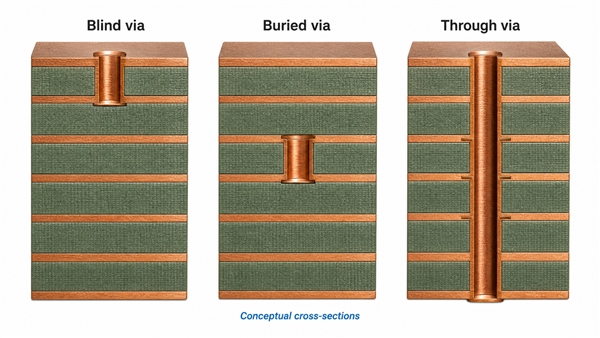
  • Blind via: Connects an outer layer to one or more inner layers without passing through the complete PCB.
  • Buried via: Connects internal layers and is not visible from the surface.
  • Laser microvia: A small blind via used for fine-pitch routing.
  • Via-in-pad microvia: Located directly inside a component pad, commonly beneath BGAs.
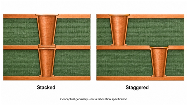
  • Staggered microvia: Microvias on adjacent levels are laterally offset.
  • Stacked microvia: Two or more microvias are aligned vertically.
  • Skip microvia: Connects non-adjacent layers through more than one dielectric layer.

Large mechanically drilled vias may still be better for high current, connector strength, and thermal transfer. The via architecture should follow the electrical and routing requirements, not a desire to use the most advanced-looking structure.

Cross-section illustrations of via structures used in high-density interconnect printed circuit boards

How Does the HDI PCB Manufacturing Process Work?

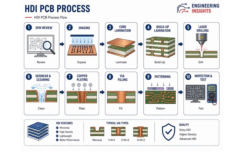
The exact HDI PCB manufacturing process depends on the stackup and microvia architecture. A typical route includes:

  1. DFM and stackup review: Confirm materials, dielectric thickness, microvia geometry, impedance, and copper weight.
  2. Inner-layer imaging and etching: Form and inspect the internal copper circuits.
  3. Buried-via processing: Drill, clean, plate, and inspect buried vias where required.
  4. Core lamination: Press the internal layers and prepreg into the central multilayer structure.
  5. Build-up lamination: Add thin dielectric and copper layers to the core.
  6. Laser drilling: Form controlled blind microvias.
  7. Desmear and cleaning: Remove laser residue and expose the target pads.
  8. Copper deposition and plating: Metallize the microvia walls and build the required copper thickness.
  9. Via filling and planarization: Fill via-in-pad and stacked microvias and level the surface.
  10. Repeated build-up processing: Repeat lamination, drilling, and plating for additional HDI levels.
  11. Final board processing: Complete through-holes, solder mask, surface finish, profiling, and legend.
  12. Inspection and test: Perform AOI, electrical testing, impedance testing, X-ray inspection, and microsection analysis as required.

The drill table, stackup, fabrication drawing, and layer files must show the same via start and stop layers. Conflicting data delays engineering review and can lead to an incorrect production route.

HDI PCB manufacturing process from DFM review and imaging to laser drilling, plating, via filling, patterning, and testing

Why Is Sequential Lamination Required in HDI PCB Fabrication?

Sequential lamination is required because each microvia level is built in stages. In a 2+N+2 structure, the core is produced first, followed by the first build-up layer and its microvias. A second dielectric is then laminated over that surface before the next microvia level is drilled.

When stacked microvias are used, the lower microvia usually needs to be filled and planarized before the next microvia is placed above it.

Each additional build-up level increases:

  • Lamination cycles
  • Laser drilling operations
  • Plating and filling work
  • Registration requirements
  • Thermal exposure
  • Inspection requirements
  • Manufacturing cost

This is why moving from 1+N+1 to 2+N+2 can affect cost and lead time more than simply adding two conventional copper layers.

What Materials Are Used for HDI PCB Manufacturing?

Material selection should consider lamination cycles, z-axis expansion, signal loss, assembly temperature, and long-term reliability.

Material type Suitable use Main consideration
Standard FR-4 Cost-sensitive, moderate-density HDI May be less suitable for repeated high-temperature processing
High-Tg FR-4 Industrial, automotive, and multilamination HDI Improved thermal and dimensional stability
Low-CTE laminate Reliability-sensitive microvia structures Reduces expansion stress during thermal cycling
Low-loss laminate High-speed communication and computing Higher material and processing cost
Resin-coated copper Thin build-up layers Suitable for laser microvia formation
Build-up film Very fine HDI structures Requires specialized production capability
Halogen-free laminate Products with environmental material requirements Thermal and drilling performance must still be checked

High-Tg FR-4 is suitable for many industrial HDI boards. A low-loss material is justified only when insertion loss, data rate, rise time, or signal-integrity targets require it.

Do not approve a laminate substitution based on Tg alone. Also compare Dk, Df, z-axis CTE, decomposition temperature, CAF resistance, moisture absorption, copper adhesion, glass style, and resin content.

HDI PCB Design Guidelines

  • Confirm the stackup before routing. Dielectric thickness affects microvia depth, impedance, board thickness, and lamination.
  • Use microvias only where density requires them. Standard vias can remain in open areas.
  • Keep the microvia aspect ratio low. A depth-to-diameter ratio around 0.6:1 to 0.8:1 provides a wider manufacturing window.
  • Use the largest practical microvia and pad. Smaller geometry increases registration and plating risk.
  • Fill and cap solderable via-in-pad structures. Open vias beneath BGA pads can draw solder away from the joint.
  • Limit stacked microvia levels. More stacked interfaces increase process complexity and thermal stress.
  • Balance copper across the board. Uneven copper can affect resin flow, bow, twist, and plating.
  • Use the production stackup for impedance calculations. Include actual dielectric thickness, copper thickness, copper profile, and solder mask.
  • Keep drill definitions consistent. Every via group needs clear start and stop layers.
  • Provide test coupons when needed. Impedance, registration, and microvia coupons support process verification.

A useful rule is to use the largest feature that still completes the routing. Reducing geometry simply because the CAD tool allows it reduces fabrication margin without necessarily improving the product.

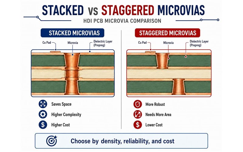
Stacked vs Staggered Microvias: Which Is Better?

Staggered microvias are usually preferred when enough lateral space is available. Stacked microvias are selected when routing density is more important than process simplicity.

Factor Staggered microvias Stacked microvias
Routing space Requires more lateral area Saves board area
Via filling Less demanding Lower vias normally need complete filling
Registration More forgiving Requires tighter vertical alignment
Process complexity Lower Higher
Cost Usually lower Usually higher
Reliability margin Generally wider More dependent on interface and plating quality
Best fit Industrial and reliability-sensitive products Dense BGA escape and compact electronics

Stacked microvias can be reliable when the lower vias are properly filled, planarized, aligned, and plated. For automotive, medical, aerospace, and long-life industrial products, staggered microvias are often the safer default unless layout density requires stacking.

Comparison of stacked and staggered microvias in an HDI PCB cross-section

What Common Defects Occur During HDI PCB Fabrication?

HDI defects are often internal, so visual inspection alone is not sufficient.

  • Microvia base separation: Weak connection between plated copper and the target pad.
  • Barrel or corner cracking: Related to thermal stress, copper ductility, or difficult geometry.
  • Plating voids: Incomplete copper coverage inside the microvia.
  • Incomplete via filling: Leaves a depression or internal void.
  • Excessive dimple: Creates an uneven via-in-pad surface.
  • Microvia misregistration: The drilled hole does not fully contact the target pad.
  • Resin voids or delamination: Caused by contamination, inadequate resin flow, or poor lamination control.
  • Fine-line opens or shorts: Linked to imaging, etching, or contamination issues.
  • CAF growth: Conductive paths develop through the laminate under moisture and electrical bias.
  • Bow and twist: Often related to asymmetric stackups or uneven copper distribution.

For reliability-sensitive boards, useful documentation can include microsection reports, impedance records, electrical test results, X-ray inspection, and thermal stress data.

What Factors Affect HDI PCB Fabrication Cost?

HDI cost is driven by process complexity, not only by layer count.

Cost factor Why it raises cost Practical control
Build-up levels More lamination and drilling cycles Use 1+N+1 where routing permits
Stacked microvias More filling, planarization, and alignment work Use staggered vias when space allows
Fine trace and space Reduces fabrication yield Restrict fine geometry to dense areas
Small microvias Tighter drilling and plating control Use larger geometry where possible
Via-in-pad quantity Adds filling and planarization Apply only where required
Specialized laminate Higher material cost and longer sourcing Use standard high-Tg FR-4 when suitable
Heavy copper Makes fine-line etching more difficult Separate high-current and fine-routing areas
Quick-turn schedule Requires priority engineering and processing Submit complete, approved files
Low quantity Setup cost is divided across fewer boards Use a production-compatible prototype design
Special testing Adds inspection and documentation Match testing to the end-use risk

Requesting a preliminary stackup before routing is one of the most effective cost controls. A well-planned 1+N+1 structure may replace a more expensive 2+N+2 design without affecting product performance.

Why Choose EBest Circuit for HDI PCB Fabrication?

HDI projects benefit from early communication between the customer and manufacturer. Stackup, microvia depth, filling method, material, impedance, and assembly requirements should be reviewed before final design release.

EBest Circuit, also known as Best Technology, supports HDI PCB fabrication from prototype review through PCB assembly and testing. Engineering discussions can cover:

  • 1+N+1 and 2+N+2 stackup planning
  • Laser microvia geometry
  • Stacked and staggered via selection
  • Via-in-pad filling and cap plating
  • High-Tg and low-loss materials
  • Controlled-impedance structures
  • Fine-pitch BGA fan-out
  • PCB assembly compatibility
  • DFM issues affecting yield, cost, or lead time

For an accurate quotation, provide:

  • Gerber, ODB++, or IPC-2581 data
  • NC drill files
  • Layer stackup
  • Fabrication drawing
  • Finished board thickness
  • Copper weight
  • Material requirement
  • Surface finish
  • Impedance table
  • Via-fill requirements
  • Order quantity
  • Testing requirements
  • Requested delivery date

FAQs

1. What does HDI mean in PCB fabrication?

HDI means high-density interconnect. It describes a PCB structure using microvias, thin dielectric layers, smaller pads, and fine routing to achieve higher wiring density.

2. What is the difference between HDI and multilayer PCB fabrication?

A conventional multilayer PCB mainly uses mechanically drilled through-holes. HDI fabrication adds laser microvias, sequential lamination, tighter registration, and often via filling.

3. What is a 1+N+1 HDI PCB?

It has one HDI build-up layer on each side of a central N-layer core. It is often the most cost-effective structure for moderate-density designs.

4. What is a 2+N+2 HDI PCB?

It has two HDI build-up layers on each side. It supports deeper microvia routing but requires more lamination and processing than 1+N+1.

5. Are HDI microvias always laser drilled?

Not by definition, but laser drilling is the standard production method because it creates small, controlled blind holes in thin dielectric layers.

6. What is the typical aspect ratio for a microvia?

A depth-to-diameter ratio of approximately 0.6:1 to 0.8:1 is commonly preferred. Ratios near 1:1 should be confirmed with the manufacturer.

7. Are stacked microvias reliable?

Yes, when they are properly filled, planarized, aligned, and plated. They still require tighter process control than staggered microvias.

8. Does via-in-pad need to be filled?

A via-in-pad beneath a soldered component pad should normally be filled and capped to prevent solder loss and provide a flat assembly surface.

9. How many lamination cycles does an HDI PCB require?

The number depends on the core, buried vias, and build-up levels. More complex structures require additional sequential lamination stages.

10. How long does quick-turn HDI PCB fabrication take?

Lead time depends on the stackup, material availability, via structure, quantity, and testing. A simple 1+N+1 prototype is normally faster than a stacked 2+N+2 or any-layer design.

11. What information should be included in an HDI fabrication drawing?

Include board dimensions, finished thickness, layer numbering, material, copper requirements, drill chart, via spans, filling requirements, surface finish, impedance values, tolerances, and inspection requirements.

12. How can engineers reduce HDI PCB manufacturing costs?

Use the simplest stackup that completes the routing. Prefer staggered microvias, standard materials, practical trace widths, and larger pads where possible. Limit via-in-pad and stacked structures to areas where they provide a measurable layout benefit.

Conclusion

HDI PCB fabrication is most valuable when fine-pitch components, limited board space, or dense routing make conventional through-hole construction impractical. The stackup, microvia structure, material, and lamination route should be settled before the layout is complete.

For an HDI stackup review, fabrication quotation, or PCB assembly discussion, contact EBest Circuit.

sales@bestpcbs.com


This HTML file is self-contained. All six illustrations are embedded in the file, and each figure includes an independent image download button.

You may also like

HDI PCB Fabrication Guide: Microvias, Stackups, DFM and Supplier Checks
Friday, July 10th, 2026

HDI PCB fabrication is the manufacturing process used to build high-density interconnect circuit boards with fine lines, laser microvias, blind vias, buried vias, via-in-pad structures, and sequential build-up layers. It is used when a conventional multilayer PCB cannot provide enough routing density, signal performance, or BGA escape space for compact electronics.

For engineers and sourcing teams, the right question is not only whether a factory can make an HDI PCB. The better question is whether the stackup, microvia structure, material choice, DFM review, inspection plan, and quotation data are mature enough for reliable production. EBest Circuit supports HDI PCB projects through PCB fabrication, DFM communication, prototype support, PCB assembly, component sourcing, and full turnkey manufacturing.

HDI PCB fabrication with fine traces, microvias and dense BGA routing areas
HDI PCB fabrication helps compact products use fine-line routing, microvias and dense layer transitions.

What Is HDI PCB Fabrication?

HDI PCB fabrication is a specialized PCB manufacturing flow for boards with higher wiring density than conventional through-hole multilayer PCBs. It usually combines fine copper patterning, laser drilling, blind and buried vias, sequential lamination, via plating, via filling, solder mask, surface finish, and electrical testing.

An HDI board may use blind microvias from an outer layer to an adjacent inner layer, buried vias between internal layers, or stacked and staggered microvias across build-up layers. These structures free routing channels under fine-pitch components and reduce the space consumed by large mechanical through-holes.

HDI fabrication is commonly used in communication modules, medical electronics, compact industrial controls, automotive electronics, cameras, wearable devices, IoT products, high-speed boards, and products using fine-pitch BGA or CSP packages.

When Is HDI Better Than a Standard Multilayer PCB?

HDI becomes useful when component density, routing escape, board size, or electrical performance makes a standard multilayer PCB inefficient. It should be chosen for a real design reason, not simply because it sounds more advanced.

Design situation Why HDI may help Engineering or sourcing note
Fine-pitch BGA or CSP packages Microvias can help escape dense component pins with less layer congestion. Confirm BGA pitch, via-in-pad rules, target pad size, and via filling early.
Very compact enclosure HDI can increase routing density without increasing board area. Compare HDI cost against a larger standard PCB before the mechanical design is frozen.
High-speed or RF routing Shorter transitions and controlled stackups can support cleaner signal paths. Ask for impedance stackup review and material confirmation before layout release.
High I/O count components Blind and buried vias create more routing channels under dense packages. Review drill maps, layer transitions, and lamination cycles with the fabricator.
Prototype routing failure HDI may solve routing blockage without adding many conventional layers. Use DFM review before assuming a more complex stackup is the only solution.

BestPCBs HDI PCB Fabrication Capability Snapshot

For a quotation-ready HDI project, capability should be discussed with the actual stackup, copper weight, material, panel size, quantity, and reliability target. The following values summarize useful starting points from EBest Circuit’s current PCB process capability data.

Capability area Available range or support Buyer note
Layer count Standard FR4: 1-10 layers; special multilayer FR4: 10-32 layers. Boards with 8 layers or more should use high-Tg material.
Laser blind / buried vias 0.10 mm laser blind/buried via capability. Useful for HDI build-up layers and fine-pitch component escape.
Finished hole diameter Standard minimum finished hole: 0.20 mm; special process: 0.15 mm. Mechanical blind/buried holes can also be reviewed down to 0.15 mm by special process.
Line width and spacing Standard 1 oz inner/outer layer: 4/4 mil; special process can review 3/3 mil for 1 oz and 1/2 oz cases. Heavy copper requires wider line and spacing rules.
Copper thickness Standard FR4 copper: 0.5 oz to 5 oz; special process: 5 oz to 20 oz. High-current HDI designs need early copper balance and plating review.
Surface finishes OSP, HASL, lead-free HASL, ENIG, immersion silver, immersion tin, ENEPIG, hard gold fingers, ENIG+OSP, and ENIG+hard gold fingers. Choose based on BGA assembly, shelf life, bonding, solderability, and contact wear.

These values are practical starting points, not a substitute for design review. A 3/3 mil line-space area, a 0.15 mm hole, or a 32-layer board should be checked against the actual copper weight, stackup, material, impedance requirement, and production quantity.

HDI Stackup Types and Via Structures

The HDI stackup defines how many build-up layers are added to the core and how microvias connect those layers. The choice affects routing density, lamination cycles, registration control, cost, and reliability.

Structure Typical use Manufacturing impact
1+N+1 HDI Moderate HDI density and fine-pitch component escape. Usually simpler and more economical than multi-step HDI build-up.
2+N+2 HDI Higher routing density and more complex BGA escape. Requires more sequential lamination control and tighter registration review.
Blind microvia Connects an outer layer to an adjacent inner layer. Usually laser drilled and plated; depth, diameter, and target pad must be reviewed.
Buried via Connects internal layers without reaching the outer layers. Requires internal drilling and plating before later lamination.
Stacked microvia Connects build-up layers vertically in the same position. Often requires copper filling and stronger reliability review.
Staggered microvia Offsets microvias between layers. Can reduce some stacked-via stress risk but uses more routing area.

EBest Circuit’s HDI product page discusses 1+N+1, 2+N+2, and every-layer interconnection structures. In a real project, the final structure should be selected by BGA pitch, I/O count, routing density, impedance needs, and reliability target.

HDI PCB Fabrication Process

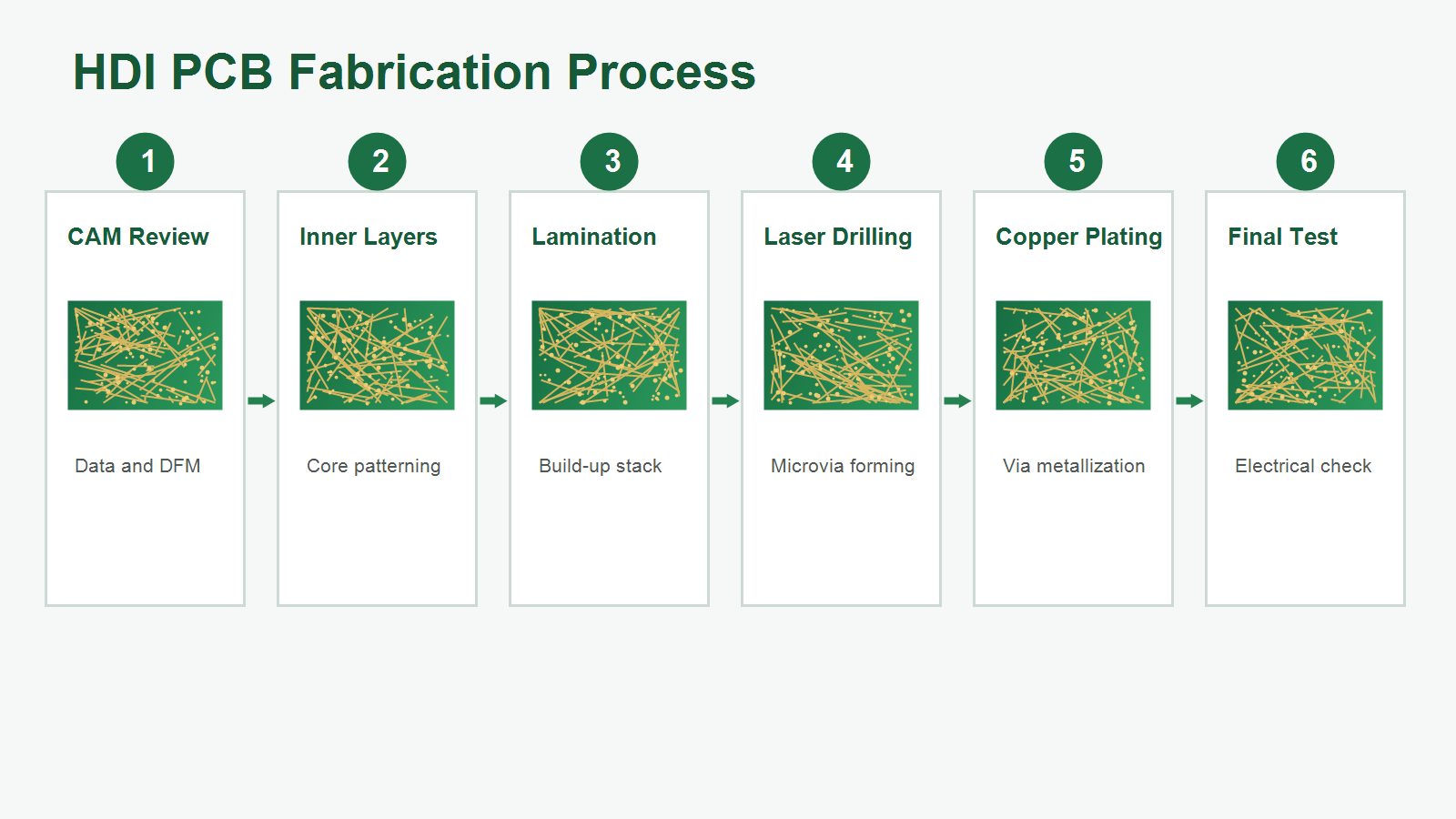
The HDI PCB fabrication process starts with engineering review and moves through inner-layer processing, lamination, laser drilling, copper plating, via filling, outer-layer patterning, solder mask, surface finish, and final testing.

HDI PCB fabrication process from CAM review to final electrical test
A practical HDI process flow includes DFM review, lamination, laser drilling, plating and final testing.
  1. CAM and DFM review: Check Gerber or ODB++ data, stackup, drill map, impedance notes, copper spacing, annular rings, via structures, and panelization.
  2. Inner-layer imaging and etching: Pattern internal copper layers and inspect them before they are buried inside the stack.
  3. Buried via processing: Drill, plate, and inspect internal vias where the HDI stackup requires them.
  4. Sequential lamination: Add build-up dielectric and copper layers in controlled lamination cycles.
  5. Laser drilling: Form microvias between adjacent layers for dense interconnect routing.
  6. Desmear and via preparation: Prepare the via surface for reliable copper deposition.
  7. Copper plating and via filling: Build conductive via walls and fill or cap vias when required by via-in-pad or stacked structures.
  8. Outer-layer imaging and etching: Define fine outer copper features and inspect for opens, shorts, and spacing issues.
  9. Solder mask and surface finish: Apply solder mask and finish pads with ENIG, ENEPIG, OSP, immersion silver, immersion tin, or another specified finish.
  10. Final inspection and test: Use AOI, electrical test, impedance test, microsection review, dimensional inspection, and final visual inspection where required.

Design Rules That Affect HDI Manufacturability

HDI manufacturability depends on whether the layout respects the fabricator’s real line width, spacing, pad, via, dielectric, copper, solder mask, and registration limits. Small design-rule changes can strongly affect yield, cost, and lead time.

  • Keep laser microvias within the manufacturer’s recommended diameter, depth, and layer-span limits.
  • Avoid stacked microvias unless routing density or electrical constraints truly require them.
  • Use via-in-pad only when it solves a fine-pitch component escape or assembly problem.
  • Confirm whether BGA pads require filled and capped vias to prevent solder wicking.
  • Use relaxed trace and space rules outside dense routing areas when possible.
  • Review copper balance to reduce lamination distortion and registration risk.
  • Define controlled impedance with stackup, tolerance, reference plane, and coupon requirements.
  • Send early BGA escape and placement data for DFM review before completing the full layout.

For dense products, the best workflow is collaborative. The PCB designer, fabricator, and assembler should review BGA escape, stackup, via filling, surface finish, and assembly process before the design is frozen.

Microvia Reliability Risks and How to Reduce Them

Microvia reliability depends on geometry, plating quality, via filling, material behavior, thermal stress, and the number of stacked levels. Common risks include voiding, weak target-pad connection, plating cracks, solder wicking, and registration misalignment.

Risk Possible cause Prevention or inspection point
Microvia voiding Incomplete filling or unstable plating control. Request microsection evidence and via fill confirmation.
Target pad separation Thermal stress or poor metallurgical connection at the via base. Review microvia geometry, material CTE, and thermal cycling requirements.
Stacked via fatigue Multiple stacked levels increasing local stress. Use staggered vias where possible or confirm copper-filled stacked via reliability.
Solder wicking in via-in-pad Unfilled or poorly capped via inside a component pad. Specify filled and capped via-in-pad for BGA pads when required.
Registration misalignment Sequential lamination movement and tight pad geometry. Use realistic capture pads and review layer-to-layer registration capability.

Materials and Surface Finishes for HDI Boards

HDI material and surface finish choices should match signal speed, thermal stress, soldering process, storage, reliability target, and cost. Standard FR4 may be suitable for many HDI boards, while high-speed, RF, high-temperature, or reliability-sensitive applications may need higher-performance laminates.

EBest Circuit’s material capability includes FR4 low-Tg, mid-Tg, high-Tg, halogen-free options, and special materials such as Isola, Rogers, Nelco, Taconic, PTFE, and other high-performance laminates when project requirements justify them. Surface finish options include OSP, HASL, lead-free HASL, ENIG, immersion silver, immersion tin, ENEPIG, hard gold fingers, ENIG+OSP, and ENIG+hard gold fingers.

Choice Where it matters Practical note
High-Tg FR4 Multilayer and reliability-sensitive HDI products. Use for 8-layer and above FR4 projects and applications with higher thermal stress.
Low-loss laminate High-speed, RF, antenna, and communication designs. Confirm Dk, Df, copper profile, impedance model, and availability before layout release.
Thin dielectric build-up layer Laser microvia formation and compact layer transitions. Microvia depth and target pad geometry must match the fabricator’s capability.
ENIG or ENEPIG BGA assembly, fine-pitch pads, contact reliability, and wire bonding in some designs. Choose based on assembly process, shelf life, bonding needs, and reliability requirement.
OSP, immersion silver, or immersion tin Cost-sensitive or process-specific applications. Review storage, handling, solderability, and assembly window with the assembler.

Quality Control and Testing for HDI PCB Fabrication

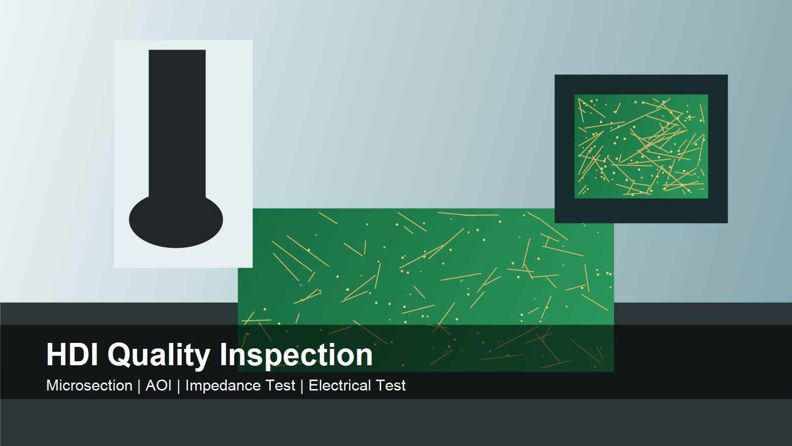
HDI quality control must verify both visible board quality and hidden interconnect reliability. Microvias and buried vias are not fully visible after lamination, so inspection must include structural evidence and process control, not only final appearance.

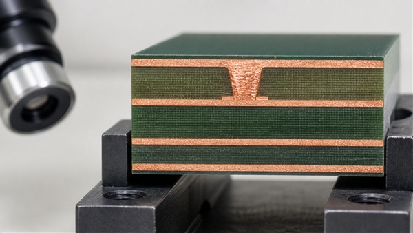
HDI PCB quality inspection using microsection, AOI, impedance and electrical test
HDI quality inspection should verify fine copper features, hidden vias, impedance and final electrical performance.
  • CAM and DFM review: catches manufacturability risk before production.
  • Inner-layer AOI: checks opens, shorts, over-etching, and spacing defects before lamination.
  • Laser via inspection: verifies microvia opening, position, and target pad relationship.
  • Microsection: verifies via wall quality, plating thickness, filling, target-pad connection, and lamination structure.
  • Impedance test: checks controlled impedance structures using coupons when specified.
  • Electrical test: confirms continuity and isolation before shipment or assembly.
  • Final visual and dimensional inspection: checks outline, solder mask, finish, legend, and workmanship.

HDI PCB Fabrication Cost Drivers

HDI PCB cost is driven by build-up complexity, lamination cycles, microvia structure, material choice, line and space requirements, via filling, surface finish, testing, and yield risk. A lower unit price is not always the lower project cost if it causes redesign, scrap, assembly defects, or reliability failure.

Cost driver Why it changes cost How to control it
Sequential lamination cycles More build-up cycles add process time, handling, registration risk, and cost. Use the simplest stackup that meets routing and reliability needs.
Stacked microvias They often need tighter process control and copper filling. Use staggered vias where layout allows.
Via-in-pad filling Filling, capping, and planarization add process steps. Apply via-in-pad only where it solves dense component escape or assembly needs.
Fine line and space Very fine copper features reduce process margin. Use 3/3 mil only where the dense area truly needs it.
Special laminates Low-loss or high-temperature materials increase material and handling cost. Match material to actual electrical and thermal requirements.
Testing requirements Impedance coupons, microsections, and reliability checks add time and evidence cost. Specify the tests needed for the application risk level.

What Files Are Needed for an HDI PCB Quote?

An accurate HDI PCB quote needs more than Gerber files. The supplier needs enough fabrication, stackup, material, via, finish, tolerance, and testing information to judge manufacturability and avoid hidden assumptions.

  • Gerber, ODB++, IPC-2581, or complete fabrication data.
  • NC drill files and drill map showing mechanical holes, blind vias, buried vias, and laser microvias.
  • Layer stackup with dielectric thickness, copper weight, material type, and controlled impedance notes.
  • Board outline, dimensions, tolerance, panelization, and routing notes.
  • Surface finish requirement, such as ENIG, ENEPIG, OSP, immersion silver, or immersion tin.
  • Via filling, capping, plugging, and via-in-pad requirements.
  • Solder mask color, legend color, UL or marking requirements if applicable.
  • Impedance control requirements and test coupon expectations.
  • IPC class, reliability, thermal cycling, automotive, medical, or compliance requirements if specified.
  • Quantity, prototype or mass production stage, delivery target, BOM, and assembly plan if PCBA is included.

How to Choose an HDI PCB Manufacturer

A capable HDI PCB manufacturer should explain the manufacturing trade-offs for your exact layout, not only list broad capability numbers. The supplier should review the stackup, microvia structure, material, via filling, inspection plan, and assembly needs before production.

Ask these questions before placing an HDI order:

  • Does the design fit standard FR4 production, or does it need special 10-32 layer review?
  • Can the laser blind/buried via structure use the 0.10 mm process safely with the selected dielectric?
  • Does the BGA escape require 3/3 mil special line/space or via-in-pad review?
  • Are filled and capped vias required under BGA pads?
  • What microsection evidence can be provided for first article approval?
  • How will impedance be calculated, built, and tested?
  • Which surface finish is recommended for the assembly process and shelf-life requirement?
  • Which requirements are standard process and which need special process review?

EBest Circuit supports HDI PCB projects with DFM communication, PCB fabrication, component sourcing, assembly, testing, and turnkey manufacturing. For HDI capability details, see the HDI PCB product page, the PCB capability page, and related PCB assembly services.

FAQ

What does HDI mean in PCB fabrication?

HDI means high-density interconnect. In PCB fabrication, it refers to boards built with denser routing features such as fine lines, smaller vias, blind vias, buried vias, and laser-drilled microvias.

Is HDI PCB fabrication the same as multilayer PCB fabrication?

No. HDI boards are multilayer boards, but they add specialized processes such as sequential lamination, laser drilling, microvia plating, and sometimes via filling and capping.

What is the minimum laser via size for BestPCBs HDI fabrication?

EBest Circuit’s current capability data lists 0.10 mm laser blind/buried via capability. The final approval depends on dielectric thickness, layer span, copper weight, pad geometry, and production quantity.

Can BestPCBs support 3/3 mil line width and spacing?

For 1 oz and 1/2 oz cases, special process review can reach 3/3 mil line width and spacing. Heavy copper designs require wider rules, so final approval should be checked with the stackup and copper thickness.

What is the difference between blind vias and buried vias?

A blind via connects an outer layer to an inner layer without passing through the whole board. A buried via connects only internal layers and is hidden after lamination.

Are stacked microvias reliable?

Stacked microvias can be reliable when the geometry, copper filling, plating process, material, and inspection controls are appropriate. For high-reliability products, review stacked versus staggered microvias during DFM.

Why is via-in-pad used in HDI PCB fabrication?

Via-in-pad is used when dense components, especially fine-pitch BGAs, do not leave enough room for traditional fanout routing. The via usually needs filling and capping to prevent solder wicking.

Which surface finish is best for HDI PCB fabrication?

There is no single best finish for every HDI board. ENIG is common for fine-pitch assembly, while ENEPIG, OSP, immersion silver, immersion tin, and hard gold options may fit different assembly and reliability needs.

Does HDI always reduce PCB cost?

No. HDI can reduce board size or layer count in some designs, but it also adds process cost. The total cost depends on whether the routing-density benefit offsets lamination, laser drilling, via filling, and inspection cost.

What is the biggest risk in HDI PCB fabrication?

The biggest risk is hidden interconnect reliability around microvias, plating, filling, and target-pad connection. DFM review, process control, microsection inspection, and realistic stackup choices reduce this risk.

Can HDI PCBs support high-speed signals?

Yes. HDI PCBs can support high-speed signals when the stackup, impedance control, material, return path, via structure, and fabrication tolerances are designed correctly.

What should I send for an HDI PCB quote?

Send Gerber or ODB++ files, drill files, stackup, material request, copper weight, impedance notes, via filling requirements, surface finish, quantity, delivery target, and assembly information if PCBA is included.

Final Takeaway

HDI PCB fabrication is valuable when compact size, fine-pitch components, high routing density, or signal requirements make standard multilayer routing inefficient. The best results come from early stackup planning, realistic microvia choices, material confirmation, DFM review, and supplier evidence rather than late-stage price shopping.

If you are evaluating an HDI PCB fabrication project, EBest Circuit can support PCB manufacturing, DFM review, component sourcing, assembly, testing, prototype builds, and production planning. Send your Gerber files, stackup, drill files, quantity, and assembly requirements to sales@bestpcbs.com for engineering review and quotation support.

You may also like

Can I design microvias in multilayer MCPCB?
Saturday, October 12th, 2024

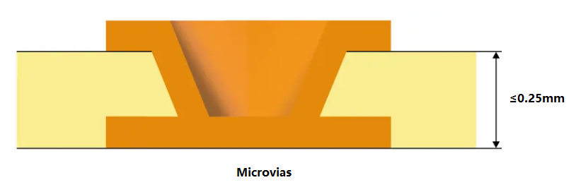
What is a Microvias?

A microvia is a small hole drilled into a PCB that connects different layers. They are essential for high-density interconnections and are commonly used in advanced electronic designs. Typically, microvias equal to or less than 150 microns drilled on the PCB board with a laser. In 2013, the IPC standard changed the definition of microvias to those with an aspect ratio of 1:1. Ratio of aperture to depth (not exceeding 0.25mm). Previously, micropores were less than or equal to 0.15 mm in diameter, so they typically spanned only one layer.

Can I design microvias in multilayer MCPCB?

Because the diameter is very small compared to mechanically drilled through holes (PTH), we define them as microvias, usually connecting only one layer of the board to its adjacent layers. These through holes reduce the possibility of any type of manufacturing defect because they are laser drilled, thus reducing the possibility of any residue remaining after the process. Because of their small size and ability to connect one layer to the next, they can make dense printed circuit boards with more complex designs.

Types of Microvias

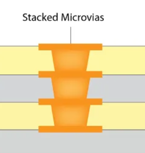
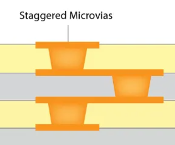
There are two types of microvias in the PCB design – stacked microvias and staggered microvias.

  • Stacked Microvias

Stacked microvias are formed by stacking multiple layers on top of each other to provide a path through which current flows. Create a hole in one layer and drill into another layer below. The top layer is welded or welded to the bottom layer to form an interconnect between the two layers. This allows for fast, efficient routing without compromising performance or reliability.

Can I design microvias in multilayer MCPCB?
  • Staggered Microvias

The interlaced microvias is aligned with the pad of the same layer, but is offset from its center by half of the pad diameter. The distance from its center to the edge of the board is also half the diameter of the pad. Staggered microvias allow you to place two through holes in a single pad without overlapping them or having to route wires on different layers together in this location. This type of microvias can be used for electrical connections to the surrounding brass pads and traces.

Can I design microvias in multilayer MCPCB?

What is the Difference Between Vias and Microvias?

Vias and microvias serve similar purposes in connecting different layers of a PCB, but they differ significantly in size and application.

1. Size

One of the most significant differences between vias and microvias is their size. Standard vias typically have a diameter greater than 150 micrometers (μm), while microvias are defined as having a diameter of 150 μm or less.

2. Design Complexity

As technology advances, the demand for higher circuit densities and more complex designs has grown. Microvias enable designers to create intricate multilayer circuits that were not possible with standard vias.

3. Layer Connection

Standard vias can connect any number of layers in a PCB, typically running from the outer layer through to the inner layers. In contrast, microvias are usually used for connecting one or two layers. Microvias are commonly employed in multilayer PCBs, where they can connect the outer layer to one or more inner layers without passing through the entire board.

4. Aspect Ratio

The aspect ratio, which is the ratio of the depth of a via to its diameter, is another important difference. Standard vias generally have lower aspect ratios, making them easier to fabricate. Microvias, due to their smaller size, often have higher aspect ratios. A typical aspect ratio for microvias ranges from 1:1 to 2:1.

5. Applications

Standard vias are commonly used in traditional PCB designs for applications where space is not as critical. They are suitable for general-purpose circuits, power distribution, and less complex layouts. In contrast, microvias are essential in high-density applications, such as smartphones, tablets, and advanced computing devices, where compact designs are necessary.

Microvias vs. Blind Via

Blind vias connect the outer layer of the PCB to one or more inner layers without penetrating the entire board. As the name suggests, these through-holes are “blind holes” because they are not visible from the other side of the PCB. Blind holes have several advantages, such as saving space on the board, enabling a more compact design, and improving signal integrity by reducing the length of the signal path.

The blind via passes through the surface layer of the PCB, extending through only a portion of the board to connect the surface layer to one or more inner layers. They are a key component in current PCB designs, allowing surface components to connect to inner layers while minimizing the number of layers required for wiring. The advantages of using blind vias including:

  • Increased density
  • Reduce the number of layers
  • Improved signal performance
  • Good for heat dissipation
  • Improve mechanical strength

Can Microvias be Designed in Multilayer MCPCB?

Yes, microvias can indeed be designed in multilayer MCPCBs. In fact, their small size and efficient design make them ideal for these types of boards. Multilayer MCPCBs often require compact interconnections to accommodate various functionalities, and microvias facilitate this need. By enabling multiple layers to connect efficiently, microvias enhance the overall performance of the MCPCB. Additionally, they contribute to improved thermal management, a critical factor in high-power applications. Their integration in multilayer designs is a significant advantage for modern electronics.

The process for using microvias in multilayer metal-based circuit boards includes the following key steps:

1. Inner laser drilling and plating: This is the first step in the production of microvias, precisely drilled by laser technology, and electroplated.

2. Resin filled: The micro-vias after electroplating are filled with resin to enhance the stability of the structure.

3. Resin grinding: Grind the orifice after the jack hole to ensure a smooth surface.

4. Electroplating: Metallize the surface of the orifice resin to achieve electrical interconnection between layers.

5. Inner circuit etching and outer layer lamination: To complete the production of the inner circuit, and the outer layer of laser drilling and graphic plating, and finally realize the production of multi-layer circuit board.

MCPCB Material in EBest Circuit (Best Technology)

Can I design microvias in multilayer MCPCB?

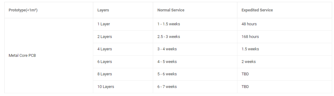
MCPCB Prototype Lead Time (Vary Depends on the MCPCB Design)

Can I design microvias in multilayer MCPCB?

You may also like