

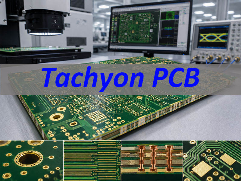
Tachyon PCB is a high-speed printed circuit board made with Tachyon 100G laminate and prepreg materials for advanced digital applications. It is important for 100G/400G communication systems, servers, switches, optical modules, and multilayer HDI boards where low signal loss, controlled impedance, accurate layer registration, and reliable assembly are required. This guide explains what Tachyon PCB is, why it is used for 20-layer HDI boards, what files are helpful for quotation, and what manufacturing capabilities customers should check before choosing a supplier.
EBest Circuit (Best Technology) supports high-speed PCB fabrication, multilayer HDI manufacturing, controlled impedance, DFM review, PCB layout manufacturability review, PCBA assembly, component sourcing, AOI, X-ray inspection, testing, and MES traceability. If you are preparing a Tachyon 100G HDI board for fabrication and assembly, you can send your available files to sales@bestpcbs.com for engineering review and quotation support.
What Is a Tachyon PCB?
A Tachyon PCB is normally a high-speed PCB manufactured with Tachyon 100G or related Tachyon laminate materials. It is used when a board needs stronger signal integrity than standard FR4 can usually support.
Key points:
- Material type: ultra-low-loss high-speed PCB laminate and prepreg
- Main purpose: support fast digital signal transmission
- Typical board type: multilayer PCB, HDI PCB, high-speed communication PCB
- Common applications: servers, switches, routers, optical communication modules, line cards, backplanes, data transmission boards
- Main concerns: insertion loss, impedance control, layer alignment, BGA breakout, via reliability, and assembly stability
For buyers, Tachyon PCB should be quoted as a high-performance engineering board, not as a standard multilayer PCB.
What Is Tachyon 100G PCB Material?
Tachyon 100G PCB material is used for very high-speed digital circuits. It helps reduce signal loss and supports more stable electrical performance in dense multilayer designs.
Important material features:
- Low Df: helps reduce dielectric loss
- Stable Dk: supports predictable impedance control
- High Tg: supports thermal reliability during PCB fabrication and SMT assembly
- Low Z-axis expansion: helps improve reliability in high-layer-count boards
- Smooth copper compatibility: helps reduce conductor loss
- Multilayer suitability: useful for dense signal, ground, and power layer structures
Typical Tachyon 100G projects may include:
- 16-layer, 20-layer, or higher multilayer PCBs
- HDI structures
- High-speed differential signals
- Fine-pitch BGA routing areas
- Controlled impedance
- Via-in-pad and plated via filling
The material should be reviewed together with stack-up, copper thickness, prepreg selection, impedance requirement, and assembly process.
Why Use Tachyon 100G for a 20-Layer Multilayer HDI PCB?
A 20-layer HDI PCB usually contains dense routing, multiple reference planes, blind vias, buried vias, laser vias, and fine-pitch components. Tachyon 100G is selected when signal loss and impedance stability are critical.
Main reasons:
- High-speed performance
- Supports fast differential signal channels
- Helps reduce signal attenuation
- Improves signal stability across complex routing paths
- Multilayer stack-up support
- Suitable for signal, ground, and power layer separation
- Helps maintain stable dielectric behavior
- Supports complex 20-layer structures
- HDI routing density
- Supports blind vias and buried vias
- Helps BGA breakout areas
- Saves routing space in compact layouts
- Controlled impedance
- Supports 50Ω single-ended impedance
- Supports 90Ω or 100Ω differential impedance
- Requires accurate stack-up and process control
- Assembly reliability
- Supports fine-pitch BGA assembly
- Requires board flatness control
- Needs stable surface finish and via-in-pad quality
EBest Circuit (Best Technology) reviews stack-up, impedance, HDI via structure, BGA areas, and assembly files before production to reduce manufacturing and assembly risk.
What Files Are Needed for a Tachyon PCB Manufacturing Quote?
For a Tachyon PCB quotation, customers do not need to prepare every file before making first contact. A basic file set is enough for an initial review, while more complete files help EBest Circuit (Best Technology) provide a more accurate price and DFM feedback.
For an initial quotation, these files are usually enough:
- Gerber files
- Drill files
- Layer count
- Board size
- Material requirement, such as Tachyon 100G
- Quantity
- PCB only or PCB assembly requirement
For a more accurate PCB fabrication quote, these files are helpful:
- Stack-up drawing
- Impedance table
- Fabrication drawing
- Copper thickness
- Finished board thickness
- Surface finish
- Blind/buried via details
- Via filling or plugging requirement
- Testing or report requirements
For PCBA quotation, please add these files if available:
- BOM
- Pick and place file
- Assembly drawing
- Component polarity notes
- Special assembly notes
- Functional test requirement, if any
Key reminder:
- You can send available files first. Missing information can be clarified during engineering review.
- Stack-up helps confirm impedance and board thickness.
- Drill files help evaluate HDI process difficulty.
- BOM helps estimate sourcing and assembly cost.
- Assembly drawings help avoid polarity and placement mistakes.
For a faster review, send your available project files to EBest Circuit (Best Technology) at sales@bestpcbs.com. The engineering team can advise what extra details are needed after checking the project.
What Are the Key Manufacturing Challenges of a Tachyon 100G HDI PCB?
A Tachyon 100G HDI PCB is challenging because it combines high-speed material, high layer count, fine routing, strict impedance, and advanced via structures.
Main manufacturing challenges:
- Material control
- Laminate and prepreg matching
- Moisture control
- Material traceability
- Pressing parameter control
- 20-layer lamination
- Layer registration
- Resin flow control
- Copper balance
- Board thickness control
- Warpage prevention
- HDI via process
- Laser drilling
- Blind vias
- Buried vias
- Via-in-pad
- Resin plugging
- Plated via filling
- Fine line control
- Etching tolerance
- Line width consistency
- Spacing control
- Copper thickness control
- Impedance control
- Dielectric thickness control
- Trace geometry control
- Reference plane consistency
- TDR impedance testing
- Inspection
- AOI
- Electrical test
- Impedance test
- X-ray inspection when required
- Microsection report when required
EBest Circuit (Best Technology) uses DFM review and PCB layout manufacturability review to identify possible production risks before fabrication.
What PCB Process Capabilities Does EBest Circuit (Best Technology) Offer for Tachyon PCB?
For Tachyon PCB projects, customers usually care about high-speed material support, multilayer fabrication, HDI vias, impedance control, fine routing, surface finish, and testing. These process points directly affect signal integrity, assembly yield, and production reliability.
| Process Item | Capability |
|---|---|
| Layer count | 1–50 layers |
| Suitable project type | 20-layer Tachyon 100G HDI PCB |
| Board thickness | 0.4–6.0 mm standard |
| Finished thickness tolerance | ±10% for boards above 1.0 mm |
| High-speed material | Low loss, ultra-low loss, Isola options |
| Inner copper for high-speed PCB | 0.5–1 oz standard |
| Outer copper for high-speed PCB | 0.5–2 oz standard |
| Inner line/space | 3/3 mil standard for 0.5 oz copper |
| Outer line/space | 3.5/4 mil standard for 1 oz copper |
| Laser via | 0.10 mm standard |
| HDI process | Blind via, buried via, via-in-pad |
| Via filling | Resin plugging, plated via filling |
| Impedance tolerance | ±10% for ≥50Ω |
| Surface finish | ENIG, ENEPIG, OSP, immersion silver, immersion tin |
| Testing | AOI, electrical test, impedance test, X-ray when required |
Why these capabilities matter for Tachyon PCB:
- 20-layer structures need stable lamination, registration, and thickness control.
- High-speed channels need stack-up review and impedance control before fabrication.
- Fine-pitch BGA areas need reliable laser vias, via-in-pad, and filled via processes.
- SMT assembly needs suitable surface finish, board flatness, and pad quality.
- Testing reports help customers confirm electrical quality before shipment.
EBest Circuit (Best Technology) reviews the stack-up, impedance table, drill files, via structure, BGA areas, and assembly requirements before production. This helps customers confirm whether the Tachyon PCB can be fabricated, assembled, tested, and delivered with stable quality.
How Is Tachyon PCB Assembly Handled for High-Speed Boards?
Tachyon PCB assembly requires close coordination between bare board fabrication and SMT assembly. BGA pads, via-in-pad, surface finish, board flatness, and panelization all affect final assembly quality.
Before SMT assembly:
- Review BOM
- Check component package and pitch
- Confirm BGA, LGA, WLCSP, or SiP requirements
- Review stencil and solder paste opening
- Confirm panelization and fiducials
- Check surface finish and board flatness
During SMT assembly:
- Solder paste printing
- SPI inspection when required
- Pick-and-place programming
- Reflow profile control
- Fine-pitch component placement
- BGA and LGA soldering control
After SMT assembly:
- AOI inspection
- X-ray inspection for BGA and hidden solder joints
- First article inspection
- Functional testing when test procedure is available
- Final visual inspection
EBest Circuit (Best Technology) supports SMT assembly for:
- Rigid PCB assembly
- Multilayer PCB assembly
- HDI PCB assembly
- High-Tg PCB assembly
- Heavy copper PCB assembly
- Aluminum PCB assembly
- Copper substrate PCB assembly
- Ceramic PCB assembly
- Rogers and high-frequency PCB assembly
- Rigid-flex PCB assembly
- Medical electronics PCBA
- Industrial control PCBA
- Automotive electronics PCBA
- Communication electronics PCBA
For Tachyon PCB projects, one-stop PCB fabrication and PCBA assembly help reduce communication gaps between PCB production, component sourcing, SMT assembly, inspection, and testing.
20-Layer Tachyon 100G HDI PCB Case Study by EBest Circuit (Best Technology)
This case shows how EBest Circuit (Best Technology) supported a 20-layer Tachyon 100G HDI PCB project from file review to fabrication and assembly. The customer provided the original layout files, while EBest Circuit (Best Technology) focused on DFM review, PCB manufacturing, SMT assembly, testing, and documentation.
Project Overview
- High-speed HDI PCB and PCBA project
- Tachyon 100G material
- 20-layer structure
- SMT assembly required
- Main focus: impedance control, HDI vias, BGA assembly, and traceability
Customer Requirements
- 20-layer Tachyon 100G HDI PCB fabrication
- Controlled impedance
- Blind and buried vias
- Via-in-pad with reliable filling process
- Fine-pitch BGA assembly
- AOI, electrical test, impedance test, and X-ray inspection
- COC and quality reports for shipment
EBest Circuit (Best Technology)’s Support
- Reviewed stack-up, drill files, impedance table, and fabrication notes
- Checked HDI via structure and BGA-related manufacturability
- Provided DFM and PCB layout manufacturability feedback
- Manufactured the PCB according to approved production files
- Completed SMT assembly and inspection
- Supported required testing and shipment documentation
Project Result
- DFM risks were checked before production
- Impedance and HDI process requirements were confirmed
- PCB fabrication and SMT assembly were coordinated in one workflow
- BGA solder joints were inspected by X-ray
- Finished boards passed required electrical and inspection checks
- Shipment documents were prepared according to project requirements
Case Board Specifications
| Item | Specification |
|---|---|
| PCB Type | High-Speed HDI PCB |
| Material | Tachyon 100G |
| Layer Count | 20 Layers |
| Finished Thickness | 2.4 mm ±10% |
| Copper Thickness | Inner 0.5 oz / Outer Finished 1 oz |
| Surface Finish | ENIG |
| Via Structure | Blind Vias, Buried Vias, Via-in-Pad |
| Via Process | Resin Plugging and Plated Via Filling |
| Impedance Control | 50Ω Single-Ended / 100Ω Differential, ±10% |
| Solder Mask / Silkscreen | Green Solder Mask / White Silkscreen |
| Assembly Requirement | SMT Assembly with Fine-Pitch BGA |
| Inspection | AOI, 100% Electrical Test, Impedance Test, X-Ray for BGA |
| Standard | IPC-6012 Class 2, RoHS, UL94V-0 |
| Reports | COC, Electrical Test Report, Impedance Test Report, Microsection Report When Required |
Why Choose EBest Circuit (Best Technology) for Tachyon PCB Manufacturing and Assembly?
Choosing a Tachyon PCB manufacturer is not only about finding a lower price. For a 20-layer high-speed HDI board, customers need engineering review, process control, assembly support, inspection, and reliable communication.
Why customers choose EBest Circuit (Best Technology):
- High-speed PCB experience
- High-speed material processing
- Stack-up review
- Controlled impedance support
- High-frequency and high-speed PCB manufacturing experience
- HDI and multilayer capability
- Multilayer PCB fabrication
- HDI process review
- Laser via support
- Via-in-pad process
- Resin plugging and plated via filling
- PCB and PCBA in one workflow
- PCB fabrication
- Component sourcing
- SMT assembly
- AOI inspection
- X-ray inspection
- Testing support
- Quality support
- ISO 9001
- ISO 13485
- IATF 16949
- AS9100D
- MES traceability
- Production documentation support
- Engineering communication
- DFM review before fabrication
- BOM review before sourcing
- Assembly process review
- Technical feedback before quotation
- Prototype to batch production support
If you are preparing a Tachyon 100G PCB project, send your Gerber files, stack-up, BOM, and assembly files to sales@bestpcbs.com for quotation and engineering review by EBest Circuit (Best Technology).
FAQs About Tachyon PCB
What is a Tachyon PCB?
A Tachyon PCB is a high-speed printed circuit board made with Tachyon laminate and prepreg materials. It is commonly used for high-speed digital signal transmission, multilayer HDI boards, and communication electronics.
Is Tachyon 100G the same as FR4?
No. Standard FR4 is used for general PCB applications. Tachyon 100G is a low-loss high-speed PCB material for more demanding signal integrity requirements.
Can Tachyon 100G be used for a 20-layer HDI PCB?
Yes. Tachyon 100G can be used for 20-layer HDI PCB designs. Stack-up, impedance, HDI via structure, lamination sequence, and assembly requirements should be reviewed before production.
What files are needed for a Tachyon PCB quote?
For an initial review, Gerber files, drill files, material requirement, layer count, board size, quantity, and assembly requirement are helpful. Stack-up, impedance table, BOM, and assembly files can be added for a more accurate quote.
Can Tachyon PCB support controlled impedance?
Yes. Controlled impedance is common in Tachyon PCB projects. The manufacturer needs target impedance, tolerance, layer information, trace width, spacing, and stack-up details.
Can Tachyon PCB be assembled with BGA components?
Yes. Tachyon PCB can be assembled with BGA components. X-ray inspection is recommended for BGA and other hidden solder joints.
What affects the cost of a Tachyon PCB?
Cost is affected by material grade, layer count, board size, HDI structure, blind and buried vias, via filling, impedance tolerance, copper thickness, surface finish, assembly complexity, testing, and quantity.
Does EBest Circuit (Best Technology) support Tachyon PCB fabrication and assembly?
Yes. EBest Circuit (Best Technology) supports high-speed PCB fabrication, HDI manufacturing, controlled impedance, DFM review, component sourcing, SMT assembly, AOI, X-ray inspection, testing, and traceability support.
How can I start a Tachyon PCB quotation?
Send your available files first. Gerber files, drill files, stack-up, impedance table, BOM, pick-and-place file, and assembly drawing can help EBest Circuit (Best Technology) provide a more accurate quotation. Contact sales@bestpcbs.com for review.
You may also like


Tags: HDI PCB, high-speed pcb, Tachyon PCB