PCB manufacturing PCB manufacturing
Home > Blog

PCB Design Guidelines

PCB Edge Clearance: Copper, Components, Routing, and V-Score
Saturday, September 5th, 2026
Engineers reviewing PCB board-edge clearance on a production panel
PCB edge clearance must match the actual outline, separation process, enclosure and assembly method.

PCB edge clearance is the controlled distance between the finished board outline and copper, traces, components, holes, slots or other functional features. It protects those features from routing tolerance, V-score intrusion, tab removal, depanelization stress, enclosure interference and handling damage.

There is no single safe distance for every board. The correct keepout depends on what is near the edge and how that edge will be manufactured. A routed contour, V-score line, mouse-bite tab, plated edge and card-edge connector each need different DFM logic.

What PCB Edge Clearance Actually Controls

An edge-clearance rule reserves manufacturing and assembly margin around the final board boundary. The CAD outline is nominal; the finished edge has routing, scoring or breakaway variation. Copper and components must remain functional at the worst allowed result.

Separate rules by feature class. Copper-to-edge protects conductors; component-to-edge protects packages and solder joints; hole-to-edge protects mechanical strength; tooling clearance protects assembly access.

Copper and Traces Near a Routed PCB Edge

Routing removes material with a rotating tool whose path and diameter create a finite manufacturing envelope. Copper placed too close can be exposed, smeared, burred or cut. Inner-layer copper also matters even when it is invisible from the surface.

  • Define the finished outline in one authoritative layer.
  • Check copper on every signal, plane and mechanical layer.
  • Include route tolerance and any bevel or chamfer.
  • Review corners and internal cutouts separately.
  • Flag intentional exposed copper rather than relying on proximity.

Component-to-Board-Edge Clearance

A component needs space for placement, soldering, inspection, handling and the final enclosure—not just a footprint that stays inside the outline. Tall parts, connectors, switches and overhanging packages deserve special checks.

Depanelization can flex the board beside an edge. Solder joints and brittle components placed in that stress zone may crack even if assembly initially passes. Consider package orientation, support tooling and the direction in which tabs or scored rails are separated.

Holes, Slots, and Connectors at the Edge

Mounting holes and slots need enough remaining material to carry their mechanical load. A nominal center distance is not enough; review finished hole/slot size, positional tolerance, edge-process tolerance and the mating hardware.

Edge connectors may intentionally approach or cross the outline. Their fingers, bevel, mask opening and mating envelope should be explicitly defined. Ordinary keepout rules should not silently modify an intentional card-edge feature.

Not sure which edge keepout applies to your panel?

Send the Gerber/ODB++, outline, panel method, component drawing and enclosure constraints. EBest Circuit can review routed, scored and tabbed edges before production.

Routing vs V-Score Edge Keepouts

Edge method Main risk Review focus
Routed contour Tool-path and profile tolerance Copper, holes, cutouts, corner radii
V-score Blade path, residual web and separation stress Components/copper on both board faces
Mouse-bite tab Breakout nibs and local bending Tab placement, perforations and nearby parts
Solid breakaway tab Manual/tool separation load Stress direction and finishing operation
Plated edge Intentional copper exposure/process continuity Layer connection, tabs and keepout exceptions

V-scoring normally follows straight lines and affects both faces. Routing supports complex contours but needs tool access and radius allowances. For a broader comparison, see V-grooves vs tab routing.

Do not measure every keepout from an idealized centerline. For routing, reference the finished profile and its allowed tolerance. For scoring, account for the actual cut path and residual web. At mixed edges, divide the outline into process zones so the CAD rules reflect the local separation method rather than applying one global value.

Mouse Bites, Breakaway Tabs, and Depanelization Stress

Tabs are temporary panel structures, but their removal can permanently damage nearby circuitry. Keep fragile components, small solder joints, ceramic packages and critical traces away from high-strain locations when possible.

Mouse-bite perforations leave small edge remnants that may require finishing. Tab position must also allow depaneling tools and avoid blocking connectors or enclosure surfaces. Review the separated board, not only the intact panel.
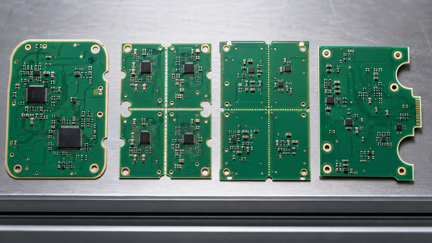
PCB examples with routed scored tabbed and shaped board edges
Edge-processing method changes the mechanical and copper keepout needed around the finished board.

Edge Plating and Card Fingers Are Intentional Exceptions

Edge plating deliberately brings copper to the finished contour, so standard copper keepouts cannot be applied blindly. The fabrication data should define which layers connect, where plating starts/stops and how panel tabs avoid interrupting the plated region.

Review grounding, shielding and connector intent as well as manufacturability. Our PCB edge-plating design guide covers the handoff in detail.

High Voltage and Harsh-Environment Edge Clearance

Electrical clearance to a board edge can be more demanding than basic routing capability. Pollution, moisture, coating strategy, altitude, contamination and enclosure geometry can affect creepage and clearance decisions.

Do not use a generic fabrication keepout as proof of electrical safety. Identify the working voltage, environment, insulation concept and applicable product requirements, then coordinate layout and manufacturing rules.

Assembly Tooling, Conveyors, and Test Access

Assembly may need edge rails, clamps, conveyor contact, selective-solder fixtures or depaneling support. Components or solder joints inside those zones can collide with tooling or prevent stable support.

Share the panel and assembly concept early. A bare-board outline may be manufacturable while the assembled panel is impossible to transport or fixture. Test points and programming connectors near an edge also need probe and cable access.

Board Outline Data and DFM Communication

A clean, closed and uniquely identified outline prevents many edge-clearance errors. Remove duplicate contours, ambiguous construction lines and conflicting dimensions. Define internal cutouts, slots, radii, bevels and controlled edge features.

The panel drawing should show rails, tabs, scores, tooling holes, fiducials and separation notes. If the fabricator may change tab positions, define which component/copper zones are protected and require approval for functional changes.

Compare the bare-board outline with the mechanical enclosure model and the assembled-component body outlines. A connector can satisfy copper keepout while its housing, latch or cable still collides with the case. Likewise, a mounting boss or gasket can overlap a component courtyard even when the PCB profile itself is correct.

Need routing, scoring, and assembly rules reviewed together?

Provide the board outline, panel drawing, BOM/CPL, enclosure and separation method. We can flag conflicts before tooling is released.

PCB Edge-Clearance Checklist Before Release

  1. Confirm the authoritative finished-board outline.
  2. Identify routing, scoring, tabs and intentional plated edges.
  3. Check copper and planes on every layer.
  4. Review components by body, courtyard and assembly access.
  5. Check holes/slots against finished geometry and loads.
  6. Protect brittle parts from depanelization stress.
  7. Include enclosure, connector and keepout envelopes.
  8. Separate electrical-safety spacing from fabrication capability.
  9. Review the assembled and separated board.
  10. Freeze the approved panel revision and deviation process.

What to Send for EBest Circuit Review and Quotation

Send Gerber or ODB++, drill/rout data, fabrication and panel drawings, stackup, BOM, CPL, enclosure constraints, edge-connector details, quantities, assembly requirements, test needs and target delivery.

EBest Circuit can review file consistency and edge-process conflicts before quotation. Specific clearance capability must be confirmed against the selected construction, panel method and approved production route.

PCB Edge Clearance FAQ

What is PCB edge clearance?

It is the reserved distance between the finished board boundary and functional copper, components, holes or other features.

Is component clearance the same as copper clearance?

No. Components add assembly, tooling, enclosure and stress considerations beyond copper fabrication risk.

Does V-scoring need more keepout than routing?

It often needs a different keepout because blade travel and separation stress affect both faces; use the supplier’s process-specific rule.

Can copper touch the PCB edge?

Only when intentionally designed and approved, such as edge plating or card fingers.

Why keep ceramic components away from breakaway tabs?

Local bending during separation can stress brittle bodies and solder joints.

Do internal-layer planes need edge checks?

Yes. Hidden copper can be exposed by routing or violate electrical/mechanical requirements.

How should mounting holes near an edge be reviewed?

Use finished hole size, position, remaining material, load and mating hardware—not center distance alone.

Does the enclosure define component-to-edge clearance?

It contributes a mechanical envelope, but manufacturing and assembly access must also be satisfied.

What outline errors commonly cause problems?

Duplicate/open contours, conflicting layers, missing cutouts and ambiguous score or route lines.

What files are needed for edge-clearance DFM?

Provide board/panel data, outline and rout files, BOM/CPL, enclosure and connector information, quantities and assembly method.

Protect the edge before panelization turns it into a production constraint.

Send your PCB files, panel method, component data and target delivery.

You may also like

PCB Hole Size Tolerance: PTH, NPTH, and Press-Fit Guide
Saturday, September 5th, 2026
PCB quality engineer measuring finished hole size with optical equipment and pin gauges
Finished-hole tolerance must match the hole function, plating condition and agreed measurement method.

PCB hole size tolerance defines the acceptable range of the finished hole, not simply the diameter of the drill tool. Plated through holes (PTH), non-plated holes (NPTH), vias and press-fit holes serve different functions, so one blanket tolerance rarely produces the best balance of fit, reliability, yield and cost.

The drawing should state whether each dimension is finished or drilled, whether plating is present, what feature mates with the hole, and how acceptance will be measured. Without those details, a supplier may meet a numerical callout while missing the assembly requirement.

What PCB Hole Size Tolerance Actually Controls

A tolerance controls the allowed upper and lower finished diameter for a defined hole class. It protects lead insertion, fastener fit, press-fit retention, plating reliability or via geometry. The tolerance should be derived from that function.

A nominal value alone is incomplete. A drawing needs a plus/minus or limit range, the plated status and any positional or geometric requirement that affects fit.

Drill Tool Size vs Finished Hole Size

Mechanical drill diameter is a manufacturing input; finished hole diameter is the inspected output. For a PTH, copper deposition reduces the open diameter after drilling. Cleaning, desmear, plating distribution and measurement method affect the final result.

NPTH features normally do not receive barrel copper, but routing/drilling variation, material behavior and finishing still matter. Do not copy a finished size into the drill file and assume the fabricator will interpret the required allowance.

How PTH and NPTH Hole Tolerances Differ

Hole class Primary function Tolerance evidence
PTH component hole Lead insertion plus reliable plated connection Finished diameter, plating and lead envelope
Via Electrical interconnection Finished hole, aspect ratio, annular ring and plating
NPTH mounting hole Mechanical clearance or location Finished diameter, position and mating hardware
Press-fit hole Controlled interference with compliant pin Connector specification, finished diameter and plating
Slot Tab, lead or mechanical feature Finished width/length, radii and plated status

Keep PTH and NPTH features separate in the drill data and drawing. Ambiguous mixed tables are a common source of quoting and production errors.

Why Press-Fit Holes Need a Functional Window

Press-fit performance depends on the relationship between the finished plated hole and the connector pin system. A hole that is too small may raise insertion force or damage the barrel; one that is too large may reduce retention or electrical contact.

Use the connector manufacturer’s approved finished-hole window and identify the pin part number. Align it with plating, board thickness, copper construction, insertion tooling and inspection. Our press-fit PCB assembly guide explains the broader process.

Need a hole table checked before PCB release?

Send the drill files, fabrication drawing, connector data, stackup and finished-hole requirements. EBest Circuit can flag ambiguous plated status and tolerance conflicts.

How Via Tolerance Interacts with Annular Ring

Finished-hole variation and positional variation both consume the copper land around a via. A larger finished diameter can reduce remaining annular ring even when the hole center is unchanged; registration shift can reduce it on one side.

Review pad diameter, finished hole, plating allowance, layer registration and breakout criteria together. See the annular ring guide and PCB aspect-ratio guide.

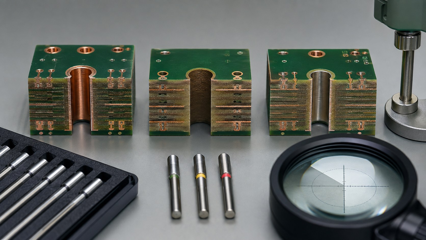
Cross-section samples comparing plated non-plated and press-fit PCB holes
PTH, NPTH and press-fit holes need different acceptance logic even when nominal diameters look similar.

Manufacturing Variables Behind Finished-Hole Variation

Finished size is influenced by more than tool diameter. Drill wear, runout, panel-stack setup, laminate movement, desmear, electroless copper, electrolytic plating and local current distribution can change the result.

  • Tool selection and wear influence the drilled opening.
  • Material and stack height affect drilling behavior.
  • Cleaning/desmear prepares the wall before metallization.
  • Barrel copper reduces the open diameter of plated holes.
  • Plating distribution can vary across a panel.
  • Final finish or secondary operations may alter particular features.

These variables explain why capability must be confirmed for the actual stackup and hole class, not copied from a generic tolerance table.

How Finished PCB Hole Size Is Measured

The measurement method must suit the hole and acceptance purpose. Pin gauges can quickly verify functional pass/fail windows; optical systems can measure diameter and location; cross-sections can show plating and wall condition.

Agree whether the reported result is a minimum diameter, maximum diameter, two-axis optical value or gauge acceptance. Sampling location and lot coverage also matter when plating varies across the panel.

Diameter tolerance must also be separated from positional tolerance. A hole can have the correct opening but sit too far from its datum, pad or mating feature. Conversely, a correctly located center can still fail a functional gauge because the finished opening is undersize. For slots, measure width, end radii, length and position according to the drawing rather than reducing the feature to one diameter.

Measurement timing should be clear. A result taken before plating does not prove the final PTH opening, while an inspection after an unapproved secondary operation may no longer represent the released process. Keep equipment calibration, sample identity and revision traceable to the production lot.

Why Over-Tight Tolerances Increase Cost and Risk

A tolerance tighter than the product needs can force special tooling, sorting, additional coupons, lower panel utilization or extra process controls. It may also reduce supplier options without improving assembly.

Classify holes by function. Apply tight limits only to features that require them, such as qualified press-fit systems or precision mechanical interfaces. Use the fabricator’s standard capability where it satisfies ordinary via or lead-clearance needs.

How to Build a Clear Hole and Slot Table

  1. Assign a unique class to each functional hole family.
  2. State PTH, NPTH or other required treatment.
  3. Specify finished size and tolerance or limit range.
  4. Identify quantity and associated drill-tool reference.
  5. Separate round holes from plated/non-plated slots.
  6. Call out press-fit part numbers and approved windows.
  7. State positional requirements where mechanical fit depends on them.
  8. Keep Gerber/ODB++, NC drill and drawing revisions synchronized.

For base size selection, review the protected standard PCB drill sizes guide.

Supplier Evidence and Nonconformance Review

Acceptance evidence should prove the required finished condition. Depending on risk, that can include first-piece measurements, gauge results, cross-sections, plating records, coordinate reports and lot traceability.

If a hole is out of tolerance, determine scope and function before disposition. Do not enlarge, replate or accept a critical feature without confirming its effect on annular ring, barrel copper, fit and reliability.

Comparing two PCB quotes with different hole assumptions?

Send both interpretations with the board files and mating-part data. We can help normalize finished-size, plating and inspection requirements.

PCB Hole Tolerance Decision Checklist

  • Is the value a drill size or finished size?
  • Is the feature plated, non-plated or press-fit?
  • What part, lead, pin or fastener must fit?
  • Does annular ring remain acceptable at worst case?
  • Are position and diameter tolerances separated?
  • Is the measurement method defined?
  • Are only functional holes tightly controlled?
  • Do all released files use the same revision?

What to Send for EBest Circuit Review and Quotation

Send Gerber or ODB++, NC drill data, fabrication drawing, stackup, materials, copper requirements, hole/slot table, connector or hardware specifications, quantities, assembly needs, inspection level and target delivery.
EBest Circuit can review data consistency and return questions before quotation. Specific tolerance capability must be confirmed against the selected construction and approved manufacturing route.

PCB Hole Size Tolerance FAQ

What is PCB hole size tolerance?

It is the allowed range around a defined finished or drilled hole dimension.

Is drill size the same as finished hole size?

No. Plating and other processing change the final opening, especially for PTH features.

Do PTH and NPTH holes use the same tolerance?

Not automatically. Their processes and functions differ, so they should be specified separately.

Why are press-fit holes more sensitive?

The finished plated diameter directly affects insertion force, retention and contact behavior.

How is a finished hole measured?

Common methods include calibrated pin gauges, optical measurement and cross-section analysis.

Does plating reduce hole diameter?

Yes. Barrel copper occupies part of the drilled opening, so fabrication compensates from the finished requirement.

Can a larger hole reduce annular ring?

Yes. Increasing the opening leaves less copper land around the hole.

Should every hole receive a tight tolerance?

No. Tighten only features whose fit or reliability requires it.

What causes hole-size variation?

Tool condition, drilling setup, material behavior, cleaning, plating and measurement all contribute.

What files prevent tolerance mistakes?

Provide synchronized artwork, NC drill files, a finished-hole table, stackup and mating-part specifications.

Make every critical hole measurable and manufacturable.

Send your PCB files, hole table, connector data, quantities and target delivery.

You may also like

Stacked vs Staggered Microvias: Reliability and HDI DFM
Saturday, September 5th, 2026
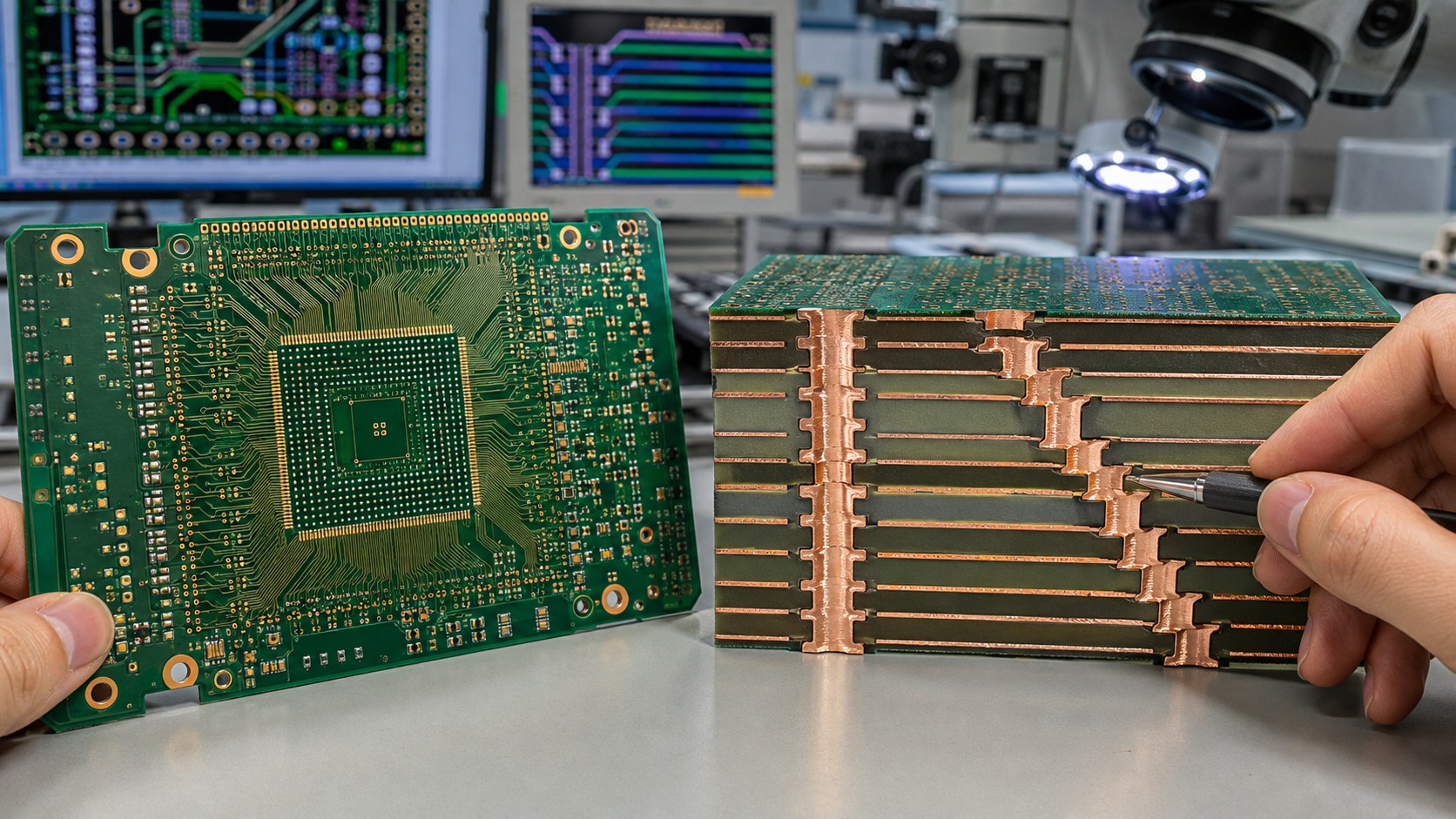
HDI PCB and cross-section comparing stacked and staggered microvia structures
Stacked and staggered microvias solve different HDI routing problems and create different fabrication controls.

Stacked microvias align vertically through successive build-up layers, while staggered microvias step sideways from one layer transition to the next. Stacking preserves routing area and can support dense BGA escape, but it concentrates manufacturing interfaces in one column. Staggering needs more lateral space, yet it can simplify filling and reduce dependence on a long, perfectly aligned vertical structure.

The choice is not “advanced versus basic.” It should be made from the actual layer transitions, package pitch, routing channels, dielectric thickness, via geometry, assembly profile and the fabricator’s qualified HDI process.

Stacked vs Staggered Microvias at a Glance

Decision factor Stacked microvias Staggered microvias
Routing area Small vertical footprint Needs lateral offset and landing space
Build dependency Relies on aligned, filled underlying structures Each transition lands on an offset capture pad
Process sensitivity Higher sensitivity to fill, planarity and registration More layout area but fewer vertical interfaces in one column
Typical reason to choose Very dense escape or constrained routing corridor Available area and preference for a less concentrated structure
DFM evidence Stackup, fill plan, cross-sections and qualification data Offset geometry, capture pads, registration and layer-clearance review

This comparison is directional. Final geometry and permitted layer combinations must come from the selected manufacturer’s capability review, not from a universal online rule.

How Stacked and Staggered Microvia Structures Are Built

Both structures are created through sequential build-up: form one dielectric layer, laser-drill the microvia, metallize it, then repeat for the next layer transition. A stacked design places the next microvia directly over the filled and planarized structure below. A staggered design shifts the next via so it lands on a separate capture pad.

That sequence makes stackup communication essential. A drawing that only says “blind via” does not tell CAM which layers connect, whether vias stack, whether fill is required, or which structures carry critical signals.

Why Stacked Microvias Save Routing Area

A vertical stack uses less planar space than an offset chain. This can preserve escape channels under fine-pitch BGAs, shorten transitions and keep nearby routing available for power, ground or high-speed nets.

The density benefit is real only if the structure can be manufactured reliably. Adding more transitions to a column increases dependency on each laser-drill, metallization, fill, planarization and registration step. Designers should not stack automatically where a staggered route, buried via or different fanout could meet the same electrical task.

Why Staggered Microvias Can Simplify Reliability Control

Staggering distributes adjacent microvias laterally instead of building one continuous vertical column. When the package and routing area allow the offsets, it can reduce reliance on the surface of a filled microvia as the foundation for the next laser via.

The tradeoff is space. Every offset needs a valid capture pad, trace connection and clearance from adjacent features. A loose stagger can also make the route longer or consume a channel needed by another net.

Unsure whether your HDI transition should stack or stagger?

Send the BGA map, stackup, via table, critical nets and available escape geometry. EBest Circuit can review the structure before artwork release.

Reliability Risks That Need Attention in Stacked Structures

The most important risk is an imperfect interface inside a structure that depends on every layer transition. Incomplete copper fill, voids, depressed fill, weak interconnection, misregistration or material stress can accumulate through the column.

  • A void or fill depression can affect the landing surface for the next microvia.
  • Registration error can reduce the effective capture area at an interface.
  • Repeated thermal excursions can stress copper-to-copper and copper-to-dielectric interfaces.
  • Material expansion behavior influences strain during reflow and service.
  • A structure that passes continuity may still require cross-sectional or reliability evidence.

Reliability cannot be inferred from the word “filled.” The specification should identify the stack, materials, acceptance criteria and required qualification evidence.

Capture Pads, Alignment, and Registration

Capture-pad geometry must tolerate the combined registration budget of imaging, lamination and laser drilling. A nominally centered CAD feature can lose effective land if process shifts align in the same direction.

For stacked vias, alignment must support the interface between successive features. For staggered vias, the offset must leave enough pad and connecting copper without violating spacing or blocking escape routes. Review finished geometry rather than judging only the drill file.

Related design foundations are covered in our PCB annular ring guide and microvia aspect-ratio guide.

Cross-sectional comparison of vertical stacked microvias and offset staggered microvias
A stacked column depends on aligned filled interfaces; a staggered chain trades lateral area for separated layer transitions.

Why Copper Filling and Planarization Matter

A microvia that supports another microvia generally needs a controlled filled and planarized surface. The next build-up layer must start from a stable landing condition. Fill voids, overfill, underfill or an uneven surface can affect imaging, lamination and the next laser-drilled feature.

Specify the required structure and acceptance result, then let the fabricator propose the qualified fill route. Do not substitute generic material names or assumed plating values for process evidence. Via-in-pad applications add assembly-flatness and solder-control concerns; see the VIPPO design and inspection guide.

Signal, Power, and Thermal Considerations

Geometry selection must serve the net, not only fabrication convenience. A compact stacked transition may reduce routing detour, but the complete return path, reference-plane change, anti-pad and nearby stitching strategy still determine electrical behavior.

For power paths, review current distribution and copper connection at every layer. Do not describe a microvia stack as a thermal solution without checking the complete heat path. Multiple distributed structures may behave differently from one concentrated column.

Cost and Lead-Time Drivers

Cost follows sequential build complexity, yield exposure, fill requirements, registration demands, inspection and qualification—not the via name alone. A dense stacked design may require more controlled cycles and evidence, while staggering may require a larger breakout region or another routing layer.

Ask for alternatives during DFM. A small fanout change, adjusted layer transition or mixed structure can reduce risk without changing the product function. Compare proposals using the same stackup and acceptance requirements.

Need a manufacturable microvia cost comparison?

Provide the current and acceptable alternative stackups, quantities, material needs, BGA pitch and inspection level. We can compare the real process impact.

Inspection and Qualification Evidence to Request

Use evidence that represents the actual microvia structure and production process. Useful controls can include coupon design, cross-sections, plating/fill review, registration checks, electrical test and agreed thermal-stress or reliability qualification.

The inspection plan should identify which stack is sampled, where coupons are placed, how interfaces are judged and what happens after a nonconformance. A generic statement that the board is electrically tested does not replace structural evidence.

Decision Checklist: Stack, Stagger, or Redesign the Transition

  1. Map every required layer transition from the actual net and BGA escape.
  2. Confirm how much lateral routing area is available.
  3. Identify which structures must align vertically and why.
  4. Review microvia geometry against each dielectric layer.
  5. Confirm capture pads, clearances, fill and planarization.
  6. Ask for the fabricator’s qualified structure and inspection evidence.
  7. Compare a staggered or mixed alternative before locking a tall stack.
  8. Freeze the approved via table, stackup and deviation process.

What to Send for EBest Circuit HDI DFM and Quotation

A useful RFQ connects design files to the exact microvia structure. Send Gerber or ODB++, drill/via data, fabrication drawing, stackup, material requirements, BGA package information, critical nets, controlled-impedance targets, quantities, assembly needs, inspection requirements and target delivery.

EBest Circuit can review whether the proposed stack, stagger or mixed strategy is clear and suitable for quotation, flag missing information and return project-specific questions. Any dimensional or process capability must be confirmed against the current build and approved factory route.

Stacked vs Staggered Microvia FAQ

What is the main difference between stacked and staggered microvias?

Stacked microvias align vertically; staggered microvias shift laterally between successive layer transitions.

Are staggered microvias always more reliable?

No. They can avoid a continuous vertical interface column, but reliability still depends on geometry, materials, process control and the actual design.

Why use stacked microvias?

They preserve routing area and can enable dense vertical transitions where the BGA escape or board outline leaves little lateral space.

Do stacked microvias need copper filling?

A microvia used as the landing foundation for another typically needs a qualified fill and planarization process. Confirm the exact structure with the fabricator.

How many microvias can be stacked?

There is no responsible universal answer. The permitted structure depends on the selected manufacturer’s qualified process, materials, dimensions and reliability requirements.

What is a microvia capture pad?

It is the copper land where the laser-drilled microvia terminates and connects to the target layer.

Can stacked and staggered microvias be mixed?

Yes, a board may use different structures where density and risk differ, provided the via table and stackup define them clearly.

Does electrical test prove a microvia stack is structurally reliable?

Electrical test confirms connectivity at test time; structural and reliability evidence may still be required for critical builds.

What data prevents microvia quotation errors?

Provide layer-pair definitions, stackup, hole/pad data, fill needs, quantities, materials, inspection criteria and any approved alternatives.

When should the fabricator review the microvia strategy?

Before layout constraints are frozen, and again before production release after the complete stackup and files are available.

Validate the HDI via structure before it becomes a yield problem.

Send your Gerber/ODB++, drill data, stackup, BGA map, materials, quantities and target delivery.

You may also like

PCB Etch Compensation: Trace Width, CAM Data, and DFM
Saturday, September 5th, 2026
CAM engineer reviewing PCB etch compensation beside a precision copper etching line
Etch compensation is a controlled CAM adjustment used to deliver the intended finished copper geometry after imaging and etching.

PCB etch compensation is the controlled enlargement or adjustment of production artwork so the finished copper feature lands near the released design target after etching. Because etchant removes copper vertically and laterally, the copper remaining on the panel will not exactly match an uncompensated image.

Designers should normally release nominal functional geometry and fabrication requirements—not guess a universal offset. The fabricator applies process-specific CAM compensation using the actual copper thickness, layer type, feature density, imaging route and qualified etch data. DFM review should make ownership and any design-impacting change explicit.

What PCB Etch Compensation Changes

Compensation changes the production image used to form traces, spaces, pads and other copper features before etching. It does not change the electrical design intent. A trace may be imaged wider so lateral copper loss produces the target finished width; isolated or dense features may require different treatment.

CAM software can apply rules by layer, feature class, orientation or local density. Those rules belong to the fabricator’s controlled process. They should not be confused with arbitrary global scaling or an undocumented change to the customer data.

Why Nominal Artwork Does Not Equal Finished Copper Geometry

Wet etching attacks exposed copper from the top and from the sides. The resist protects the intended image, but chemical access at the sidewall creates undercut. Copper thickness, etchant condition, transport, spray pattern, panel loading and dwell all influence the result.

The finished trace can therefore be narrower at one height than another. Inspection method matters: a top-view measurement, base-width measurement and cross-sectional measurement do not describe exactly the same geometry. Drawings and reports should identify the measurement basis.

For the broader manufacturing sequence, see PCB etching process and quality control.

Etch Factor, Undercut, and Sidewall Shape

Etch factor relates vertical copper removal to lateral undercut, but the definition and measurement convention must be agreed before comparing values. It is a process indicator, not a universal design constant.

  • Undercut reduces copper beneath the resist edge.
  • Sidewalls may be tapered rather than perfectly vertical.
  • Top and base widths can differ.
  • Dense patterns may etch differently from isolated conductors.
  • Panel position and trace orientation can reveal process nonuniformity.

Do not calculate an artwork offset from one generic etch-factor number without knowing the copper thickness, route and measurement definition.

Why Copper Thickness and Layer Type Change the Compensation

Thicker copper generally requires more material removal and can make lateral control more difficult, while inner and outer layers follow different process sequences. Outer layers may include additional plating before final etching; inner layers normally start from clad copper and are imaged and etched before lamination.

Variable Why it matters DFM evidence
Starting/finished copper Changes removal depth and sidewall behavior Stackup and copper table by layer
Inner vs outer layer Uses a different imaging/plating/etch sequence Layer-specific CAM plan
Dense vs isolated copper Changes local etchant access and loading Feature-density review and test coupons
Fine line/space Leaves less margin for width loss or residual copper Capability review using actual construction
Panel position/orientation Can expose equipment uniformity Mapped measurements

Who Should Apply Compensation: Designer or Fabricator?

The fabricator should normally own manufacturing etch compensation because it depends on the qualified production process. The designer owns nominal electrical and mechanical requirements, minimum finished geometry and any feature that cannot be altered without approval.

Double compensation is a common risk. If the designer already enlarges traces and the CAM engineer applies the standard production rule again, finished geometry may overshoot the target. Label any intentional pre-compensation and discuss it before release.

The fabrication drawing should state finished requirements and controlled-impedance targets. It should not force a generic CAM offset unless that value was jointly qualified for the exact build.

Fine Traces, Spaces, Pads, and SMD Footprints Need Different Attention

One global expansion can improve one feature while damaging another.

  • Fine traces need finished-width and neck-down protection.
  • Fine spaces must remain clear after imaging and etching.
  • Isolated traces may not respond like traces inside a dense bus.
  • Pad enlargement can reduce solder-mask or adjacent-copper clearance.
  • Fine-pitch SMD pads must preserve pitch, toe/heel geometry and assembly intent.
  • Thermal spokes and plane clearances need feature-specific review.
  • Impedance coupons should represent the same layer/process condition as product traces.
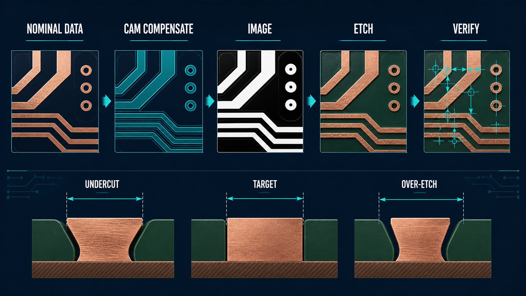
PCB etch compensation workflow from nominal design data through CAM, imaging, etching and verification
Compensation is applied before imaging and confirmed against the finished copper—not assumed from the edited artwork.

Controlled Impedance and RF Risks

Finished trace geometry contributes to impedance, loss and phase behavior, so compensation must support the released electrical target rather than a cosmetic width. Copper thickness, sidewall shape, dielectric height and material properties interact.

When tolerances are tight, provide the stackup, target impedance, relevant net classes and coupon requirements. The fabricator can model the manufacturable geometry and return a stackup/width proposal for approval. See the impedance-control PCB guide for the complete handoff.

Do not silently change controlled traces to meet a generic minimum. A proposed width change can affect routing clearance, coupling and delay and therefore needs design review.

Need a CAM and impedance DFM review?

Send ODB++ or Gerber, stackup, copper by layer, finished trace/space requirements, impedance table and critical footprint constraints. EBest Circuit can identify where production compensation may require your approval.

How CAM Engineers Build a Compensation Plan

  1. Import and verify the released revision, units and layer mapping.
  2. Confirm stackup, copper thickness and outer-layer plating route.
  3. Classify critical traces, spaces, pads, planes and impedance features.
  4. Run DFM checks for minimum finished geometry and clearance.
  5. Apply controlled layer/feature compensation based on qualified process data.
  6. Check the modified image for new shorts, clearance loss or footprint distortion.
  7. Return design-impacting exceptions for customer approval.
  8. Image, etch and measure representative production coupons/features.
  9. Feed verified results into controlled process maintenance.

The customer should be able to distinguish routine manufacturing optimization from an engineering change. Revision and approval records prevent future lots from using an obsolete interpretation.

What to Review in DFM and First-Article Evidence

  • released file checksum/revision and layer map;
  • nominal versus proposed critical feature dimensions;
  • minimum finished trace and spacing;
  • copper thickness and process route by layer;
  • impedance line widths and approved stackup;
  • fine-pitch pad and solder-mask clearances;
  • measurement method and sampling locations;
  • coupon correlation to product features;
  • exceptions requiring customer approval;
  • first-article and ongoing process-control evidence.

A report that shows only the production artwork does not prove finished geometry. Ask for measurements after the relevant plating and etching sequence.

Common Etch-Compensation Mistakes

Mistake Risk Prevention
Using one universal offset Layer and feature classes finish differently Use qualified layer/feature rules
Designer and CAM both compensate Double enlargement Declare ownership and any pre-adjustment
Ignoring finished copper route Wrong outer-layer assumption Confirm plating and copper table
Expanding pads without clearance check Mask/copper spacing or shorts Rerun full DFM after modification
Approving only a nominal coupon Product features remain unrepresented Correlate coupon, layer and density

Data to Include in an RFQ

  • ODB++ or Gerber and controlled fabrication drawing;
  • complete stackup and copper requirements by layer;
  • minimum finished trace/space and critical neck-downs;
  • controlled-impedance table and tolerance;
  • fine-pitch footprint and clearance constraints;
  • surface finish, quantity and panel requirements;
  • coupon, cross-section and measurement requirements;
  • first-article approval and report expectations;
  • delivery target and revision-control contact.

Quote finished geometry, not a guessed CAM offset

Provide nominal design data and finished requirements. We will review the manufacturing route and flag any compensation-related change that affects impedance, spacing or footprints.

FAQ About PCB Etch Compensation

What is PCB etch compensation?

It is a controlled production-artwork adjustment used to offset expected copper loss during etching so finished features meet the released target.

Should designers enlarge every trace?

Usually no. Release nominal functional geometry and let the fabricator apply its qualified process rules unless a specific exception is agreed.

Is compensation the same on every layer?

No. Copper thickness, inner/outer route, plating and feature density can change the required treatment.

What is etch undercut?

It is lateral copper removal beneath the resist edge, which contributes to tapered sidewalls and reduced width.

Does thicker copper need more compensation?

It often changes the etch challenge, but the actual rule is process- and feature-specific rather than a universal value.

Can compensation change impedance?

Yes. Finished width and sidewall geometry contribute to impedance, so critical changes should be coordinated with the approved stackup model.

Can pads be compensated like traces?

Pad changes must also preserve pitch, adjacent-copper, solder-mask and assembly clearances; a trace rule cannot be applied blindly.

How is compensation verified?

Measure finished production coupons or representative features using the agreed method after the applicable process sequence.

Should compensated CAM data be returned?

Agree the data/approval policy in advance. At minimum, design-impacting exceptions and the controlled revision should be documented.

What causes compensation to change between builds?

Material, copper, stackup, equipment, chemistry, artwork density or process-route changes can trigger review or requalification.

Final Release Checklist

  • Release nominal design intent and finished requirements.
  • Confirm copper and process route by layer.
  • Identify impedance and fine-feature constraints.
  • Assign compensation ownership and prevent double adjustment.
  • Rerun DFM on modified production artwork.
  • Approve any change affecting electrical or assembly intent.
  • Measure representative finished features.
  • Preserve revision, approval and process-control records.

Request a PCB CAM, stackup and quotation review.

Send ODB++ or Gerber, stackup, copper table, impedance requirements, critical geometry, quantity and delivery target to sales@bestpcbs.com, or use the PCB quote form. EBest Circuit will review manufacturability and identify any design-impacting CAM exception before production.

You may also like

PCB Controlled Depth Drilling for Via-Stub Control and Reliable Fabrication
Saturday, September 5th, 2026
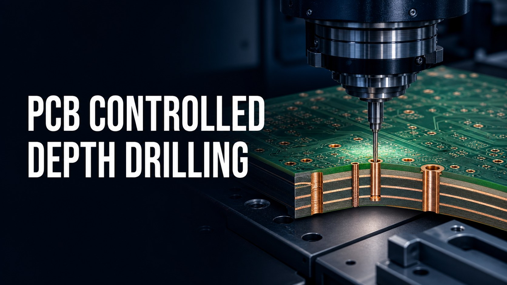
CNC spindle performing controlled depth drilling on a multilayer PCB cross-section
Controlled-depth drilling removes an unused plated via barrel only when the stackup, drill side and target layer are clearly defined.

PCB controlled depth drilling, commonly called backdrilling, removes the unused section of a plated through-hole barrel after the electrical connection layer. The remaining copper cylinder is a via stub. At high edge rates, that stub can behave as a resonant branch, increasing reflection, insertion loss or jitter.

Backdrilling is not a default requirement for every multilayer PCB. Use signal-integrity analysis to identify the vias that need it, then release exact drill side, target layer, hole group and inspection criteria to the fabricator. A note that only says “backdrill high-speed vias” is not manufacturable enough.

What Is PCB Controlled Depth Drilling?

Controlled-depth drilling is a secondary mechanical drilling operation that enters a plated hole from one board face and stops at a defined Z-depth. For via-stub removal, the secondary drill is larger than the finished plated hole so it removes unwanted copper barrel without creating a new electrical connection.

The active via section remains between the signal transition and the opposite required connection. The removed section becomes a non-plated cavity. Because the drill approaches a real copper layer, depth accuracy, registration and stackup thickness variation all matter.

“Controlled-depth drilling” can also describe other depth-limited machining. On a fabrication drawing, state that the feature is backdrilling for via-stub removal and define the layer pair. That prevents confusion with controlled-depth blind holes or mechanical recesses.

When Does a Via Stub Justify Backdrilling?

Backdrilling is justified when the predicted or measured channel penalty from the unused barrel exceeds the design budget and a simpler architecture cannot remove it. Data rate alone is an unreliable trigger because transition rise time, stub length, dielectric properties and channel topology interact.

  • Model the connector, package, trace, via transition and unused barrel together.
  • Check return loss, insertion loss and resonance over the required frequency range.
  • Identify only the nets whose stubs materially affect the channel.
  • Consider whether changing the signal layer, using a blind via or shortening the through connection solves the problem.
  • Confirm the improved design still meets power, mechanical, test and cost constraints.

Typical candidates include high-speed serial links, fast memory channels and dense connector fields. Low-speed controls and power vias usually do not need the same treatment unless analysis finds a specific issue.

Backdrilling vs Blind Vias, Microvias and Sequential Lamination

Choose the interconnect structure during stackup planning, not after routing is complete. Backdrilling preserves a through-hole manufacturing route while removing selected unused barrels. Blind or microvia structures avoid the long barrel by connecting fewer layers, but add their own build-up and reliability constraints.

Option Best fit Main tradeoff
Backdrilled through via High-layer board needing through-via routing with selected stub removal Secondary drilling, larger clearance and depth verification
Blind mechanical via Connection from a face to a defined internal layer Depth/aspect-ratio and lamination constraints
Laser microvia Short adjacent-layer HDI connections and fine-pitch escape Sequential build-up, stacking rules and qualification
Through via without backdrill Channels that tolerate the remaining stub Lowest process complexity but potential SI penalty

For structure selection, compare this guide with blind vias in HDI design, the broader PCB via types guide, and the HDI PCB fabrication guide when sequential structures are under review.

Which Vias Should Be Backdrilled?

Create an explicit backdrill set from the routed nets and stackup; do not select holes by diameter alone. Two identical through holes can require different treatment because their signal transitions end on different layers.

  • Identify the net and via designator or tool group.
  • Confirm the first and last electrically connected layers.
  • Determine whether the unused barrel is above, below or on both sides of the active connection.
  • Exclude component pins or vias whose barrel is still electrically required.
  • Check nearby copper, planes, anti-pads and adjacent holes against the larger backdrill.
  • Group only holes that share the same drill side, target layer and permitted depth window.

A separate table for each group is easier to inspect than one global note. If both sides are drilled, use distinct tool names and views.

How to Define Drill Side and Target Layer

Every controlled-depth drill group needs a physical entry side and an unambiguous stopping relationship to the last active layer. Layer names such as L10 are meaningful only when the controlled stackup revision is attached.

  1. Freeze the numbered stackup and identify top and bottom orientation.
  2. For each via, mark the signal transition and the unused barrel direction.
  3. Specify backdrill from top or bottom.
  4. State the last active layer and the layer the drill must not damage.
  5. Define the acceptable residual stub or depth window from SI and fabrication agreement.
  6. Assign a unique drill tool/group and include it in the drill legend.
  7. Cross-check the NC data, fabrication detail and net list before release.

Do not define only an absolute machine depth if the board thickness or stackup can change. Tie the requirement to the functional layer and let the approved manufacturing data translate it into the controlled drill depth.

How Much Residual Stub Is Acceptable?

Acceptable residual stub is a channel-design decision constrained by manufacturing depth tolerance. There is no universal value that fits every material, layer count, edge rate and loss budget.

A shorter stub generally moves its resonance higher and reduces its effect in the operating band, but demanding an unnecessarily small remainder can increase the risk of drilling into the capture layer or active connection. The specification needs margin for dielectric-thickness variation, copper thickness, lamination movement, drill setup and measurement uncertainty.

Use the SI model to set the maximum electrical remainder, then ask the fabricator for a safe production window. Record both the target and acceptance method. EBest-specific values are to be confirmed from the original factory capability data for the selected stackup.

How Backdrill Diameter Affects Pads and Clearances

The secondary drill is larger than the plated hole, so it consumes more radial space than the original via. Copper that was safe around a normal through hole may be cut or exposed by the backdrill.

  • Define the backdrill tool independently from the finished hole.
  • Check anti-pad clearance on every traversed layer.
  • Remove nonfunctional pads only through an approved stackup and fabricator rule.
  • Protect the required capture pad at the last active layer.
  • Review adjacent traces, plane islands, via pairs and connector pin fields.
  • Include drill wander and layer registration in the clearance analysis.

Do not copy a universal oversize. Drill diameter, plating, registration and breakout rules vary by build. Use a board-specific DFM check.

Why the Released Stackup Must Control the Backdrill

Backdrill depth is inseparable from the physical stackup. A change to prepreg thickness, core construction, copper weight or layer numbering can move the active layer relative to the board surface.

Use one revision-controlled stackup across CAD, SI analysis, fabrication drawing and NC drill output. If the fabricator proposes a material or thickness substitution, repeat the depth and residual-stub review before approval. A substitution acceptable for impedance may still change backdrill margin.

For broader release discipline, use the PCB DFM checklist. Backdrill should be part of the same controlled stackup review, not a note added after CAM preparation.

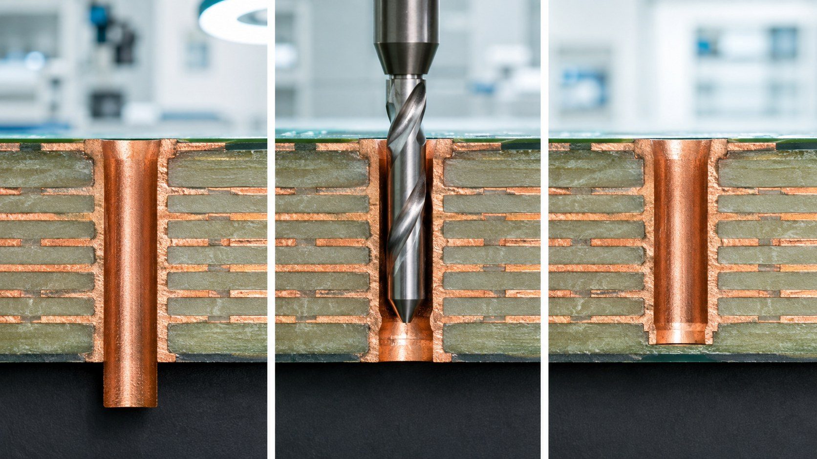
Before, drilling and after cross-sections of a plated PCB via stub removed by backdrilling
The secondary drill removes the unused barrel while leaving controlled separation from the last active connection.

What Gerber, Drill and Fabrication Notes Must Show

The released package should allow CAM to identify every backdrilled hole, its direction and its layer relationship without inference. Provide:

  1. A numbered, dimensioned stackup with material and finished thickness.
  2. Normal NC drill data and separate controlled-depth drill files or clearly identified tool groups.
  3. A backdrill table listing group, entry side, source hole/tool and last active layer.
  4. The agreed residual-stub or depth requirement and tolerance source.
  5. Backdrill diameter or a requirement for supplier calculation/approval.
  6. Cross-section details for top, bottom and double-sided cases.
  7. Inspection, coupon, microsection or depth-report requirements.
  8. A note that any stackup revision requires backdrill revalidation.

ODB++ or IPC-2581 may carry richer relationships, but a human-readable table remains valuable for quotation and independent review.

How Controlled Depth Drilling Is Manufactured

A typical backdrill route forms and plates the through hole first, then uses controlled registration and Z-depth to remove the unwanted barrel. Exact process order depends on the board construction and factory.

The manufacturer converts the layer-based requirement into a machine depth using the actual stackup. Optical or mechanical registration aligns the larger tool with the existing plated hole. The operation may be completed from one or both sides. Panels then proceed through the remaining route, finishing and inspection steps defined for the product.

Tool wear, panel flatness, entry material, spindle control and stackup variation influence the result. Capability should therefore be confirmed for the actual material, thickness and hole field rather than inferred from a generic equipment list.

How Backdrilled Vias Should Be Inspected

Inspection must prove both that enough stub was removed and that the active connection was not damaged. Select evidence according to product risk and volume.

  • CAM/drill-file reconciliation for every controlled-depth group.
  • First-article depth verification using a qualified measurement method.
  • Microsection or representative coupon showing residual stub and layer separation.
  • Visual checks for offset, breakout, debris or damaged surface pads.
  • Electrical test for opens and shorts after drilling.
  • TDR or channel testing when performance evidence is contractually required.
  • Lot, panel and tool traceability in the inspection report.

Agree on sample quantity and location before production. One convenient coupon may not represent the deepest group or densest connector field.

What Causes Overdrill, Long Stubs and Wrong-Layer Damage?

Failure Likely cause Prevention
Residual stub too long Shallow depth, stackup mismatch or conservative machine target Approved depth window and representative verification
Active pad/barrel damaged Excessive depth or wrong target layer Layer-based definition, stackup control and margin
Backdrill offset Registration error or incorrect tool alignment Fabricator clearance rule and positional inspection
Adjacent copper cut Oversize drill not included in all-layer DFM Use the real backdrill diameter in clearance checks
Wrong holes drilled Ambiguous grouping or revision mismatch Unique tool files, table and independent CAM review

How to Validate Signal-Integrity Improvement

Prove the improvement against the same channel budget that justified backdrilling. Compare modeled designs with and without the residual stub, including realistic via geometry, material properties and connector/package models.

For prototypes, correlate TDR, insertion/return loss or system eye/bathtub measurements with the fabricated stackup and inspection evidence. If measured behavior differs from simulation, check the actual residual stub, dielectric construction, via field and launch before assuming the concept failed.

Backdrill is one channel element. Trace loss, reference discontinuities, connector launches, crosstalk and equalization may still dominate.

What Changes Backdrilling Cost and Lead Time?

Cost depends on the number of drill groups, sides, depths, holes, panel setup and verification requirements. Many holes at one controlled depth can be simpler than a smaller quantity split across several target layers and both board faces.

Lead time can increase for stackup engineering, dedicated programs, first-article setup, microsections or external SI testing. Tight, unsupported tolerances can add risk without improving the channel. Ask suppliers to separate normal fabrication, controlled-depth setup and special inspection so competing quotes use the same scope.

What to Send in a Controlled-Depth Drilling RFQ

  • Gerber, ODB++ or IPC-2581 data and complete NC drill files.
  • Released numbered stackup, material, finished thickness and copper weights.
  • Backdrill table with via group, net, entry side and last active layer.
  • Target/maximum residual stub and the SI basis for it.
  • Proposed drill diameter or request for fabricator recommendation.
  • All-layer pad, anti-pad and copper-clearance data.
  • Quantity, panel constraints and prototype/production stage.
  • Electrical test, microsection, coupon, depth report and TDR requirements.
  • Change-control requirement for stackup or drill-program revisions.
  • Target delivery date and acceptance source.

Do not assume a supplier supports the same residual stub or depth tolerance across all constructions. Request written confirmation for the proposed build.

FAQ About PCB Controlled Depth Drilling

Is controlled depth drilling the same as PCB backdrilling?

For high-speed via-stub removal, the terms are commonly used together. Controlled-depth drilling can also describe other depth-limited holes, so specify the backdrill purpose and layer relationship.

Why are via stubs a signal-integrity problem?

An unused plated barrel is a branch off the signal path. At sufficiently fast transitions it can resonate and increase reflection and loss.

Does every high-speed via need backdrilling?

No. Use channel analysis to identify material stubs. Some vias are short enough, connect near the far face or can use another structure.

Can backdrilling be done from both PCB sides?

Yes when the active connection lies between unused barrel sections, but each side needs its own group, depth and clearance review.

How is backdrill depth specified?

Prefer a layer-based requirement tied to the released stackup, plus an agreed residual-stub or depth window and inspection method.

Why is the backdrill tool larger than the plated hole?

It must remove the copper barrel reliably despite normal registration variation. The selected oversize also drives anti-pad and adjacent-copper clearance.

Can a backdrill damage the signal layer?

Yes if depth, stackup, orientation or target layer is wrong. Manufacturing margin and verification protect the last active connection.

How do you inspect residual via stub?

Depending on the requirement, manufacturers may use depth measurement, coupons, microsections and electrical or TDR evidence.

Is backdrilling cheaper than microvias?

It depends on the layer structure, hole groups, lamination route and volume. Compare complete stackup and inspection costs, not one operation.

What causes most backdrill quotation delays?

Missing stackup revision, unclear drill side, no last active layer, mixed hole groups and an unsupported residual-stub requirement are common causes.

Need a multilayer PCB quote with controlled-depth backdrilling?

Send EBest Circuit your Gerber/ODB++ data, released stackup, backdrill table, drill sides, target layers, residual-stub requirement, inspection plan, quantity and delivery target. We will review the project and confirm the applicable factory route before quotation.

Send your backdrill RFQ package | Contact EBest Circuit

You may also like

PCB Edge Plating Design Guide for RF, EMC and Reliable Fabrication
Saturday, September 5th, 2026
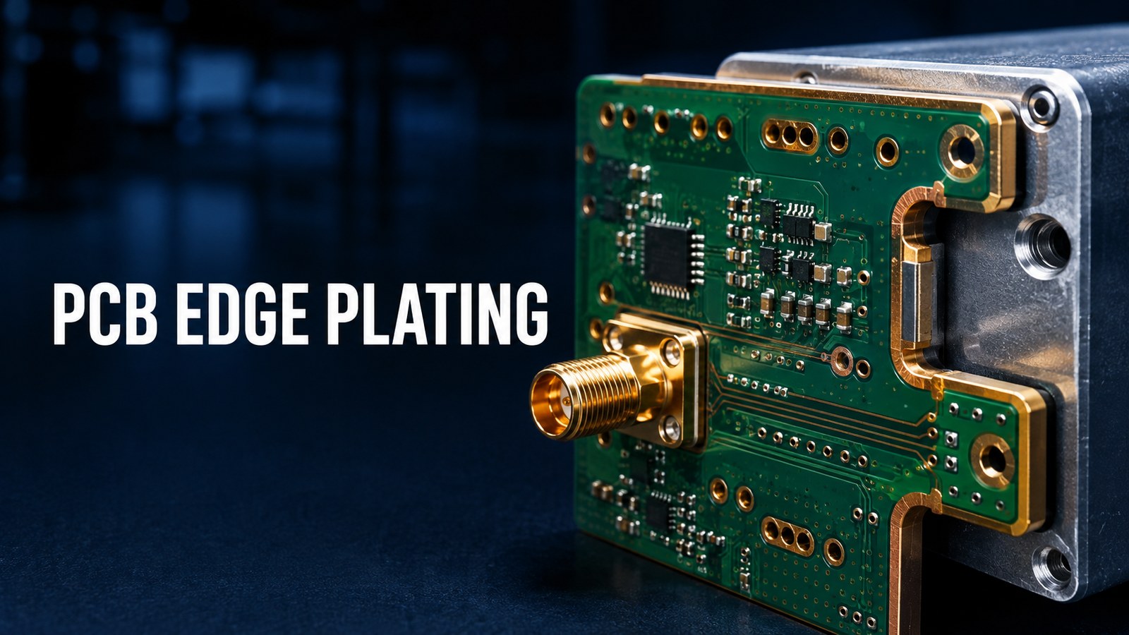
RF circuit board with conductive copper edge plating mounted in a metal enclosure
Edge plating can create a conductive connection around a routed PCB perimeter, but the layout, net assignment and panel route must agree.

PCB edge plating is copper and final finish carried from the top or bottom conductor around a routed board edge. It is used for purposes such as RF shielding continuity, chassis grounding, mechanical contact or a plated boundary. The feature succeeds only when the copper artwork, board profile, solder-mask opening, net assignment and production panel all describe the same intent.

The safest design approach is to treat the plated edge as a manufactured three-dimensional feature—not as a decorative line on one Gerber layer. Define which edges are plated, which net owns them, where plating must stop and how the fabricator may support the board during processing. This PCB edge plating design guide turns those decisions into a DFM- and RFQ-ready package.

What Is PCB Edge Plating and When Is It Worth Using?

Edge plating wraps conductive metal over a selected external board edge so it connects intended copper features on the board faces. Depending on the design, it can close part of an RF shield boundary, provide a low-inductance connection to an enclosure, create a durable contact surface or join top and bottom ground regions along the perimeter.

It is worth specifying when the electrical or mechanical function genuinely requires a plated routed edge. It is not automatically better than perimeter vias, a metal frame, a connector shell or castellated holes. Each alternative creates a different current path, assembly interface and manufacturing constraint.

  • Good candidates: RF modules fitted into conductive housings, shielding partitions, grounding rails and board edges intended to contact a conductive chassis.
  • Questionable candidates: cosmetic gold edges, edges broken by many panel tabs, mixed-net copper near the route or designs without a defined mating interface.
  • Required decision: state the electrical purpose and the mating condition before drawing the feature.

Edge Plating vs Castellated Holes and Edge Contacts

These features can all expose metal at a PCB edge, but they solve different problems. Selecting the wrong one can create unnecessary cost or an interface that cannot be assembled reliably.

Feature Main purpose Key data to define
Continuous or selective edge plating Conductive wrap, shielding boundary, chassis or mechanical contact Plated segments, net, profile, panel breaks and finish
Castellated holes Solderable half-holes for mounting one PCB onto another Hole size, pitch, pad geometry, finished profile and assembly fillet
Edge-card contacts Mating fingers for a connector Contact pattern, bevel, finish, mask opening and connector tolerance
Via fence near an edge Ground stitching and field containment without a plated route Via pitch, return-path geometry and distance to profile

A design may combine a via fence with edge plating, but their roles should remain explicit. If the real requirement is a solderable board-to-board interface, use a controlled castellated-hole design rather than asking a fabricator to infer it from a plated outline.

How Edge Plating Supports RF Grounding and EMC

A grounded plated edge can reduce discontinuity around a board perimeter and provide a short connection between face copper and a conductive enclosure. This is useful where RF currents need a controlled return path or where an enclosure seam should not become an unintended slot antenna.

Edge plating is not a universal EMI cure. Its effect depends on the full current path: reference planes, stitching vias, enclosure contact pressure, apertures, connector bonding and the location of high-frequency sources all matter. A continuous-looking copper edge that is poorly connected to the intended reference can add metal without fixing the actual return-path problem.

Start with the electromagnetic function, then model or review the transition. The site’s RF PCB capability overview provides context for high-frequency board construction, while this guide focuses on the plated boundary itself.

Should the Plated Edge Connect to System Ground or Chassis Ground?

Assign the plated edge to the net required by the product grounding architecture; do not default to a generic ground symbol. Signal ground, protective earth and chassis can be joined directly, joined through a defined network or kept separate depending on safety, EMC and system requirements.

  • Show the plated edge on the schematic or controlled mechanical/electrical drawing with a named net.
  • Identify where the edge contacts the housing and whether contact is continuous or limited to selected zones.
  • Keep unrelated power or signal copper away from the plated route according to the approved DFM clearance.
  • Review connector shields and mounting hardware as parts of the same grounding path.
  • If chassis and circuit ground are intentionally separated, mark the isolation boundary clearly.

For high-frequency designs, the via pattern that connects surface copper to internal reference planes may be as important as the plated edge. Ask for a stackup-aware review instead of applying a copied spacing rule from another board.

How to Draw Edge Copper in the PCB Layout

Draw copper to the intended finished outline on the participating outer layers and identify every plated segment unambiguously. Exact artwork conventions vary by fabricator and CAD export, so the released drawing must explain how the data should be interpreted.

  1. Create the final board profile on a single authoritative mechanical layer.
  2. Extend the intended top and/or bottom copper to the selected profile segment.
  3. Assign the copper to the correct ground, chassis or functional net.
  4. Add the required stitching connection to internal planes where the electrical design calls for it.
  5. Stop all different-net copper before the route using the fabricator-approved clearance.
  6. Mark start and stop points for selective plating, especially near cutouts and connectors.
  7. Add a detail view showing the wrap direction and finished condition.

Do not place an oversized copper flood around the entire outline if only two short edges need plating. Selective geometry makes electrical review, panel planning and inspection clearer.

Where Solder Mask Must Open Along the Plated Edge

Solder-mask data must expose the metal that is intended to wrap or make contact, while protecting adjacent copper that should remain insulated. The opening should be coordinated on both board faces and around corners or cutouts included in the feature.

Define whether the exposed band is a functional contact surface or simply part of the manufacturing wrap. If a metal enclosure, spring finger, gasket or conductive adhesive will touch it, show the actual contact footprint and tolerance zone. Keep silkscreen legends and reference text out of that interface.

Do not publish a universal mask expansion value. Registration capability, profile tolerance, finish and board construction differ. Request the approved relationship among finished edge, outer-layer copper and mask opening during DFM.

How to Keep Edge Connectors and Different-Net Copper Safe

The plated route must not unintentionally bridge a connector contact, mounting feature or nearby conductor. Edge-card fingers, coaxial launches, antenna structures and chassis contacts deserve an explicit keep-out review.

  • Separate plated segments from edge-card fingers and their bevel region.
  • Mark every intentional electrical break in the edge plating.
  • Review plated slots or cutouts independently from the external perimeter.
  • Check copper on all layers, not only the visible outer faces.
  • Confirm that a router transition or corner radius will not leave a copper bridge.
  • Include mounting holes, metal hardware and conductive gaskets in the clearance analysis.

Why Panel Tabs and Routed Breaks Must Be Planned

Edge plating requires access to the board edge, while production panels require material that holds the board during fabrication and assembly. A support tab placed through a functional plated segment interrupts the finished metal and can leave a rough breakout. A fully plated perimeter may therefore conflict with the proposed panel route.

The designer does not need to invent the factory panel, but should identify critical no-tab zones and acceptable break locations. The fabricator can then choose a routed panel, temporary support strategy or agreed interruptions compatible with its process.

Panel concern Possible result Data needed
Tab crosses plated segment Missing metal or rough witness after depanelization Critical continuous zones and permitted breaks
Insufficient handling support Board movement or process instability Array drawing and assembly handling needs
Late profile revision Copper and route no longer align One released outline revision
Corner or cutout ambiguity Unplated gap or unintended bridge Enlarged edge detail and finish callout
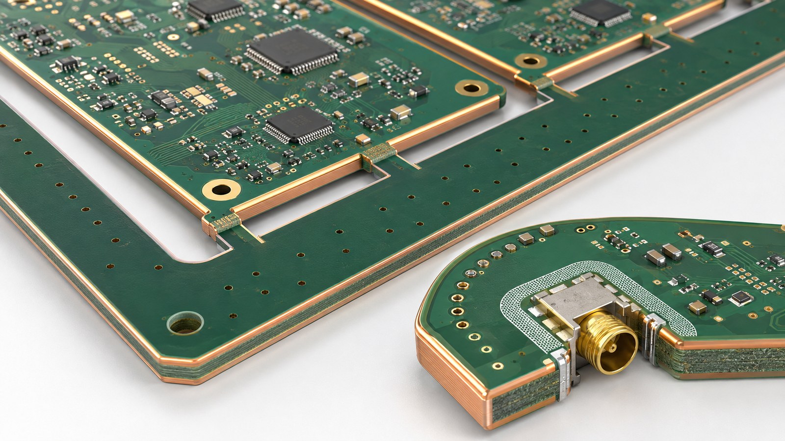
Panelized circuit boards showing plated routed edges, support tabs and connector keep-outs
Panel support, routed openings and connector keep-outs must be reviewed together with the plated segments.

How Material, Thickness and Edge Geometry Affect Feasibility

Feasibility depends on the specific stackup, board thickness, copper construction, profile geometry and factory route. Straight external edges are generally easier to define and inspect than narrow internal cutouts, acute corners or small isolated plated segments.

Before quotation, ask the supplier to confirm the proposed edge feature against the released stackup. Items that may change the route include hybrid RF materials, very thin or thick boards, heavy outer copper, sequential structures, controlled-depth features and tight mechanical interfaces.

EBest Circuit’s exact limits for a particular edge-plated build should be treated as to be confirmed through the original capability data and project DFM review. Do not assume that a value used on one material, plant or special process applies to every order. The broader PCB design for manufacturability guide explains why stackup and profile constraints should be reviewed together.

Which Surface Finish Should Be Specified?

Select the finish from the electrical contact, solderability, durability, storage and system requirements—not from edge plating alone. A plated edge that only completes a shield boundary may have different wear requirements from a repeated mechanical contact.

  • State whether the edge is a mating contact, solderable feature, enclosure interface or non-contact shield boundary.
  • Identify any wear, corrosion, bonding or conductivity requirement.
  • Confirm that the chosen finish can be applied consistently to the intended edge geometry.
  • Keep connector fingers and their finish specification separate when they use a different construction.
  • Define inspection expectations for coverage and exposed base copper.

For a general comparison of finish choices, use the PCB surface-finish selection guide. The final selection still requires project-specific confirmation.

What Gerber Layers and Fabrication Notes Should Show

A quote-ready package identifies the plated segments in both machine-readable artwork and a human-readable drawing. Do not rely on an email sentence after the data has been released.

  1. Provide Gerber, ODB++ or another agreed manufacturing dataset.
  2. Include one controlled board-profile layer with slots and cutouts.
  3. Show outer-layer copper reaching each intended plated edge.
  4. Show solder-mask openings associated with the feature.
  5. Label the electrical net and any deliberate breaks.
  6. Dimension critical contact zones, no-tab zones and mating locations.
  7. Specify surface finish and the expected finished appearance.
  8. Add a fabrication note such as “plate only the highlighted routed edges; all other edges remain unplated,” then reference the correct detail.

Include a neutral 3D image or PDF detail for communication if useful, but make the controlled fabrication data authoritative. The PCB fabrication specifications checklist can help organize the rest of the build package.

Which DFM Failures Cause Gaps, Peeling, Shorts or Rough Edges?

Most edge-plating failures begin as a disagreement among the electrical design, mechanical profile and panel route. Review the failure mechanism before changing only the visible copper artwork.

Symptom Likely question Prevention
Gap in a critical segment Did a tab, route transition or artwork break cross the edge? Define continuous zones and review panel support
Unintended short Was another net or connector feature too close to the plated route? Run all-layer clearance and net checks
Peeling or weak adhesion Does the copper construction and process support the geometry? Confirm stackup and edge preparation with the fabricator
Rough breakout Was a functional surface used as a depanelization point? Move tabs or define an acceptable non-contact break
Finish does not cover as expected Was the edge included in the finish and inspection callout? State the finished condition and acceptance criteria

How Should Edge Plating Be Inspected and Accepted?

Acceptance should address coverage, continuity, isolation, finish and mechanical interface. Visual appearance alone cannot prove the intended electrical function.

  • Verify the correct edges and only those edges are plated.
  • Inspect critical segments for gaps, exposed base material, blisters, peeling and rough damage.
  • Check isolation from different-net copper and adjacent connector contacts.
  • Measure continuity or resistance where the drawing defines an electrical requirement.
  • Fit-check the enclosure, spring contact or gasket when the edge is a mechanical interface.
  • Record first-article photographs of critical corners, breaks and contact zones.
  • Agree in advance how permitted panel-break witness marks will be judged.

For RF hardware, functional verification may also include enclosure-level EMC or RF testing because a good-looking edge cannot compensate for gaps elsewhere in the shield or return path.

What Changes Edge-Plating Cost and Lead Time?

Cost and lead time depend on plated length and complexity, stackup, routing, panel support, finish, inspection and first-article requirements. Selective straight segments with clear data are easier to assess than a nearly continuous perimeter broken by connectors, tabs and internal cutouts.

Ambiguous data adds engineering exchanges and can delay quotation. A special panel strategy, unusual finish, tight contact tolerance or additional electrical/mechanical inspection can add setup and processing time. Ask suppliers to separate non-recurring engineering or tooling from recurring unit cost so quotes can be compared on the same assumptions.

What to Send for an Edge-Plating RFQ

The RFQ must let the supplier reconstruct the electrical, mechanical and manufacturing intent without guessing. Send:

  • Gerber or ODB++ data, drill files and one authoritative board profile.
  • Stackup, material selection, finished thickness and copper requirements.
  • A drawing that highlights every plated segment and intentional break.
  • The plated-edge net and its connection to planes or stitching vias.
  • Solder-mask openings, connector keep-outs and enclosure contact zones.
  • Permitted and prohibited panel-tab locations.
  • Surface finish and any wear, bonding or corrosion requirement.
  • Quantity, prototype or production stage and target delivery date.
  • First-article, continuity, dimensional and visual acceptance requirements.
  • BOM, CPL and assembly drawings when fabrication and assembly will be quoted together.

Label unresolved items as “supplier to confirm” rather than silently assuming a factory limit. That makes the DFM response part of the controlled engineering record.

FAQ About PCB Edge Plating

Is PCB edge plating the same as castellated holes?

No. Edge plating creates a conductive wrap along a routed edge, while castellated holes form solderable half-holes for board-to-board assembly. Their artwork and acceptance criteria differ.

Does edge plating always need to connect to ground?

No. Grounding is common for shielding and chassis interfaces, but the correct net follows the product architecture. State the intended net explicitly.

Can an entire PCB perimeter be edge plated?

Potentially, but production panel support and depanelization must still be solved. A nominally continuous perimeter may require agreed breaks or a special handling route.

Can edge plating improve EMC?

It can support a shorter, more continuous shielding or return path, but EMC performance depends on the entire enclosure, planes, via stitching, connectors and apertures.

Should copper extend to the board outline?

For intended edge-plated segments, outer-layer copper is typically designed to meet the finished route according to the fabricator’s data convention. Confirm the exact artwork rule during DFM.

Should solder mask cover a plated PCB edge?

A functional plated contact normally requires a coordinated mask opening. The correct opening depends on the intended contact and the supplier’s registration and process rules.

Why do panel tabs matter?

A tab can interrupt a plated segment and leave a rough witness after breakout. Mark critical no-tab zones and permitted breaks before the array is finalized.

Which surface finish is best for edge plating?

There is no universal choice. Select the finish from conductivity, wear, solderability, corrosion and mating requirements, then confirm it for the edge geometry.

How is edge plating inspected?

Inspection can include visual coverage, continuity, isolation, dimension and fit with the mating enclosure or contact. Define the required evidence in the drawing or quality plan.

What is the most important RFQ detail?

A marked fabrication detail showing exactly which edges are plated, their net, the finish and acceptable panel breaks. Without it, the supplier must guess at the core requirement.

Need a PCB quote with edge plating?

Send EBest Circuit your Gerber/ODB++ files, stackup, plated-edge drawing, net assignment, surface finish, panel constraints, quantity and acceptance requirements. We will review the project data and confirm the applicable manufacturing route before quotation.

Send your edge-plating RFQ package | Contact EBest Circuit

You may also like

PCB Peelable Solder Mask: When to Use It and How to Specify It
Saturday, September 5th, 2026
PCB peelable solder mask protecting selected through-holes and contacts before removal
Peelable solder mask temporarily protects selected PCB features during assembly or coating, then is removed.

PCB peelable solder mask is a temporary masking material used to keep solder, flux, cleaning fluid or conformal coating away from selected holes, contacts and component areas. Unlike the permanent solder mask that remains on a finished PCB, the temporary film is applied for a defined process step and peeled away afterward.

It is useful only when the material, coverage, cure condition and removal plan match the assembly process. A vague fabrication note such as “add blue mask” is not enough: the supplier needs a marked layer, the protected features, the process exposure and the acceptance condition. This guide explains how to make that decision and prepare a quote-ready package.

What Is PCB Peelable Solder Mask?

Peelable mask is a removable process aid, not the PCB’s permanent dielectric coating. It is commonly supplied as a viscous liquid that is placed over selected areas, cured into a flexible film, exposed to the intended process and removed manually. Product chemistry and processing windows differ, so the selected material’s current technical data sheet controls.

The distinction matters at purchase order review. IPC-SM-840 addresses permanent solder mask and flexible cover materials; it should not be used as a blanket qualification statement for every temporary peelable compound. Define temporary masking as its own fabrication or assembly requirement, with a named purpose and an agreed acceptance check.

Layer or material Purpose End condition
Permanent solder mask Insulates and protects the finished PCB surface while exposing intended pads Remains on the board
Peelable temporary mask Blocks solder, flux or coating from selected zones during a process step Removed after the defined operation
Coverlay Protects flexible-circuit conductors and defines openings Remains as part of the FPC
Assembly tape or fixture Provides temporary mechanical masking or support Removed or reused according to the process

When Should You Use Peelable Mask on a PCB?

Use it when selected features must stay free of solder or coating while nearby areas go through the same operation. The strongest use cases have a clear protected zone, a compatible material and an accessible peel path.

  • Keep selected plated through-holes open during wave soldering for a later connector or mechanical assembly.
  • Protect edge contacts, test points, pins or terminals from solder contact.
  • Mask connectors and keep-out areas during spray, brush or dip conformal coating when the chosen product supports that exposure.
  • Temporarily cover a local area during cleaning or another documented assembly operation.
  • Reduce manual taping where repeatable dispensed or screened coverage is practical.

Do not choose it merely because it is removable. Very small, tightly packed or inaccessible zones may be difficult to coat consistently and harder to peel without fragments. High-temperature dwell, aggressive chemicals, bare-metal compatibility and cleanliness requirements must be checked against the exact product and process.

Peelable Mask vs Tape, Washable Mask and Permanent Solder Mask

The best option is the one that protects the feature through the process and can be removed without creating a new defect. Geometry, volume, temperature, chemistry and cleanliness usually decide the choice.

Option Good fit Risk to check
Peelable mask Irregular groups of holes or contacts; repeatable local coverage Minimum film body, complete cure, peel access and fragment control
High-temperature tape Simple edges or flat shapes; low-volume manual work Labor, edge leakage, adhesive residue and placement variation
Washable mask Processes with a validated compatible wash step Complete dissolution, wash chemistry and trapped residue
Reusable fixture or pallet Stable, repeated production with suitable board geometry Tooling cost, board support, clearances and revision control
Permanent solder mask Normal long-term surface protection and pad definition It cannot serve as a removable post-process mask

For a related overview of surface-protection choices, see the guide to solder mask on a PCB. For board purchasing, the broader PCB fabrication specifications checklist helps connect the mask note to the full build package.

Which PCB Areas Should Be Protected?

Mark only the features that must remain untouched by the next operation, then include enough surrounding area to form a continuous removable film. Protection zones often include through-holes reserved for a later insertion step, gold fingers, connectors, test points, terminals or coating keep-outs.

Review the zone against both sides of the board. A mask covering a hole on one side may not prevent ingress from the opposite side unless the application method and coverage are designed for it. Also check nearby solder joints, small components and board edges so the cured film can be gripped and peeled without stressing hardware.

  1. Identify the exact process the area must survive.
  2. Mark every protected feature on a dedicated drawing or unambiguous data layer.
  3. Define which board side receives the mask.
  4. Provide a clear boundary and any critical keep-out around adjacent pads or components.
  5. Confirm that the cured film has an accessible removal edge.

How Do Wave Soldering, Cleaning and Conformal Coating Affect the Choice?

A peelable mask must be selected for the complete exposure sequence, not for temperature alone. During wave soldering it may encounter preheat, flux, molten solder and cleaning. During conformal coating it may contact solvent or water-based chemistry and must resist coating ingress around the protected feature.

Manufacturer data illustrates why a generic number is risky. Techspray’s WonderMASK P documentation gives product-specific cure, thickness and wave-solder limits, while MG Chemicals 862 lists its own application and cure parameters. Those values describe those named products; they are not universal PCB design rules. The contract manufacturer must confirm the actual material, application method and validated process window.

Surface finish also matters because the protected feature may be bare copper, plated metal, a soldered surface or a gold contact. Request compatibility confirmation for the actual finish rather than assuming all peelable masks behave alike. The selection of the exposed finish itself can be reviewed separately in the PCB surface-finish selection guide.

How Should Peelable Solder Mask Be Shown in Gerber Data and Drawings?

Create a dedicated, clearly named temporary-mask layer and repeat its purpose in the fabrication or assembly drawing. Do not rely on color alone, a screenshot or a filename such as “blue glue” without a legend. The manufacturer must know whether filled shapes indicate covered areas or openings.

  1. Name the layer, for example, TOP_PEELABLE_MASK or BOTTOM_TEMP_MASK.
  2. State the polarity: “filled geometry equals mask coverage.”
  3. Identify the operation: wave solder protection, conformal-coating keep-out or another defined step.
  4. Call out the board side, protected feature and any critical boundary tolerance.
  5. State that the mask is temporary and must be removed after the specified operation.
  6. Define the post-removal acceptance condition: no unintended solder/coating on protected features, no visible mask fragments, and no damage to pads, finish or components.

Include a reference image only as a communication aid; released manufacturing data must remain authoritative. If Gerber naming or polarity is unclear, expect a DFM question before production.

Which Material and Process Limits Must the Supplier Confirm?

Ask the supplier to identify the exact temporary mask and confirm it against the board finish and assembly route. Evidence should be marked as verified, to be confirmed or unavailable. Do not turn an open capability question into a public claim.

  • Product name, revision of technical data sheet and shelf-life control.
  • Compatibility with copper, gold, silver, solder, OSP or other exposed finish in the protected zone.
  • Application method: hand dispense, template, pneumatic or robotic placement.
  • Target film build and minimum practical geometry for a continuous peel.
  • Cure condition, maximum process temperature and exposure time.
  • Resistance to the actual flux, cleaner and conformal-coating chemistry.
  • Removal method, peel access and residue/fragment inspection.
  • First-article evidence before volume production.

For quotation, treat this as a capability-to-be-confirmed item. Board type, factory route, selected material and the original process record must all be checked before a supplier commits to a production value.

Three-stage PCB peelable solder mask process showing protection, wave soldering and clean removal
A robust plan covers application, process exposure and complete removal—not just the mask artwork.

What Causes Lifting, Leakage, Tearing or Residue?

Most failures trace to surface condition, weak geometry, incomplete or excessive cure, incompatible chemistry or an uncontrolled removal step. Diagnose the mechanism instead of simply adding more material.

Symptom Likely questions Control
Edge lifting Was the surface contaminated? Was the film fully formed at the edge? Clean surface, validate application and inspect before exposure
Solder or coating leakage Was the boundary continuous? Did the process attack the mask? Confirm coverage and chemistry with a first article
Film tears during peeling Was it too thin, over-cured or trapped around geometry? Use a validated film body and accessible peel path
Fragments remain in holes Were holes bridged or filled in a way that prevents one-piece removal? Inspect both sides and use magnification where needed
Residue or finish change Is the exact material compatible with the surface and cleaner? Approve the named material and verify after removal

A preproduction board is valuable when the geometry is new, the protected finish is sensitive or the mask will see multiple chemical steps. Record the applied condition and removal result so production is not dependent on operator memory.

How Should Peelable Mask Be Inspected and Removed?

Inspect coverage before the protected operation and inspect cleanliness and feature condition after removal. The film should be removed using the method approved for the material, typically with a controlled manual peel. Do not assume a peelable mask will dissolve in the cleaning process.

  • Before processing: verify the correct board side, all marked zones, continuous edges and no interference with intended solder joints.
  • After processing: allow the board and coating, where applicable, to reach the approved removal condition.
  • Peel without levering against small components, pads or fragile flex areas.
  • Inspect holes, corners and narrow gaps for remnants.
  • Verify protected contacts remain free of unintended solder or coating.
  • Check that the surface finish, permanent solder mask and nearby components are undamaged.
  • Record first-article photographs when the mask is a critical process characteristic.

If the user intent is specifically “how to remove solder mask from PCB,” first distinguish temporary peelable mask from permanent LPI solder mask. Permanent solder mask removal is a different rework operation and may damage copper or change the board’s insulation and reliability.

What Changes Peelable-Mask Cost and Lead Time?

Cost is driven mainly by protected-area complexity, application method, inspection effort and whether the process is already validated. A few accessible holes may be straightforward; many small islands, both-side coverage, tight component clearances or repeated coat/cure cycles add labor and risk.

Lead time can increase when the material must be sourced, the drawing is ambiguous, a first article is required, or compatibility testing is needed for a special finish, cleaner or coating. Quantity changes the economic choice: manual masking can fit prototypes, while recurring production may justify a template, controlled dispensing program or solder pallet.

Ask suppliers to separate non-recurring setup from per-board masking and inspection. That makes quote comparisons more meaningful than a single total price with different assumptions hidden inside it.

What Should You Send in a Peelable-Mask RFQ?

A quote-ready package tells the supplier what to protect, what the mask must survive and how the result will be accepted. Send:

  • Gerber or ODB++ files, drill data and fabrication drawing.
  • A dedicated top and/or bottom temporary-mask layer with stated polarity.
  • PCB stackup, material, thickness, copper and surface finish.
  • Assembly drawing, BOM and CPL when the board will also be assembled.
  • Wave-solder profile or other expected temperature exposure.
  • Flux, cleaning and conformal-coating details where relevant.
  • Quantity, prototype/production stage and target delivery date.
  • Required first-article photographs, inspection report or sample approval.
  • Post-removal acceptance criteria and any cleanliness requirement.

For a complete manufacturing handoff, pair this with the site’s PCB DFM guide. A supplier can then review mask feasibility together with the board outline, holes, finish, assembly sequence and inspection plan.

FAQ About PCB Peelable Solder Mask

Is peelable solder mask permanent?

No. It is a temporary process material intended to be removed after the specified soldering, cleaning or coating operation. Permanent PCB solder mask remains on the finished board.

Why is peelable solder mask often blue or pink?

Color helps operators see coverage and, for some products, may indicate curing progress. Color alone does not identify chemistry or performance, so use the product name and current TDS.

Can peelable mask protect plated through-holes during wave soldering?

Yes, this is a common application when the selected product and coverage are validated for the wave process. Both-side access, film continuity and post-process removal still require review.

Can it protect gold fingers and contacts?

Some named products are documented for contacts or gold fingers, but compatibility must be confirmed for the exact finish, material and exposure sequence.

Is peelable mask the same as coverlay?

No. Coverlay is a permanent protective layer used on flexible circuits. Peelable mask is temporary and is removed after its process function is complete.

Can I specify only “blue mask” on the drawing?

No. State that it is temporary peelable mask, define the covered geometry and polarity, identify the board side and operation, and specify removal and acceptance requirements.

How thick should peelable solder mask be?

There is no single universal value. Each material has a product-specific recommended film build, and the practical geometry also depends on application and removal. Use the selected product’s TDS and supplier approval.

Does peelable mask leave residue?

A suitable, correctly processed product is intended to remove cleanly, but residue or fragments can occur if chemistry, cure, surface condition or geometry is wrong. Post-removal inspection is necessary.

How is temporary peelable mask removed from a PCB?

After the approved process and cooling or coating condition, it is normally lifted and peeled manually according to the material instructions. Inspect holes and tight corners for remnants.

Should the first production build include a mask sample?

Yes when the geometry, finish, chemistry or thermal route is new or critical. A first article can confirm coverage, survival, removal and the protected-feature acceptance condition before volume production.

Need a PCB quote with temporary peelable masking?

Send EBest Circuit your Gerber/ODB++ files, peelable-mask layer, surface finish, process profile, quantity and acceptance requirements. We will review the data and confirm the applicable manufacturing route before quotation.

Send your peelable-mask RFQ package | Contact EBest Circuit

You may also like