PCB manufacturing PCB manufacturing
Home > Blog

PCB Surface Finish

PCB Surface Finish Shelf Life: Storage and Assembly Guide
Saturday, September 5th, 2026
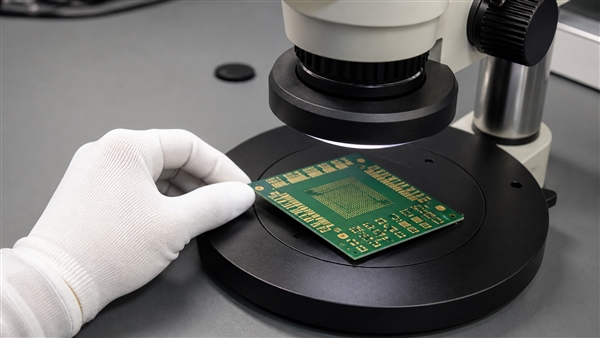
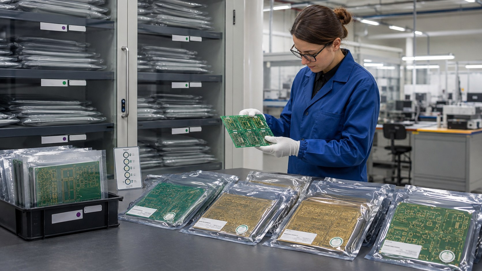
Quality engineer inspecting date-controlled bare PCBs in moisture-barrier packaging
PCB shelf-life control starts with the selected finish, packaging date, storage environment and planned assembly process.

PCB surface finish shelf life is the period during which a correctly packaged and stored bare board is expected to remain suitable for the specified assembly process without unusual restoration. It is not the same as the service life of an assembled product, and it is not a universal number printed on every board.

ENIG, HASL, OSP, immersion silver and immersion tin protect exposed copper in different ways. Their practical storage windows depend on finish quality, packaging integrity, temperature, humidity, airborne contamination, handling and the soldering process. Buyers should therefore ask for a documented shelf-life basis and an acceptance plan instead of relying on a generic online table.

What PCB Surface Finish Shelf Life Actually Means

For bare PCBs, shelf life is mainly a solderability and surface-integrity question. A date does not prove that every pad is good before it or unusable after it. It defines the manufacturer’s expected window under stated storage conditions and helps control risk.

This differs from moisture sensitivity of components, laminate moisture absorption, and the operating life of a populated assembly. Those issues can interact, but each needs its own evidence and corrective action.

Why There Is No Universal Expiration Date

The same finish name can deliver different storage performance when deposit thickness, porosity, cleanliness, packaging or handling changes. A sealed lot held in controlled storage is not equivalent to an opened bag exposed to humid or sulfur-bearing air.

  • The finish and its qualified process determine the starting protection.
  • The package barrier, desiccant and seal condition control environmental exposure.
  • Storage temperature and humidity affect oxidation and moisture uptake.
  • Fingerprints, dust and sulfur contamination can damage solderability locally.
  • Multiple openings and partial-lot use reset the practical risk assessment.

Use the supplier’s stated conditions and lot records. Treat online month ranges as planning references, not acceptance guarantees.

How Common PCB Surface Finishes Compare for Storage

Finish selection changes both the protective mechanism and the likely failure mode during storage.

Finish Storage strength Main concern before assembly
ENIG Nickel barrier with gold-protected contact surface Contamination, deposit quality and wetting verification
HASL / lead-free HASL Solder-coated surface can be robust for conventional assembly Planarity, oxidation and compatibility with fine pitch
OSP Thin organic protection with excellent flatness Handling, heat-cycle exposure and surface-film damage
Immersion silver Flat surface suitable for fine-pitch assembly Tarnish and sulfur exposure
Immersion tin Flat solderable tin surface Oxidation, intermetallic growth and handling history

For a deeper finish-selection comparison, review our PCB immersion gold guide and the OSP guidance for HDI boards.

Storage Conditions That Shorten the Usable Window

Humidity, temperature cycling, corrosive gases and careless handling can reduce usable life faster than calendar time alone. Damaged moisture-barrier bags, exhausted desiccant, unrecorded bag openings and storage near cardboard, rubber or process chemicals deserve attention.

Keep bare boards in the specified package until needed. Use clean gloves, ESD controls and a controlled staging area. Do not stack exposed boards pad-to-pad or clean them with an unapproved chemical.

Planning a build with stored or date-sensitive bare PCBs?

Send the finish, fabrication date, package condition, storage history and assembly profile. EBest Circuit can review the risk before the lot reaches the line.

Packaging and Inventory Controls That Preserve Solderability

A useful storage system is traceable, sealed and easy to audit. It should identify the lot, finish, packaging date, stated shelf life, storage condition and bag-opening history.

  1. Receive the lot and inspect the outer package, seal and labels.
  2. Record the fabrication/packaging date and supplier storage conditions.
  3. Store sealed material in the controlled location defined by the supplier.
  4. Issue inventory by lot and first-expiring-first-out logic.
  5. Record each opening, partial withdrawal and reseal action.
  6. Escalate damaged, untraceable or aged lots before assembly scheduling.
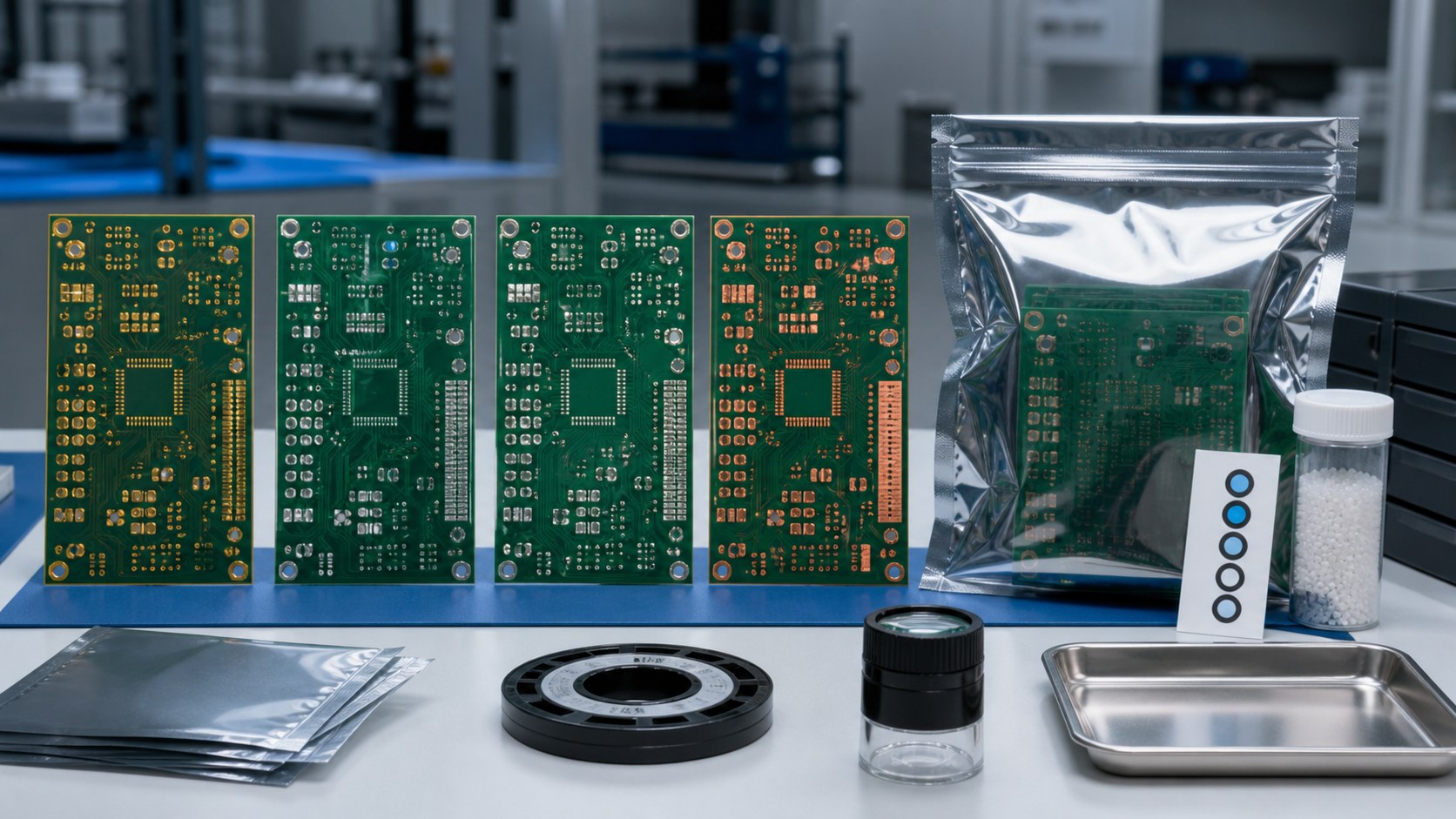
PCB finish samples beside moisture-barrier packaging and storage-control materials
Finish comparison is useful only when packaging, storage history and the planned assembly process are reviewed together.

How to Assess Boards Near or Beyond the Stated Date

Do not accept or scrap an aged lot from the date alone. Quarantine it, review traceability and packaging history, inspect representative boards and agree the required solderability evidence.

Useful checks may include visual inspection, package-condition review, surface contamination investigation and a recognized solderability test selected for the finish and assembly method. Sampling must represent the lot; one attractive board does not prove every panel is suitable.

If corrosion, discoloration, exposed copper, contamination or poor wetting appears, engineering and quality teams should decide whether controlled cleaning, rework, finish restoration or replacement is permitted. The disposition must protect pad geometry and product requirements.

When Baking Helps—and When It Does Not

Baking may reduce absorbed moisture, but it does not reverse oxidation, tarnish, contamination or a degraded surface deposit. Excess heat can also affect materials, solder mask, markings or board flatness.

Use baking only under a documented procedure compatible with the laminate, finish and board construction. Do not treat it as an automatic shelf-life reset. After any recovery action, verify the property that was actually at risk.

How Storage History Affects Assembly Yield

Surface degradation usually appears as a process problem: incomplete wetting, dewetting, nonwetting, excessive voiding, inconsistent hole fill or rework. Fine-pitch pads and demanding thermal profiles can expose marginal solderability sooner.

Before a critical build, align the board finish with solder paste, flux, stencil, component termination and reflow or wave profile. If the lot has unusual storage history, a small controlled trial can be safer than discovering the issue across a full production batch.

Need a finish that matches both storage and assembly?

Share your component pitch, soldering method, expected inventory time, compliance needs and handling environment for a finish-and-process DFM review.

How to Select a Surface Finish for Long or Uncertain Storage

Choose the finish from the whole product and supply-chain requirement, not shelf life alone. Consider pad flatness, fine-pitch assembly, wire bonding or contacts, number of thermal excursions, rework, environmental compliance, cost and expected inventory delay.

If boards may sit for months before assembly, tell the fabricator during quotation. The team can review finish suitability, package configuration, lot labeling and whether staged releases would reduce exposure. For harsh end-use environments, also review our PCB fabrication for harsh environments guide.

What to Put in the PCB RFQ and Purchase Specification

The RFQ should turn ā€œlong shelf lifeā€ into verifiable requirements. Send the Gerber or ODB++ data, fabrication drawing, stackup, board quantity, finish, compliance needs, assembly method, expected storage duration, packaging preference and acceptance standard.

  • Ask how shelf life is defined and from which date it starts.
  • State the required package, desiccant, humidity indicator and lot labels.
  • Define storage and handling conditions.
  • Agree what evidence is supplied and what triggers reinspection.
  • Identify fine-pitch, press-fit, wire-bond or contact areas with special needs.
  • Keep deviations and recovery actions subject to written approval.

How EBest Circuit Supports Finish, Packaging, and Assembly Decisions

EBest Circuit can review the finish as part of fabrication and assembly DFM rather than as an isolated coating choice. The review connects pad geometry, component technology, soldering process, expected storage, handling and inspection needs.

Send Gerber/ODB++, BOM, CPL, quantities, material and copper requirements, preferred finish, test needs and target delivery. We can flag missing requirements, discuss suitable packaging and prepare a quote based on the actual build. Specific shelf-life claims remain conditional on the approved finish specification and storage plan.

PCB Surface Finish Shelf Life FAQ

What is the typical shelf life of a bare PCB?

There is no single value for every PCB. Use the fabricator’s stated period and conditions for the specific finish, lot, packaging and storage environment.

Does an expired date mean the PCB must be scrapped?

No. Quarantine the lot and use traceability, package history, inspection and agreed solderability testing to make the disposition.

Which PCB finish has the longest shelf life?

The answer depends on qualified process quality and application constraints. ENIG and solder-coated finishes are often considered for storage robustness, but flatness, bonding, cost and assembly needs still govern selection.

Why is OSP more handling-sensitive?

OSP relies on a thin organic film over copper. Abrasion, contamination and repeated heat exposure can reduce its protection and solderability.

Can PCB baking restore an aged surface finish?

Baking addresses moisture under an approved procedure; it does not reverse oxidation, tarnish or contamination.

Should unopened bags be trusted without inspection?

Inspect package integrity, labels, seal condition and storage records. An unopened but damaged or poorly stored bag may still need escalation.

What records should follow a stored PCB lot?

Keep lot identity, finish, packaging date, stated conditions, receipt inspection, storage location, openings, reseals and disposition decisions.

Can surface finish shelf life affect reflow yield?

Yes. Marginal solderability can contribute to incomplete wetting, dewetting and inconsistent joints, especially on fine-pitch or demanding assemblies.

Is bare-board shelf life the same as component MSL?

No. Component moisture sensitivity and bare-board storage risk are separate controls, although both can affect assembly.

What should I send for a shelf-life review?

Send the board files, finish specification, lot and packaging dates, storage/opening history, photographs, planned assembly process and target schedule.

Turn shelf-life uncertainty into an assembly-ready plan.

Send your Gerber/ODB++, BOM, CPL, finish, storage history, quantity and target delivery. EBest Circuit will review finish, packaging and assembly risks before production.

You may also like

When Is PCB Immersion Gold the Right Surface Finish?
Wednesday, September 2nd, 2026

PCB immersion gold is usually an ENIG surface finish: a thin gold layer over electroless nickel on exposed copper pads. It offers a flat solderable surface and protects the nickel before assembly. It is a useful choice for many fine-pitch boards, but it is not the same as wear-resistant hard gold. The right decision depends on how the pads will be soldered, contacted, stored and inspected.

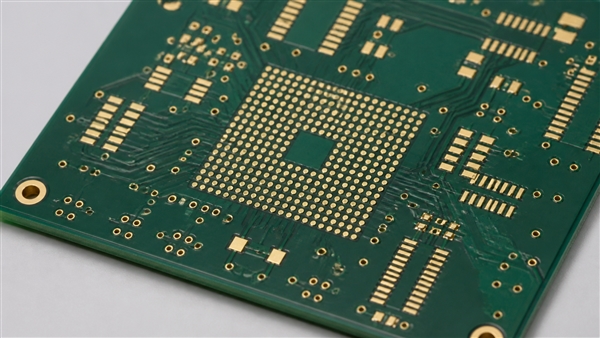
PCB immersion gold finish on flat BGA and fine-pitch solder pads

What Is Immersion Gold PCB Surface Finish?

ENIG stands for electroless nickel immersion gold. The copper carries the circuit, nickel forms the barrier beneath the finish, and gold protects that nickel from oxidation. An electroless nickel immersion gold PCB therefore has a layered coating on selected exposed conductors, not a solid-gold circuit board. An ENIG PCB retains copper as its main circuit conductor.

The terms immersion gold finish, ENIG finish and chemical nickel/gold commonly describe this construction. A gold plated circuit board is a broader description: it might use ENIG, electrolytic hard gold or another gold-containing finish. Color alone cannot identify the process, thickness or intended application. Our ENIG process overview provides further background on this finish family.

Is direct immersion gold the same as ENIG?

No. Direct immersion gold places gold directly on copper, without the electroless nickel layer that defines ENIG. It is a different finish architecture. Confirm the full coating stack whenever a drawing uses only ā€œimmersion goldā€; this article focuses on the conventional ENIG construction.

How Does the PCB Immersion Gold Process Work?

The PCB immersion gold process normally follows copper patterning and solder-mask preparation. Exposed copper is cleaned and prepared, electroless nickel is deposited, and a controlled immersion reaction deposits the gold coating. Rinsing, drying and inspection complete the finish. The exact preparation sequence depends on the qualified chemistry and board materials.

In conventional immersion gold plating, gold deposition involves a displacement reaction at the nickel surface. It does not require the external electrical connection used by electroplating. The process must balance coverage against excessive nickel attack; simply leaving a board in the bath longer is not a sound way to request better quality.

What does electroplated gold mean?

It means gold is deposited using an externally supplied electrical current. PCB gold plating can use that method to build a specified contact finish, including hard gold plating. Electroless gold plating is a broader chemistry term and should not be used to erase the difference between autocatalytic deposition and immersion displacement. Specify the actual process, not just ā€œAu plating.ā€

What Does Each ENIG Layer Do?

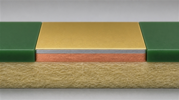
The three metals have different jobs. Copper is the underlying conductor. Nickel separates copper from the outer gold and provides the interface beneath the solderable finish. The gold cap protects the nickel during the intended pre-assembly life, but it is not an impermeable environmental seal.

Illustrative PCB immersion gold cutaway showing thin gold over nickel and copper, not to scale

During normal soldering, the thin gold coating is incorporated into the solder and the joint develops at the underlying nickel-containing interface. The finished joint should not be imagined as a solder ball resting on a permanent gold barrier. This is why nickel condition matters even when an ENIG circuit board looks uniformly gold.

How Thick Should PCB Immersion Gold Be?

Specify nickel and gold separately. Nickel thickness is on the micrometer scale, while immersion gold thickness is much smaller, typically discussed in hundredths of a micrometer. A requirement stating only ā€œgold thicknessā€ leaves the barrier layer and measurement method unresolved.

For unit checking, 1 microinch = 0.0254 micrometer; therefore, 2 microinches is 0.0508 micrometer. This is a conversion example, not a recommended acceptance limit. Never confuse micrometers with microinches or apply a connector hard-gold requirement to ENIG solder pads.

PCB immersion gold thickness requirements should identify the applicable IPC-4552 revision, agreed deposit limits, measurement locations and acceptance method. PCB ENIG specifications should also distinguish process-control targets from lot-acceptance criteria. Do not combine figures from different revisions or treat a single measurement as proof of process consistency. A brighter surface does not demonstrate a thicker or better deposit.

Does ā€œIPC 4552 Class 3ā€ define every acceptance condition?

No. The phrase identifies a standards-related requirement but is not a complete coating specification. State the revision and applicable product requirements, then confirm how deposit thickness, nickel corrosion and solderability will be assessed. Class selection does not authorize an arbitrary increase in gold thickness.

Why Choose ENIG for Fine-Pitch Assembly?

An ENIG surface finish is relatively planar, which can help solder-paste printing and component seating on closely spaced lands. This is valuable for BGA, QFN and other fine-pitch packages where an uneven finish can complicate assembly. Flatness is a useful starting condition, not a guarantee against bridging, voids or poor joints.

For HDI printed circuit boards, finish selection belongs alongside pad geometry, microvia construction and solder-mask registration. ENIG does not fill an open via-in-pad or correct a badly defined land pattern. Those features require their own manufacturing controls.

An immersion gold FR4 PCB need not be high density. On double-sided FR4 circuit boards, the same finish may be selected for flat pads and a planned assembly-storage window. Choose it because those requirements matter, not because a gold plated PCB board automatically performs better electrically.

PCB Immersion Gold vs Hard Gold Plating

ENIG is primarily selected for solderable pads and qualified low-wear interfaces. Hard gold is selected when contact wear and repeated mating drive the specification. These are different engineering jobs even if both surfaces appear gold.

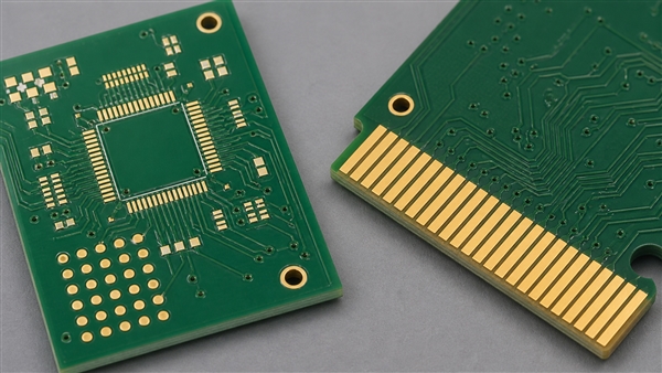
PCB immersion gold solder-pad sample beside an illustrative hard-gold edge-contact board
Requirement ENIG / immersion gold Hard gold
Primary role Flat solderable finish and qualified contacts Wear-resistant electrical contact surface
Deposition Electroless nickel with immersion gold cap Usually electrolytic gold alloy over nickel
Repeated insertion Not a default substitute for connector plating Specify thickness, hardness and mating conditions
Soldering Normal use when finish and assembly are qualified Must be assessed for the specific deposit and joint

A board may need selective hard gold on edge fingers and a different finish on solder pads. Keep these areas explicit in the fabrication definition. Do not approve a substitution using only the word ā€œgold,ā€ and do not assume a thin immersion coating will survive a connector’s full mating-cycle requirement.

ENIG vs HASL and OSP: Which Finish Fits?

Comparing PCB surface finish types starts with the assembly process. Lead-free HASL leaves a solder-alloy coating; OSP is an organic copper surface finish; ENIG adds nickel and gold. These PCB surface finishes protect exposed PCB surfaces differently.

Finish Main reason to consider it Important limitation
ENIG Planar metallic finish for fine-pitch pads Nickel corrosion and deposit control require attention
Lead-free HASL Established solder-coated finish Surface unevenness can constrain fine-pitch assembly
OSP Flat organic protection with soldering to copper Handling and the complete thermal process need qualification
Immersion silver or tin Other planar metallic alternatives Storage, environment and assembly compatibility differ

The ENIG vs HASL decision is not simply expensive versus cheap. Compare the cost of the completed assembly, including yield and handling. OSP can also support demanding assembly when its chemistry and process are qualified; it should not be dismissed as universally unsuitable for multiple reflows. PCB finish types must be evaluated against the actual build.

ENEPIG vs ENIG: When Does Palladium Help?

ENEPIG adds an electroless palladium layer between nickel and gold. It is relevant when a design combines soldering with demanding wire-bonding requirements, particularly where the bonding process needs a suitably qualified surface. ENEPIG vs ENIG should therefore be decided using the wire material, bonding method and assembly sequence.

Do not assume every ENIG board is unsuitable for all wire bonding, or that every ENEPIG deposit guarantees a successful bond. Aluminum or copper wedge bonding and gold wire bonding are different processes. ENIPIG is another named finish variant, not a spelling-equivalent specification; identify the intended palladium deposition route before accepting a substitution.

What Causes Black Pad in ENIG Plating?

Black pad is associated with excessive nickel corrosion in the ENIG process and can contribute to poor solder-joint integrity. Gold coverage can conceal the affected interface, so a normal-looking surface does not rule it out. At the same time, discoloration alone does not prove black pad.

Control requires a qualified combination of surface preparation, nickel deposit characteristics, gold-bath condition and process monitoring. If a joint fails, investigate the interface and fracture evidence rather than assigning the cause from a photograph. More gold is not a universal remedy and can increase cost without solving the underlying issue.

How Do You Inspect an Immersion Gold PCB?

Use complementary checks. Optical inspection finds visible coverage and surface defects; calibrated thickness measurement evaluates deposits; solderability testing examines wetting under defined conditions. None replaces all the others.

  • Inspect pads for missing coverage, contamination, extraneous plating and abnormal discoloration.
  • Measure nickel and gold using equipment and calibration appropriate to the coating stack and pad geometry.
  • Sample representative locations rather than only the easiest large pad.
  • Review corrosion evidence using the specified qualification or acceptance method.
  • Evaluate solderability after the relevant storage or thermal exposure when required.
  • Keep lot identification and inspection results tied to the delivered boards.
Illustrative microscope inspection of PCB immersion gold pads before assembly

X-ray fluorescence can measure coating thickness when the instrument and model are suitable. It does not independently establish solder-joint strength or exclude every corrosion defect. Likewise, a bare-board open/short test verifies electrical connectivity, not the complete quality of the PCB surface treatment.

How Long Is Immersion Gold PCB Shelf Life?

Immersion gold PCB shelf life depends on the qualified finish, packaging, storage environment, handling and the acceptance test. There is no unconditional storage period that can be assigned from the letters ENIG alone. Follow the fabricator’s stated conditions and maintain lot traceability.

Handle boards by their edges, avoid touching solderable pads and keep unopened packaging intact until needed. After exposure to humidity, contamination or an extended storage interval, review solderability before committing a production lot. Baking is not a universal reset for a damaged or contaminated finish; any drying or recovery process must be compatible with the board and coating.

What Changes for Flex and High-Frequency Boards?

An immersion gold flexible PCB still needs a bend-aware design. Nickel-containing finish in a repeatedly flexed region can become a mechanical concern; define where the finish is exposed and where bending occurs. For rigid-flex circuit boards, keep solder-pad requirements distinct from the dynamic flex region and validate the intended bend conditions.

For an immersion gold high-frequency PCB, evaluate the complete metallization stack on RF-critical exposed conductors. Nickel can affect conductor loss, depending on frequency and geometry. The presence of a gold cap does not automatically make a transmission line lower loss. Model or measure the real stack instead of assigning a universal frequency cutoff.

A multilayer PCB with immersion gold normally receives its finish on the exposed outer features. Inner-layer copper is not automatically coated with ENIG. Internal layer count and surface finish are separate manufacturing choices.

What Drives Immersion Gold PCB Price?

Immersion gold PCB price reflects exposed finishing area, specified deposit, process control, panel utilization, board construction and order quantity. Precious-metal cost matters, but it is not the only cost. Additional selective finishes, inspection requirements and difficult feature geometry can change the total.

Compare equivalent constructions and acceptance conditions. A lower price for a different nickel/gold specification is not a like-for-like saving. Nor should a standard ENIG quotation be treated as a commitment to hard-gold connector performance or specialized wire bonding.

Our Manufacturing Support for ENIG Boards

At EBest Circuit (Best Technology), we support ENIG alongside lead-free HASL, OSP, immersion silver, immersion tin, hard gold and ENEPIG options. We review the PCB plating choice together with the land pattern, materials and assembly needs, rather than treating the finish as a cosmetic upgrade.

Our FR4 fabrication capabilities include multilayer boards up to 32 layers, and our assembly capabilities include SMD components down to 01005 and BGA pitch down to 0.25 mm, subject to material selection, stack-up, board dimensions, design complexity and engineering review. These capabilities are not a guarantee that every combination is manufacturable or that ENIG alone ensures assembly yield.

Conclusion

Choose PCB immersion gold when its flat solderable surface and qualified storage performance fit the product. Define the nickel and gold layers, distinguish solder pads from wearing contacts, and verify both the finish and the assembly process. Contact our team at sales@bestpcbs.com for manufacturing support with the appropriate board construction and surface finish.

You may also like