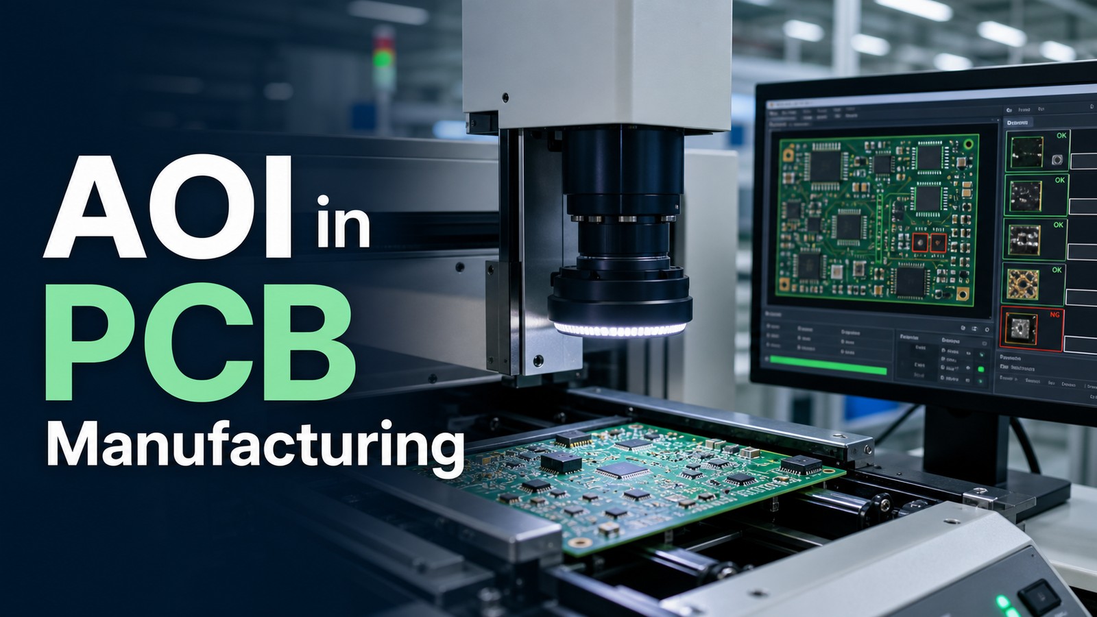
AOI in PCB manufacturing means automated optical inspection of visible board and assembly features using cameras, lighting and comparison software. It helps identify defects such as missing solder, bridging, insufficient solder, wrong component position, polarity concerns, tombstoning, scratches, contamination and other visible process issues before boards move to the next stage.
AOI is useful, but it is not a complete quality system by itself. Buyers should understand what AOI can see, what it cannot confirm, and when electrical test, X-ray, functional test or manual engineering review should be added.
AOI becomes valuable when the buyer knows what defects the inspection is expected to catch.
PCB and PCBA buyers often run into quality disputes when inspection scope is vague.
- The supplier says AOI is included, but the buyer does not know whether it covers bare board, SMT assembly or both.
- Hidden solder joints, BGA connections or internal electrical problems are expected from AOI even though optical inspection cannot see them directly.
- Design features create false calls, repeated review work or unclear acceptance decisions.
- Inspection findings are not connected back to DFM feedback, so the same defect repeats in later builds.
- The RFQ does not define test needs, sample approval, defect categories or required documentation.
EBest Circuit uses inspection planning to connect AOI findings with DFM, PCBA and production feedback.
- We review PCB and PCBA files before quoting so inspection expectations match the build scope.
- For assembly projects, we check BOM, CPL, polarity, placement risk and visible soldering concerns before production release.
- When AOI is not enough for the risk level, we help buyers define additional checks instead of relying on one inspection method.
- We use inspection feedback to support repeat production stability, not only one-time defect sorting.
AOI in PCB Manufacturing in One Practical Answer
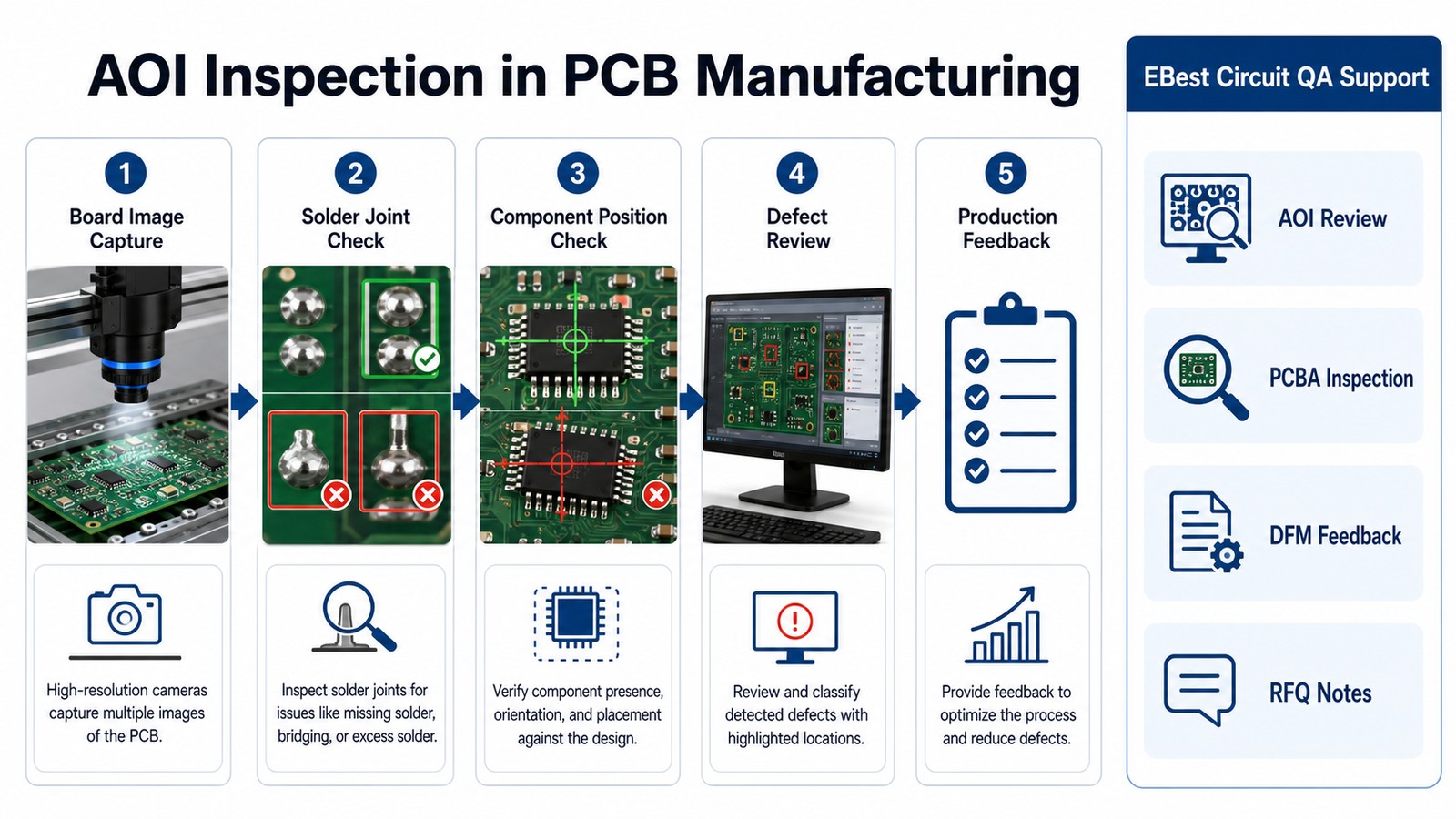
AOI is a camera-based inspection step used to detect visible PCB and PCBA defects during manufacturing. It compares board images against programmed rules, CAD data, golden samples or inspection criteria so operators can review suspected defects before the product moves forward.
Where AOI Fits in the PCB Production Flow
AOI can be used after fabrication steps and after SMT assembly, depending on the process scope. In bare-board manufacturing, it can help review visible copper, solder mask or surface issues. In PCBA, it is commonly used after solder paste, placement or reflow stages.
What AOI Can Detect on PCB Assemblies
AOI is strongest at finding visible assembly problems. Typical review items include missing parts, wrong orientation, offset placement, tombstoned components, solder bridges, insufficient solder, excess solder, lifted leads, damaged parts, contamination and polarity concerns.
| AOI Check | Typical Finding | Buyer Value |
|---|---|---|
| Solder joint review | Bridge, insufficient solder or excess solder | Reduces visible assembly escapes |
| Component check | Missing, shifted or rotated part | Supports BOM/CPL accuracy |
| Polarity review | Diode, IC or capacitor orientation concern | Prevents functional risk before power-up |
| Surface review | Scratch, stain or contamination | Supports visual acceptance decisions |
What AOI Cannot Confirm Alone
AOI cannot replace every electrical or hidden-joint test. It cannot directly prove internal connectivity, BGA solder quality under the package, intermittent electrical behavior, firmware function or long-term reliability. For hidden solder joints, X-ray or other process checks may be needed.
AOI for Bare PCB Fabrication
In bare PCB manufacturing, optical inspection helps catch visible manufacturing issues before assembly. Depending on the process and supplier setup, inspection may review surface defects, copper patterns, solder mask, silkscreen, pads, contamination or mechanical damage. For fabrication planning, see EBest Circuit’s PCB manufacturing capabilities.
Need inspection planning for a PCB or PCBA build?
Send Gerber, BOM, CPL, assembly drawings and test expectations. EBest Circuit can review whether AOI, visual inspection, X-ray or functional checks fit your project.
Gerber | BOM/CPL | PCBA | AOI | X-ray | Functional test
AOI for SMT and PCBA Builds
For PCBA, AOI should be aligned with the component package mix and soldering process. Fine-pitch ICs, polarized components, connectors, dense SMT areas and mixed-technology assemblies need clear inspection criteria. EBest Circuit’s PCBA and SMT assembly support helps buyers connect BOM/CPL data with inspection planning.
How AOI Results Should Feed Back Into DFM
AOI is most useful when repeated findings are turned into design or process feedback. If the same solder bridge, shifted component or polarity issue repeats, the next step may be pad adjustment, stencil review, placement correction, panel support or clearer assembly notes.
For file readiness before production, see the PCB design for manufacturability guide.
AOI vs X-Ray vs Functional Test
AOI checks visible defects, X-ray helps with hidden solder joints, and functional test checks whether the assembly performs its intended task. These methods answer different questions, so buyers should not treat one as a substitute for all others.
AOI Requirements Buyers Should Put in the RFQ
The RFQ should define inspection expectations before the supplier quotes the build. Include board type, quantity, assembly scope, package types, acceptance concerns, test requirements, defect priorities and whether inspection records or first-article review are needed.
Common AOI Sourcing Mistakes
The biggest mistake is asking whether the supplier has AOI without asking how inspection is used for the specific board. A useful supplier explains the inspection stage, known limits, review process and when other tests are needed.
Use EBest Circuit as your PCB inspection quote checkpoint.
A second review can help you compare DFM feedback, PCBA inspection scope, AOI limits and test planning before release.
AOI | DFM | PCBA | X-ray | Functional test | RFQ
AOI in PCB Manufacturing FAQ
What is AOI in PCB manufacturing?
AOI is automated optical inspection, a camera-based method for checking visible PCB or assembly defects during production.
Does AOI replace electrical testing?
No. AOI checks visible features. Electrical and functional tests check different risks and may still be required.
Is AOI used for bare PCB or PCBA?
It can be used in both contexts, but the inspection criteria differ. Bare PCB review focuses on visible board features, while PCBA AOI focuses on component and soldering conditions.
Can EBest Circuit support AOI planning for PCBA projects?
Yes. EBest Circuit can review Gerber, BOM, CPL, assembly drawings and test expectations to help define a practical inspection path.
Final RFQ Recommendation
Ask for AOI as part of a complete inspection plan, not as a one-word quality claim. The right supplier should explain where AOI is used, what it can detect, what needs another test and how findings feed back into production control.
Send your Gerber or ODB++, BOM, CPL, assembly drawing, quantity, inspection requirements, test expectations and target delivery plan to sales@bestpcbs.com. EBest Circuit can review AOI in PCB manufacturing requirements and provide a practical quotation path for PCB fabrication, PCBA and inspection planning.
You may also like


Tags: pcb manufacturing