EBest Circuit (Best Technology) Co.,Ltd
- +86-755-2909-1601
- sales@bestpcbs.com
|
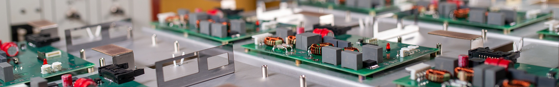
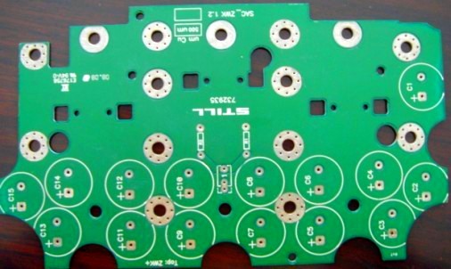
Heavy Copper Board does not have a set of definition per IPC. According to PCB industry, however, peopel generally use this name to identify a printed circuit board with copper conductors 3 oz/ft2 - 10 oz/ft2 in inner and/or outer layers. And Extreme heavy copper PCB refers to 20 oz/ft2 to 200 oz/ft2 printed circuit board. Heavy copper normally used for a various products but not limited to: high power distribution, heat dissipation, planar transformers, power convertors, and so on. |
|
Design Guide for Heavy Copper PCB |
|
Pls visit heavy copper PCB design guide for more information about design guide,or visit heavy copper PCB FAQ to make your heavy copper PCB design meet DFM better. |
|
| Capability of Heavy Copper PCB | |
|
|
| Please click here for immediate quotation online
Please contact us for more information about heavy copper PCB and extreme heavy copper printed circuit board (heavy copper PCB). |
|
ISimply drop your email or phone number in the contact form, and we'll promptly provide you with a quotation.