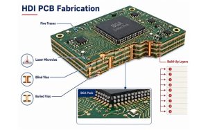
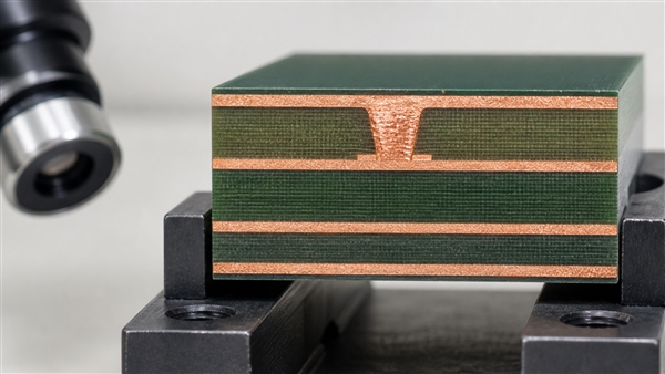
Blind vias connect an outer copper layer to an internal layer without passing through the entire PCB. Use them when dense component escape routing or an unwanted signal stub creates a problem that ordinary through vias cannot solve efficiently. They can free routing space, but add constraints to drilling, plating, stack-up and inspection. The right choice is the simplest manufacturable interconnection that meets the circuit’s needs.
What Is a Blind Via?
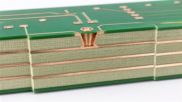
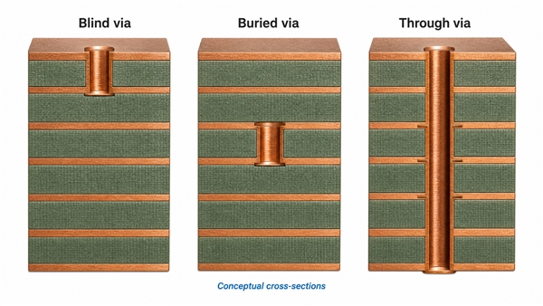
A blind via is a circuit board via with one end at an external surface and the other at an internal target layer. A blind via hole is therefore accessible from one board face but does not open onto the opposite face. For example, an L1-L2 connection in a six-layer board is blind; an L1-L6 connection is through.
For background, PCB vias are conductive connections between copper layers, not unplated mounting holes. Questions such as “what is a via?” or “what are vias?” concern this basic vias meaning; a blind via adds the condition that the connection stops inside the board.
A blind via PCB can contain other types of vias too. Using blind vias in PCB routing does not mean every connection must be blind. Through vias may remain appropriate for connectors, power distribution or signals needing a different layer span.
The construction is determined by the finished board, not only by the drilling operation. A hole drilled through a subassembly may become blind after additional layers are laminated to that subassembly.
What Is the Difference Between Blind and Buried Vias?
Blind vias and buried vias differ in whether they reach a finished board surface. A buried via connects internal layers only. Its connection must be manufactured while those layers are accessible, before they are enclosed by later lamination.
| Connection | Finished-board span | Useful when | Main trade-off |
|---|---|---|---|
| Blind via | Outer layer to internal layer | Surface component escape needs routing space below | Depth, plating and build sequence need review |
| Buried via | Internal layer to internal layer | Inner-layer routing should not consume outer pads | Hidden interconnects and additional processing |
| Through via | Entire board thickness | Conventional routing can tolerate its barrel and clearances | Unused barrel may form a stub; occupies more layers |
The buried via vs blind via decision follows the required endpoints. A buried via hole cannot directly provide the top-surface connection of a component pad. Conversely, a blind via and buried via may be combined within the same HDI stack-up. These are complementary PCB via types, not competing quality grades.
Blind Via vs Microvia: Are They Different?
Yes, but the categories overlap. “Blind” describes the layers a connection reaches. “Microvia” describes a small, shallow interconnect structure, commonly laser formed in an HDI build-up layer. A surface-to-next-layer microvia is also a blind via; a mechanically drilled blind connection is not automatically a microvia.
In a microvia PCB, several short connections can be arranged across successive build-up layers. A deeper connection should not be called a microvia merely because its opening looks small. The hole formation process, depth, diameter and applicable qualification requirements must all agree.
The practical answer to microvia vs blind via is therefore not “choose one.” First choose the required layer span, then determine whether a shallow laser microvia or another qualified blind structure can realize it.
When to Use Blind Vias?
Use blind vias when they remove a specific routing or electrical limitation. Common reasons include escaping fine-pitch BGA pads into a nearby routing layer, preserving inner-layer channels, and shortening an otherwise excessive signal-via stub.
- Dense surface routing: a short L1-L2 connection can move a signal away from a crowded pad field without reserving a through-hole clearance on every layer.
- Constrained board area: recovering routing space can help when changing the enclosure or connector locations is not practical.
- Controlled high-speed transitions: a shorter barrel may reduce the unused stub, provided the pad, antipad and return-path geometry are also suitable.
For our HDI printed circuit boards, interconnection planning starts with the component escape pattern and feasible build-up. Adding blind vias after routing is complete can force a stack-up redesign.
In compact rigid-flex circuit boards, dense connections may be needed in a rigid component area while the flexible section carries interconnects between assemblies. Any blind-via option requires construction-specific review. Do not extend a rigid-area via rule into a dynamic bend region or assume a via can sit at a rigid-flex transition without assessment.
Keep conventional through vias when they already satisfy routing, electrical and mechanical requirements. An HDI feature is not automatically an improvement on a simple board.
How Are Blind Vias Made?
The PCB blind via fabrication process depends on when the target layer is accessible. Shallow laser drilling is common for build-up microvias. Controlled-depth mechanical drilling or drilling a subassembly before further lamination can serve other blind structures.
- Define the layer pairs, materials and fabrication sequence.
- Form the hole to the intended copper target or through the relevant subassembly.
- Clean the hole and prepare the dielectric and target-pad surfaces for metallization.
- Deposit and build copper to create the electrical connection; fill and planarize when the specified construction requires it.
- Complete subsequent imaging and lamination stages, then inspect and electrically test the finished connections.
Via hole drilling is only one operation in that sequence. A correctly located cavity can still fail if residue prevents adhesion at the target pad or copper deposition is inadequate. Blind/buried vias also require clear identification of each drill span; one undifferentiated drill file cannot adequately describe several different layer pairs.
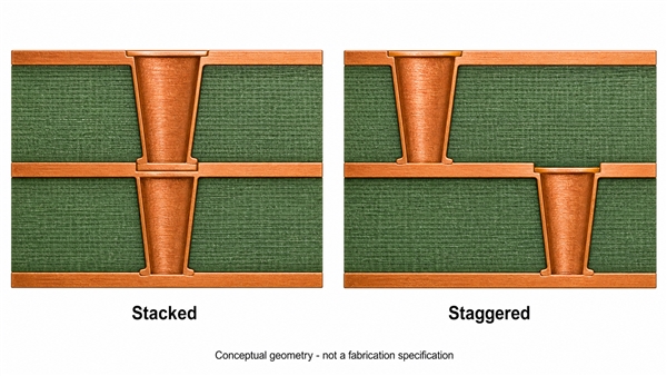
In HDI PCB design, reaching deeper routing layers may require a chain of microvias through successive build-up layers. The outer connection is blind, while connections entirely inside the finished board are buried. These successive microvias can be vertically stacked or laterally staggered, so their arrangement belongs in the fabrication plan rather than being treated as an unrelated hole type.
How Do Stacked Vias Differ from Staggered Vias?
Stacked vias align successive microvias vertically. A stacked via structure saves lateral space, but introduces copper-fill and interfacial requirements at each level. Staggered vias offset successive connections and join them with an intermediate trace or pad region.
A staggered via layout uses more area but can simplify certain interconnect interfaces. Neither arrangement is automatically reliable or unreliable: the number of build-up levels, materials, process control and qualification evidence determine suitability.
The minimum blind buried via stagger distance cannot be selected as one universal number. It depends on capture and target pad diameters, registration tolerance, copper spacing and the manufacturer’s approved construction. Measure the clearance between real copper features, not only between drill centers.
What Blind Via Aspect Ratio Is Practical?
Define the ratio before comparing limits. Here, via aspect ratio = connection depth divided by drilled hole diameter. For a blind connection, use its own depth, not the full finished-board thickness. Some supplier tables express the inverse ratio, so a bare ratio without its definition is ambiguous.
As a geometry example, an 80-micrometer-deep opening with a 100-micrometer diameter has a depth-to-diameter ratio of 0.8:1. This calculation is illustrative, not a production limit. A shallower blind via aspect ratio generally makes cleaning and copper deposition easier, but material, taper, target-pad condition and plating method still matter.
Many laser-microvia processes use shallow geometries around or below 1:1, with the acceptable value set by the qualified fabrication process. Do not apply a general through-hole aspect-ratio capability to laser microvias. A “blind via ratio” requirement must state the dimensions and convention being used.
Finished opening size, drilled diameter and bottom diameter are not interchangeable. For deeper blind structures, consult the actual process limits rather than extrapolating a shallow microvia rule.
What Changes with Blind Via in Pad Designs?
A blind via in pad can provide a short escape route directly beneath a component termination. It also puts the hole treatment and surface condition inside the soldering interface. An open cavity may consume solder or affect joint consistency.
Specify the required filling, planarization and cap treatment for the actual assembly process. A capped via has a copper-covered surface, but that name alone does not describe the complete internal fill structure or guarantee a flat solderable land. Solder-mask tenting is not the same as copper filling and capping.
For fine-pitch pads, evaluate surface depression or protrusion, finish and solder-joint requirements together. Do not assume every PCB blind vias design requires identical filling, or that any filled hole is acceptable beneath any package.
Blind Via vs Backdrill: Which Solves the Problem?
The blind via vs backdrill comparison matters when an unused plated barrel is the main concern. Backdrilling removes an unwanted portion of an already plated through via using a larger controlled-depth drill. It reduces the stub but does not create the same build-up structure as a blind microvia.
A blind connection may also free routing space below its endpoint. A backdrilled hole still needs clearance for the larger drill and a controlled residual stub. If routing space is available and the issue is primarily signal integrity, backdrilling may be worth comparing with an HDI reconstruction.
On RF printed circuit boards, the substrate and complete transition geometry must be reviewed together. A short signal barrel alone does not establish a good RF transition: return connections, pad capacitance, antipads and material behavior remain important. We assess process compatibility for the selected laminate instead of assuming every RF material supports the same blind-via process.
For backdrill vs blind via decisions, compare the modeled transition, remaining stub tolerance, routing impact and fabrication sequence. Do not promise a fixed bandwidth improvement from the via name alone.
Are Blind Vias More Expensive?
Usually, compared with an otherwise similar conventional through-via board. Blind via cost can increase because of laser or depth-controlled drilling, additional lamination stages, copper filling, registration requirements and inspection. The premium is design dependent, not a fixed percentage.
Blind vias cost should also be considered at assembly level. If the construction removes unnecessary layers or enables a substantially smaller board, the system-level result may differ from the price of one fabrication operation. Compare manufacturable alternatives with the same functional requirements.
To control cost, use only the necessary layer spans, favor a repeatable build-up, and avoid specifying maximum density throughout areas that do not need it. Simplifying a stack-up early is usually more useful than trying to negotiate around an unnecessarily complex finished layout.
Which Blind Via Design Rules Should Be Checked?
Blind via design rules for printed circuit board vias must come from the agreed stack-up and fabrication process. A printed circuit board via needs the intended copper connection and isolation from unrelated nets. A CAD rule set is useful only when its assumptions match the intended manufactured structure.
- Layer span: every via pair must have a feasible drilling and lamination sequence.
- Depth and diameter: check the stated aspect-ratio convention and the relevant hole dimensions.
- Capture and target pads: preserve registration allowance and the required copper connection.
- Clearances: inspect adjacent traces, plane antipads and the actual spacing in dense escape areas.
- Surface treatment: define fill, cap and flatness where vias share component lands.
- Return path: ensure the signal transition has an appropriate nearby reference connection.
Our PCB via size guide provides additional terminology context. Its general hole-size discussion does not replace construction-specific blind-via approval.
How Can Blind Via Reliability Be Verified?
Use complementary checks. Electrical testing detects connectivity problems; cross-section inspection examines the physical interconnect. A sample that passes continuity today may still contain an interface weakness that appears after assembly or thermal cycling.
| Verification | Purpose | Boundary |
|---|---|---|
| Stack-up and fabrication-data review | Confirm layer pairs, pad geometry and process sequence | Does not prove physical plating quality |
| Electrical testing | Identify opens and unintended shorts | Does not by itself establish fatigue life |
| Microsection examination | Inspect target-pad interface, copper distribution and fill | Samples selected locations, not every via |
| Assembly and thermal-stress qualification | Evaluate the selected construction under defined exposure | Results apply to the tested conditions and structure |
Review misregistration, contamination, copper voids, interface separation and thermomechanical stress as possible failure mechanisms. The appropriate coupon, sample plan and stress profile depend on product requirements. X-ray inspection can complement the process, but not every interface defect is visible in a conventional X-ray image.
More Questions About Blind Vias
Can a four-layer PCB use blind vias?
Yes, where an approved stack-up and process support the required layer pair. A four-layer board is not automatically an HDI board, and its layer count alone does not prove that a particular blind via is manufacturable. Compare the routing benefit with the added processing before selecting it.
Can blind vias replace thermal vias?
Not automatically. Thermal vias conduct heat toward a copper region or heat-removal path. A blind connection ending at an internal plane does not by itself carry heat to the opposite surface. Evaluate the complete thermal path, copper area and assembly rather than substituting via names.
What should be checked for Altium blind vias?
For Altium blind vias, define the stack-up and intended drill pairs, apply the fabricator-approved constraints, and inspect the exported manufacturing data. The connections displayed in the layout must correspond to actual, unambiguous layer spans in the output. This is a design review principle, not a version-specific click-by-click tutorial.
What should be checked for KiCad blind vias?
For KiCad blind vias, confirm that the selected board setup and routing rules allow the intended structure, then review the drill outputs with their start and stop layers. A rendered hole in a 3D preview does not confirm its fabrication sequence. Editor behavior and supported options depend on the version being used.
What does skip via vs blind via mean?
A skip via bypasses an intermediate conductor level to reach a deeper target. It may also be blind when it starts at an outer surface. Skipping a layer changes drilling, isolation and plating demands; it is not a way to ignore depth limits. Have the specific construction qualified instead of treating it as an ordinary adjacent-layer microvia.
Our Blind Via PCB Manufacturing Support
At EBest Circuit (Best Technology), we support blind and buried interconnection planning with our HDI manufacturing capability. Our available constructions include 1+N+1, 2+N+2 and 3+N+3 build-ups, with HDI line/space down to 2/2 mil and minimum hole capability down to 0.10 mm, subject to materials, board dimensions, stack-up and engineering review. These limits are not a blanket approval for every layer span, aspect ratio or combined feature set.
We review the proposed construction against our PCB manufacturing capabilities before treating a design as production ready. Our aim is to support the required routing and electrical function with a feasible build sequence, suitable inspection and clearly defined acceptance requirements.
Conclusion
Choose blind vias for a demonstrated routing or transition problem, not simply because the option is available. Define the endpoints, compare conventional and HDI constructions, and review depth, plating, fill and reliability together. For construction and fabrication support, contact our team at sales@bestpcbs.com.