IPC-SM-840C is the C revision of the specification for qualifying permanent solder mask used on printed circuit boards. It connects the coating’s electrical, physical and environmental performance with its intended application. For your PCB, the practical questions are which mask class applies, how the coating fits the layout, and whether it is compatible with fabrication and assembly. At EBest Circuit (Best Technology), we provide PCB manufacturing and assembly support to help turn those requirements into a buildable board.

What Is IPC-SM-840C?
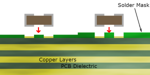
IPC-SM-840C addresses the qualification and performance of permanent polymer solder mask, also called solder resist. The coating covers selected copper and laminate surfaces while leaving soldering pads, contacts and other specified areas exposed. It helps protect conductors and define where solder should wet during assembly.
The C revision dates to January 1996, with Amendment 1 issued in June 2000. It is a historical edition, so an existing drawing may name it even when a current material datasheet names a later revision. The standard concerns both material evaluation and the way the mask is used on a board. For example, a coating qualified on a test substrate still needs a suitable application process on the actual copper pattern.
What Do IPC SM 840 Classes T and H Mean?
Class T and Class H distinguish solder mask performance requirements by end-use reliability needs. Class T covers telecommunications and other high-performance commercial or industrial equipment. Class H addresses high-reliability applications where continued operation is critical. For drawings that specify IPC-SM-840C Class T or IPC SM 840C Class H, the required designation should carry through to the selected mask material.
| Solder mask class | Application emphasis | What to specify for your board |
|---|---|---|
| IPC SM 840 Class T | Long service life in commercial and industrial electronics | Required revision, compatible mask material and intended assembly conditions |
| IPC SM 840 Class H | Higher assurance where uninterrupted operation is essential | Required revision and class, with the qualification evidence applicable to that material and process |
These letters describe the solder mask requirement. The finished PCB’s IPC-6012 Class 2 or Class 3 requirement is a separate specification covering the rigid board. Keeping both requirements explicit makes the intended coating performance and overall board quality clear.
Which Solder Mask Properties Affect PCB Reliability?
Adhesion, electrical insulation and resistance to processing exposure determine whether the coating can protect the circuit throughout manufacture and use. Colour and surface appearance matter for inspection and product presentation, but the functional properties are the basis for material selection.
| Property group | What it addresses | Relevance to the finished PCB |
|---|---|---|
| Adhesion and mechanical integrity | Bonding to the underlying surface; resistance to cracking or peeling | Maintaining coverage around tracks, pads and machined edges |
| Electrical performance | Dielectric strength and insulation resistance | Helping preserve insulation between neighbouring conductors |
| Soldering and chemical resistance | Exposure to soldering heat, fluxes and process chemicals | Keeping the mask intact through board finishing and assembly |
| Environmental performance | Moisture exposure, thermal changes and electrochemical migration | Matching the material to the board’s service conditions |
| Cure and surface condition | Developed film properties and usable surface quality | Supporting consistent handling and subsequent processing |
For our FR4 printed circuit boards, solder mask selection belongs alongside copper layout, surface finish and assembly requirements. A controller with exposed test points has different mask artwork needs from a densely populated communications board, even when both use the same laminate family.
How Does LPI Solder Mask Become a Protective Pattern?
Liquid photoimageable solder mask is applied as a coating and patterned by light exposure and development. A typical LPI soldermask process includes surface preparation, coating, preliminary drying, imaging, development and final cure. The result is a permanent film with openings matched to the circuit artwork.
Surface preparation supports adhesion; imaging and development define the openings; final cure develops the required film properties. Their combined effect explains why the material name alone is only part of the finished-board result. Dry-film photoimageable solder mask offers another material format, with different behaviour over the board’s raised copper features.
The phrase LDI vs LPI solder mask can cause confusion: LPI describes liquid photoimageable material, while laser direct imaging describes an imaging method. An appropriately formulated LPI material can be used with direct imaging. Material selection and imaging compatibility therefore need to be considered together.
What Is the Recommended Thickness for PCB Solder Masks?
The recommended finished thickness is material- and layout-specific; one universal value does not describe every PCB. Solder mask thickness affects protection over copper edges, available clearance and the local surface height around component pads. A patterned PCB is not flat: copper traces, planes and gaps create different coating conditions. Thickness over a conductor and thickness beside it may therefore differ.

An IPC SM 840 solder mask thickness requirement should identify the measurement location and the agreed finished-film requirement. A value measured over bare laminate is not directly interchangeable with one measured over copper. The material system, copper profile and circuit geometry determine the practical coating window.
This becomes especially relevant on our heavy copper PCBs: taller conductors make edge coverage and coating transitions more demanding. Providing the outer-layer copper requirement with the mask artwork allows these features to be considered together, rather than treating the mask as a uniform flat sheet.
Why Do Pad Openings and Mask Dams Matter?
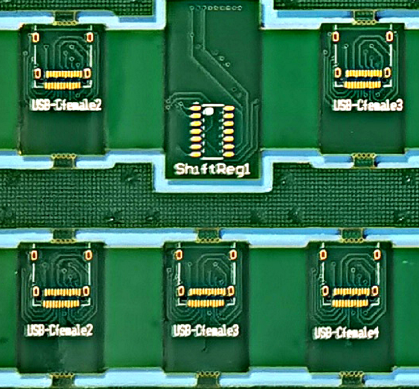
Pad openings expose the intended solderable surface, while a solder mask dam is the narrow strip of coating between adjacent openings. Registration is the alignment between the mask pattern and the copper pattern. Together, these features influence usable pad area and separation around fine-pitch components.

For our HDI boards, the pad pitch, opening size and achievable registration must work together. If a proposed dam is too narrow to manufacture consistently, the layout or opening strategy needs adjustment. The package’s land-pattern requirements remain important, particularly when choosing solder-mask-defined or non-solder-mask-defined pads.
Via tenting is a separate artwork choice: mask covers the via opening rather than filling the hole. Keep probe-access test points exposed, and specify via filling separately where that structure is required. These details help us preserve both assembly access and the intended coverage during DFM review.
How Do Surface Finish and Assembly Affect Mask Selection?
The mask must tolerate the selected board-finishing process and subsequent assembly exposure. ENIG, immersion tin and HASL use different chemical or thermal processing routes. Reflow, wave soldering and cleaning add further conditions after the bare board has been manufactured.
We offer finishes including ENIG, lead-free HASL, OSP, immersion silver and immersion tin. Sharing your intended finish and assembly route helps us discuss the appropriate board construction and mask compatibility. For a mixed SMT and through-hole assembly, the total processing sequence matters more than considering one reflow pass in isolation.
Mask colour can also affect imaging and cure settings within a material family. A green-to-black or green-to-white change is therefore a material/process choice as well as a cosmetic one. Its effect on fine features should be reviewed with the board requirements.
Solder Mask vs Conformal Coating: What Is the Difference?
Solder mask protects selected areas of the bare PCB and defines soldering openings. Conformal coating is normally applied after assembly to protect the populated board from its environment. They occupy different places in the build and can be used together.

For an industrial sensor exposed to humidity, the bare board may use solder mask while the completed assembly receives a compatible conformal coating. Connectors and test interfaces can require selective exclusion from that later coating. Adhesion between the two coatings and compatibility with cleaning residues become part of the assembly design.
Our PCB and PCBA services let you discuss bare-board manufacture and assembly as a connected project. Where additional protective coating is required, include that requirement with the assembly information so the intended materials and exposed areas are clear.
IPC SM 840 Latest Version: Is Revision C Still Current?
No. As of September 2026, the IPC document revision table lists revision E, issued in December 2010, after revision D from April 2007. C remains relevant to legacy specifications, but new project documentation should identify the edition actually required.
In the IPC SM 840 family, IPC SM 840C was followed by IPC SM 840D and IPC SM 840E. Revision E’s scope includes flexible cover materials as well as permanent solder mask. The revision letter therefore conveys technical scope, not merely a newer publication date.
If your drawing calls for C and the proposed mask documentation references E, send both with the project files. We can discuss the specified material and manufacturing route with you; any change to the drawing’s requirement should be agreed before production. The selected edition and class provide a clearer requirement than simply writing “IPC solder mask.”
How Can We Support Your PCB Solder Mask Requirements?
We combine PCB manufacturing, DFM support and assembly services, helping you match the solder mask pattern to the actual circuit. Our FR4 capability extends to 32 layers, and our HDI capability includes minimum line/space down to 2/2 mil, subject to materials, stack-up, board dimensions and engineering review. These are circuit-fabrication capabilities; the mask opening and dam requirements are reviewed separately.
For a board specified to IPC-SM-840C, send the Gerber files, fabrication drawing, required class, mask colour, surface finish and any critical pad or via details. Add assembly files when PCB assembly is part of the project. Contact our team at sales@bestpcbs.com or through our PCB manufacturing enquiry page to discuss your board.