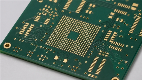
PCB surface flatness describes how closely a bare board or a defined local area conforms to its intended plane. For fabrication acceptance, bow and twist are the usual whole-board measures; for assembly, local coplanarity near a BGA, connector, thermal interface or test fixture may be just as important. At EBest Circuit (Best Technology), we control flatness through stack-up review, copper balance, lamination, panel design, routing and dimensional inspection, then align the acceptance method with your drawing and assembly process.
What Does PCB Surface Flatness Mean?
PCB flatness is not a single universal reading. A finished board can meet a bow-and-twist limit and still have a local high point that interferes with a heatsink, connector or fine-pitch package. Conversely, a small local feature may be acceptable even when a poorly supported panel appears distorted during handling. The specification must identify the object, area, condition and measurement method.
A flat surface PCB requirement should therefore answer four questions: Is the sample a production panel, a routed bare board or an assembled board? Is the concern global bow and twist or local surface profile? Is the measurement made at room temperature or through a thermal cycle? Which datum, fixture and acceptance limit apply?
Do not confuse PCB surface flatness with PCB surface roughness. Roughness describes small-scale texture, while flatness concerns form over a much larger area. PCB surface finish also affects pad planarity and solderability, but an ENIG or OSP coating cannot correct a warped laminate.
PCB Bow, Twist and Local Coplanarity: What Is the Difference?
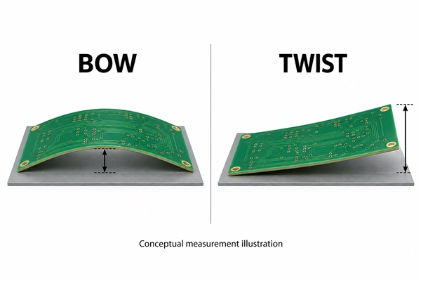
Bow is a roughly cylindrical or spherical curvature in which the corners of a rectangular board remain in one plane. Twist is diagonal deformation: three corners can touch a reference plane while the fourth is raised. Local coplanarity describes height variation within a defined region, such as a BGA land field or the mounting area for a power module.
| Condition | What changes | Useful measurement basis |
|---|---|---|
| Bow | The board curves along its length or width while the corners remain approximately coplanar | Maximum gap divided by the relevant board dimension |
| Twist | One corner rises relative to the plane formed by the other three corners | Corner displacement and diagonal length using the specified method |
| Local coplanarity | A defined pad, component or mounting region departs from its local datum plane | Profile map, CMM or optical measurement over the stated area |
| Dynamic warpage | Board shape changes as temperature changes | Thermal-profile measurement with the agreed support condition |
The phrase PCB warpage is often used broadly for bow, twist and temperature-dependent shape change. A PCB bow and twist specification is appropriate for room-temperature bare-board acceptance, but it should not be treated as proof of local BGA coplanarity or behavior during reflow.
Why Does Flatness Matter During PCB Assembly?
Assembly equipment assumes a predictable relationship between the board, stencil, placement head and support system. Excessive deformation can reduce contact between the stencil and pads, change solder-paste release, shift the focal plane for inspection, or leave a large package with uneven stand-off. Press-fit connectors, edge-card contacts and enclosure features can also become difficult to align.
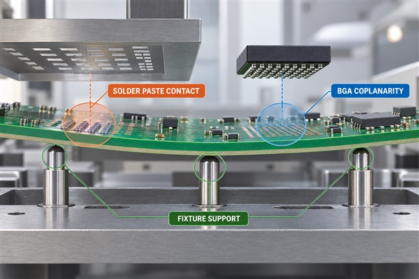
For fine-pitch assemblies, our HDI PCB manufacturing and PCB assembly services can be reviewed together. The board construction, solder-paste process, package coplanarity and underside support all affect the result. A flat bare board does not eliminate every assembly variable, and a fixture that forces a board flat can hide its free-state deformation.
Mechanical interfaces create another constraint. If a PCB must contact a thermal pad or metal baseplate, the drawing should define the mounting region and allowable gap rather than relying on a general statement such as “board must be flat.”
How Is PCB Flatness Measured?
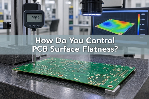
A basic PCB flatness measurement places the bare board on a precision surface plate and uses feeler gauges, a height indicator or equivalent metrology to measure the gap. IPC-TM-650 Method 2.4.22 describes production and referee procedures for bow and twist percentage on rigid boards, rigid portions of rigid-flex boards and panels. Its scope does not establish the special support conditions needed for populated assemblies.
| Measurement task | Typical equipment | Report should record |
|---|---|---|
| Go/no-go bow check | Surface plate and calculated feeler or pin gauge | Board length/width, permitted percentage and tested direction |
| Actual bow percentage | Surface plate, gauge set and dimensional measurement | Maximum gap, corresponding span and calculated result |
| Twist measurement | Surface plate, corner support and height gauge | Diagonal, raised-corner displacement and calculation method |
| Local surface profile | CMM, laser scanner or optical metrology | Datum, area of interest, point spacing and maximum deviation |
| Thermal warpage | Temperature-controlled optical measurement system | Temperature profile, support, side viewed and shape versus time |
For bow, the percentage is the maximum gap divided by the measured length or width, multiplied by 100. Under the production twist method in IPC-TM-650 2.4.22, twist percentage is the measured raised-corner gap divided by twice the diagonal, multiplied by 100. A PCB bow and twist formula must therefore match the selected procedure. A PCB bow and twist calculator is only as reliable as its inputs; using the wrong span or fixture creates a precise-looking but invalid result.
Record the board dimensions, diagonal, measured gap, test side and restraint used for every PCB bow and twist measurement. This is more useful than reporting only a pass/fail label because it makes the result reproducible.
A documented PCB surface flatness check should also identify whether protective films, tooling tabs or breakaway rails remain on the sample. If measurements from the fabricator and assembler disagree, first compare sample state, reference plane, restraint and temperature before comparing numbers.
Which Flatness Limits Should You Put on the Fabrication Drawing?
A PCB flatness specification should state the controlling document and revision, product class where applicable, maximum bow and twist, test condition, sample state and any local coplanarity zone. A PCB flatness tolerance is meaningful only when those conditions are defined. “Meet IPC” alone is incomplete because several IPC documents address different products, methods and acceptance contexts.
For our FR4 boards, we list a bow-and-twist capability of ≤0.75%, subject to the stack-up, board size, thickness, material system, copper distribution and engineering review. This is a manufacturing capability statement, not an automatic limit for every design. A thin, long board, a mixed-material stack-up or a local interface may need a different requirement and a dedicated measurement plan.
| Drawing item | Example of a clear instruction | Why it matters |
|---|---|---|
| Sample state | Routed bare board after final finish, rails removed | Prevents panel rails from masking individual-board shape |
| Global requirement | Maximum bow and twist per the named method and agreed percentage | Defines the overall acceptance calculation |
| Local requirement | Maximum plane deviation within a marked component or mounting area | Protects the interface that drives assembly performance |
| Thermal condition | Room temperature or specified temperature profile | Separates incoming inspection from reflow behavior |
| Reporting | Lot sample size, datum, instrument and measured result | Makes supplier and customer data comparable |
IPC-6012 bow and twist requirements should be interpreted with the purchase documentation and applicable revision. If your product has a tighter enclosure, optics or thermal-interface requirement, put that requirement on the drawing instead of expecting the general board class to imply it.
What Causes PCB Warpage?
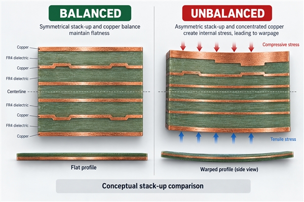
PCB warpage develops when stresses are not balanced through the board thickness or across the panel. Laminate resin, glass reinforcement, copper and surface coatings expand and contract differently. Lamination, oxide treatment, solder-mask curing, surface finishing and assembly reflow expose the construction to repeated heat and moisture changes.
- Asymmetric stack-up: different dielectric thicknesses or copper weights above and below the centerline create unequal shrinkage.
- Uneven copper distribution: a solid plane on one side and sparse routing on the opposite side can leave residual stress after cooling.
- Material mismatch: hybrid high-frequency, metal-core or stiffener constructions can respond differently to temperature.
- Thin or elongated geometry: low bending stiffness makes the same residual stress produce more visible deflection.
- Panel and routing design: weak rails, uneven coupon placement, large cutouts and an unbalanced routing sequence can release stress unevenly.
- Moisture and thermal history: storage, baking, solder-mask cure and reflow can change the free-state shape.
A PCB warpage calculation based only on laminate CTE cannot predict the final board. Copper pattern, resin flow, press cycle, panel position, routing and later assembly loads also matter. Use calculation to compare design options, then validate critical builds with representative coupons or samples.
How Do Stack-Up Symmetry and Copper Balance Reduce Warpage?
A mechanically balanced stack places similar copper weights and dielectric structures at comparable distances from the centerline. It does not require identical routing on every layer, but it avoids unnecessary imbalance in copper area and layer construction. This gives the laminate a more uniform response during pressing and cooling.
Our FR4 PCB manufacturing supports single-sided, double-sided and multilayer constructions up to 32 layers, subject to engineering review. More layers do not automatically improve or reduce flatness. What matters is the actual build: core and prepreg selection, copper weight, layer pairing, resin fill, overall thickness and panel utilization.
Copper thieving can improve local plating distribution and may help balance unused panel areas, but it is not a universal repair for an asymmetric product stack-up. We review copper distribution together with impedance, spacing and manufacturability so a flatness correction does not create an electrical or fabrication problem elsewhere.
How Do Board Thickness, Panelization and Routing Affect Flatness?
Thickness raises bending stiffness, so very thin boards are more sensitive to handling and residual stress. Our extra-thin PCB options include constructions from 0.15 mm, subject to material, size and engineering review. A thin-board requirement should therefore include panel support, assembly fixture and handling expectations rather than only the nominal thickness.
Panelization affects flatness before and after separation. Rails, crossbars, breakaway tabs, V-scores, routed slots and coupon placement change panel stiffness and the way stress is released. A large panel can pass while restrained by its frame, yet individual boards may change shape after routing. For flatness-critical parts, inspect both the production panel and the final routed board when those states serve different purposes.
Board outline matters too. Long narrow shapes, large internal windows and one-sided edge copper can create compliant regions. The best corrective action may be a stack-up change, panel rotation, added temporary support or revised routing sequence; simply increasing the final thickness can conflict with connectors, impedance or enclosure space.
Can PCB Surface Finish Improve Flatness?
A PCB surface finish can improve pad planarity relative to another finish, but it does not make the entire laminate flat. ENIG and immersion finishes deposit a comparatively uniform coating on exposed copper, while HASL can leave more variation across individual pads. This distinction matters for fine-pitch solder printing and probing.
However, the phrase PCB surface finish flat surface should not be interpreted as an overall warpage control method. Finish thickness is small compared with the board stack, and the chemical or thermal process cannot reverse a mechanically unbalanced construction. Select the finish for solderability, contact function, wire bonding, shelf life and pad-planarity needs; control global shape through the board design and fabrication process.
How Do We Control Flatness During PCB Manufacturing?
We begin with the released stack-up and panel, because most flatness risks are easier to prevent than to sort after fabrication. Our DFM review looks for asymmetry, concentrated copper, thin long geometry, mixed materials, large openings, unusual routing and local interfaces that deserve their own tolerance.
- Confirm the applicable flatness definition, acceptance method and sample state.
- Review layer symmetry, dielectric distribution and copper balance.
- Plan panel rails, coupons, scoring or routing so the panel remains stable during processing.
- Control lamination, curing and cooling according to the approved material and stack-up.
- Inspect at the state that matters: panel, routed bare board and, when separately agreed, the assembly condition.
- Use dimensional data to distinguish a design-driven pattern from a process or handling issue.
Our listed quality capabilities include 3D dimensional measurement, AOI, microsection analysis and electrical testing. These tools answer different questions. Flatness metrology measures shape; electrical testing checks continuity and insulation; microsectioning examines internal structure. One result should not be presented as proof of another.
What Should You Check After Reflow or Depaneling?
A room-temperature bare-board check is not the same as an assembled-board assessment. During reflow, the board becomes less stiff and materials expand at different rates. Components, solder, edge supports and fixtures add loads that are outside the basic bare-board bow-and-twist method. After cooling, some deformation recovers and some may remain.
When failure appears only after assembly, compare incoming flatness, panel location, paste printing, reflow profile, support-pin layout, component distribution and depaneling method. Measure the board both free and in its intended fixture if the product relies on mounting force. Record which condition produces the functional problem.
For a connector or thermal interface, inspect the actual local zone rather than averaging the entire board. For BGA-related opens, separate PCB shape from package warpage, paste volume and pad design before changing the fabrication limit.
What Information Should You Send for a Flatness-Critical PCB Order?
Send the fabrication files and a controlled drawing that identifies the critical flatness requirement. A complete manufacturing package includes:
- Finished board dimensions, outline and panel preference
- Layer count, proposed stack-up, copper weights and finished thickness
- Material system and any mixed-material or stiffener construction
- Maximum bow and twist, controlling method and sample state
- Local coplanarity area, datum, maximum deviation and inspection method
- Assembly process, peak thermal exposure and fixture constraints
- Critical components, connectors, heat spreaders and enclosure interfaces
- Required report format, sample size and lot traceability
At EBest Circuit (Best Technology), we will review the requirement against the actual board construction instead of treating one percentage as universal. Send your files and target PCB surface flatness criteria to sales@bestpcbs.com. We can align the drawing, manufacturing plan and assembly risk before production planning.