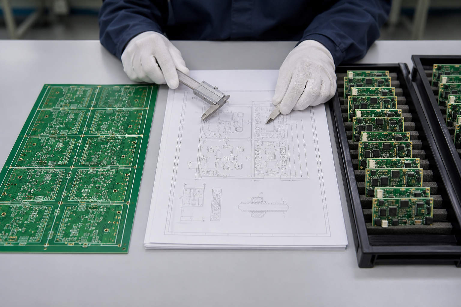
A PCB panelization drawing is not just a convenient way to place several boards on one manufacturing panel. It defines how the boards will be fabricated, handled, assembled, separated, counted and delivered. If those decisions are left unclear, a technically correct PCB can still require a new quotation, a revised fixture, manual handling or a last-minute production change.
The practical goal is simple: approve the panel before it becomes a production constraint. This guide helps PCB engineers and buyers decide who should create the array, what the manufacturer needs to review, and which details must be frozen before fabrication and assembly begin.
What Should Be Confirmed Before PCB Panelization?
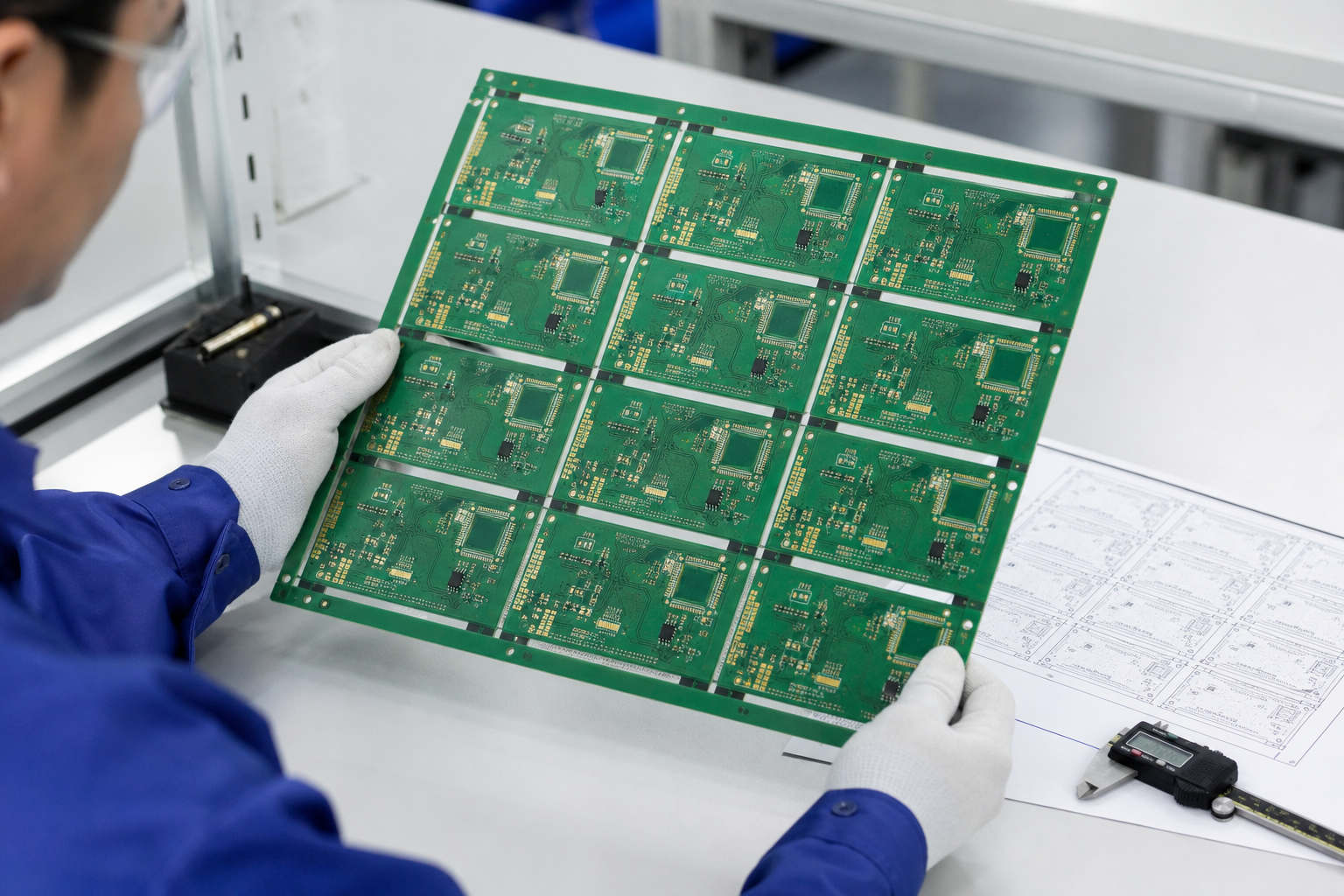
Panelization should begin with the required production and delivery flow—not with a target number of boards per panel. Before a panel drawing is created, confirm the following points.
- Required delivery unit: Will the supplier deliver individual PCBs, complete panels or assembled boards separated after SMT?
- Single-design or mixed panel: Will every position contain the same design, or must several part numbers share one panel?
- Quantity basis: Is the order and quotation based on individual pieces or complete panels?
- Downstream process: Will the panel pass through solder paste printing, pick-and-place, reflow, AOI, functional testing or another fixture-dependent process?
- Allowed panel changes: May the fabricator rotate boards, change the up count or adjust the rails to improve manufacturability?
- Depaneling responsibility: Will separation occur at the PCB factory, PCBA factory or customer site?
- Quality rules: Are X-outs allowed? Are panel-level traceability, coupons, electrical testing or special packaging required?
These answers create the design boundary. Without them, two suppliers can interpret the same Gerber package differently and return quotations that do not cover the same deliverable.
The board construction also matters. A standard FR4 PCB may allow several practical layouts, while a thin flexible circuit, brittle ceramic substrate, heavy-copper board or impedance-controlled multilayer design can impose additional handling and process limits.
Who Should Control the Panelization Design?
Who should control the layout depends on the equipment and downstream processes the panel must fit.
Let the PCB manufacturer create the panel when:
- You are supplying a single-board Gerber package.
- The main objective is manufacturability and material utilization.
- No customer-owned pallet, stencil or assembly fixture fixes the panel dimensions.
- The manufacturer may adjust rails, spacing and orientation within agreed limits.
In this situation, send the finished board data and the required delivery conditions. The fabricator can propose a production panel based on its process and working-panel format. You should still review the production drawing before release.
Supply or control the array when:
- A stencil, carrier, test fixture or automated line already depends on a fixed outline.
- Several different boards must be delivered as one matched set.
- Board orientation is controlled by a connector, sensor, coating or assembly requirement.
- The panel must match an approved repeat-order configuration.
- Traceability or packaging is managed at panel level.
The safest handoff is a documented division of responsibility. The customer defines the functional and downstream constraints, while the manufacturer confirms that the proposed panel can be fabricated, assembled and separated without creating avoidable risk.
Do not assume that an old panel should automatically be reused. A change in laminate, copper weight, board thickness, component placement, assembly site or delivery format can make the previous array unsuitable even when the circuit revision appears minor.
How Should PCB Panelization Methods Match the Board?
The best separation method is the one that fits the board outline, component layout, material and downstream handling—not simply the least expensive cutting process.
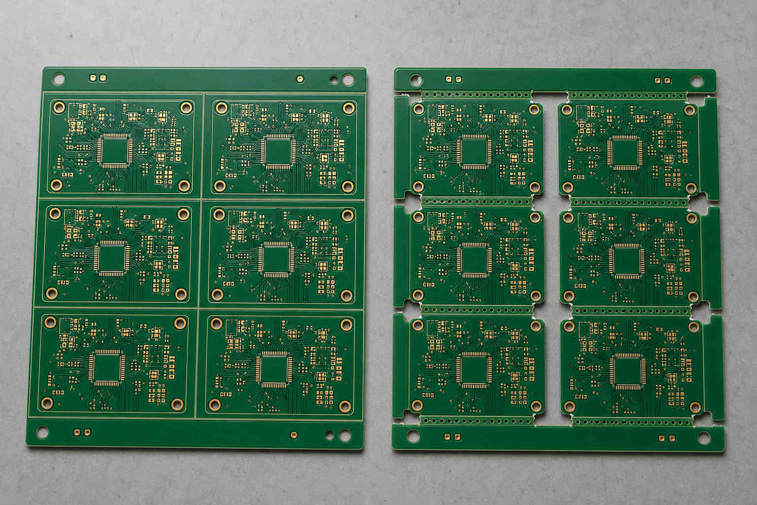
- V-scoring is usually considered when boards have straight shared edges and can be arranged in rows. It can support efficient separation, but the score line and remaining web must be reviewed against board thickness, copper distribution and nearby components. Components, solder joints and brittle features should not be placed where bending during separation can transfer damaging stress.
- Tab routing is useful for irregular outlines or layouts that cannot share continuous straight edges. Routed gaps define most of the finished profile, while tabs keep each board connected to the array. Tab position, width and removal method should be agreed before production. Poorly positioned tabs can leave difficult edge cleanup or transfer force toward sensitive areas.
- Mouse-bite perforations can make manually removed tabs easier to break, but hole size, pitch and distance from the finished edge affect the remaining witness marks. If the enclosure requires a smooth edge, secondary finishing or a different tab strategy may be needed.
- Mixed-design panels may reduce handling for matched products, but they require additional control. The designs must be compatible in material, thickness, copper build, surface finish, process route and delivery quantity. Combining unrelated boards only to fill open space can complicate fabrication, assembly and quality disposition.
Special constructions require more than a generic rectangular array:
- A rigid flex PCB may need temporary support and careful control of the flexible areas.
- A ceramic PCB is brittle, so separation force and edge damage need particular attention.
- Heavy-copper and asymmetrical multilayer boards may require warpage review.
- Thin boards and FPCs may depend on tooling or carriers for stable assembly handling.
- Impedance-controlled boards require the approved stackup and coupon strategy to remain aligned with the production panel.
This is why PCB panelization methods should be selected after the manufacturer reviews the actual build—not copied from a visually similar board.
How Do PCB Panel Size and Array Quantity Affect Cost?
More boards per panel do not automatically mean a lower total cost. The better question is whether the selected PCB panel size creates a stable, repeatable route through fabrication and assembly.
The real panel cost is influenced by:
- The usable manufacturing area and required process margin.
- Board outline, rotation and spacing.
- Rail width and routing channels.
- Tooling holes, fiducials, coupons and identification areas.
- Material type, copper weight, layer count and stackup.
- Fabrication yield and the policy for defective units within a panel.
- SMT line limits, stencil dimensions and fixture size.
- Whether the supplier ships by piece or by complete panel.
For example, increasing an array from four boards to six may improve laminate utilization, but it can also make the panel less rigid, exceed an assembly-line limit or increase the commercial impact of one rejected panel. Conversely, an array with generous unused space may be justified when it provides the rails, support and keep-outs required for stable processing.
Buyers should request a quotation that states:
- Finished board size.
- Proposed panel size.
- Number of boards per panel.
- Number of panels and total good-board quantity.
- Whether X-outs are permitted.
- Whether the price includes depaneling.
- Whether assembly and final delivery are quoted per panel or per finished board.
This removes a common source of price confusion: two quotations may show the same piece quantity while assuming different panel counts, separation work or acceptable panel yield.
How Should Panel Design Support Assembly and Depaneling?
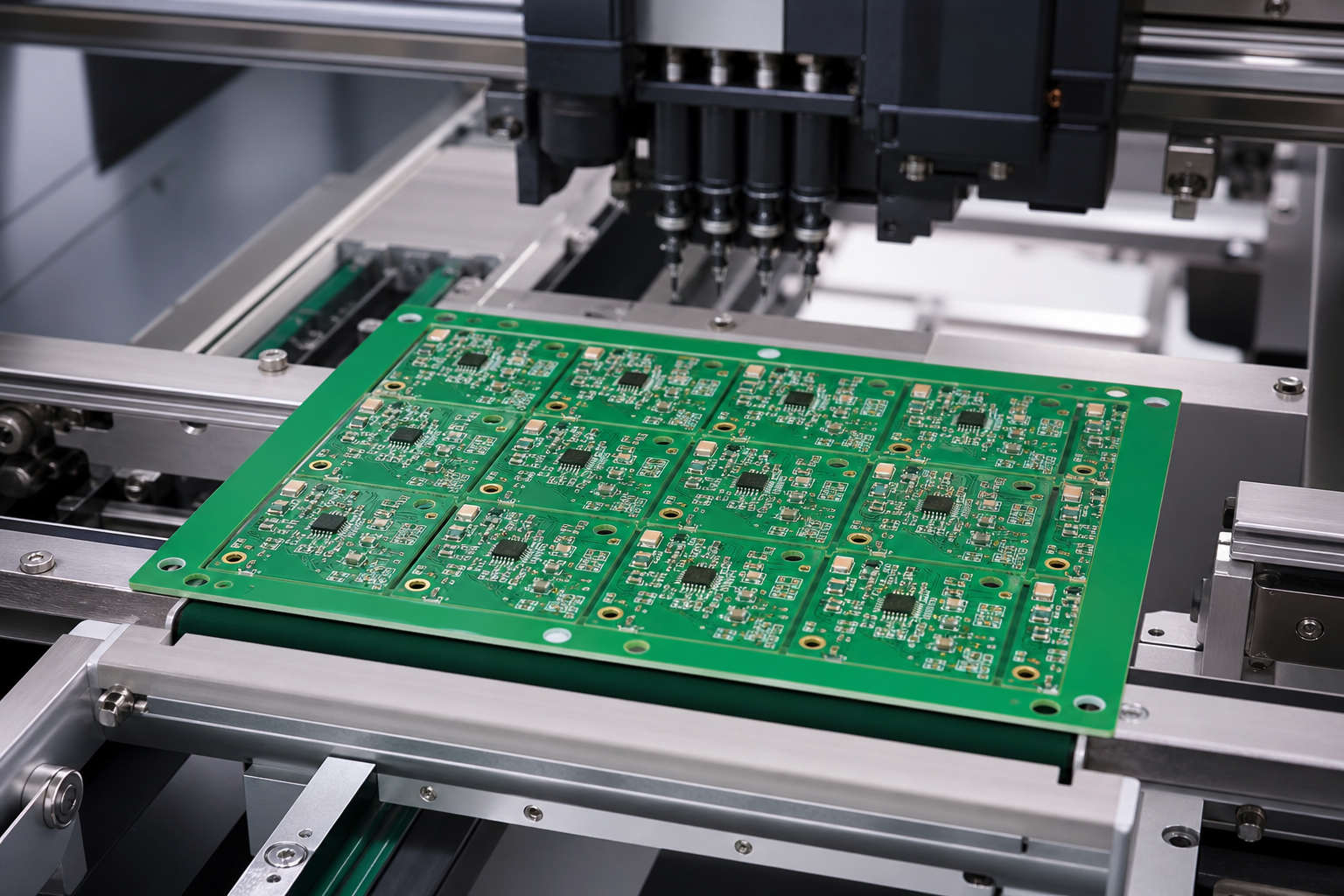
A fabrication-efficient array can still be inconvenient for PCBA. The panel should be reviewed as a temporary production tool that must remain stable from solder paste printing through final separation.
For automated assembly, check:
- Rails provide sufficient support for conveyors and board handling.
- Global fiducials and tooling holes match the assembler’s requirements.
- Component orientation supports the intended process flow.
- Edge components, connectors and overhanging parts have enough clearance.
- The panel remains sufficiently rigid through printing, placement and reflow.
- Barcode, serial-number and traceability locations remain accessible.
- Test points and fixtures can reach the required locations.
For depaneling, check:
- Score lines or tabs do not intersect copper, plated features or sensitive areas.
- Tall, heavy, ceramic or brittle components are kept away from high-stress separation zones.
- The selected tool can access every separation path.
- Edge quality is suitable for the enclosure or mechanical interface.
- The separated board can be handled and packaged without damaging protruding parts.
If one supplier handles both PCB fabrication and prototype PCB assembly, the panel can be reviewed against the real SMT flow before the first build. The customer retains final approval, while the combined review reduces handoff gaps between a fabrication-only drawing and the assembly process that follows.
What Should Be Reviewed Before Production Approval?
The production panel drawing should turn assumptions into visible, reviewable requirements. Before approval, compare it with the released board files, assembly information and purchase requirements.
Review at least these items:
- Revision identity: Board part number, revision and file date match the released package.
- Finished outline: Board dimensions, slots, cutouts and critical tolerances are correct.
- Array definition: Panel dimensions, up count, orientation and mixed-board arrangement are identified.
- Separation features: V-scores, routed gaps, tabs and mouse bites are dimensioned and correctly located.
- Manufacturing rails: Rail width, tooling holes, fiducials, coupons and markings are included where required.
- Component clearance: Assembly keep-outs and edge-component risks have been checked.
- Stackup and material: Thickness, laminate, copper build and impedance requirements match the approved construction.
- Quality disposition: X-out rules, test requirements and acceptance criteria are recorded.
- Delivery format: Panel delivery, individual-board delivery or post-assembly separation is stated.
- Packaging and traceability: Panel quantity per package, labels, date codes and protective packaging are defined.
Record technical questions and answers in a controlled engineering-query log. If the fabricator changes the up count, orientation, score position, tooling rail or stackup, the revised drawing should be approved before production rather than accepted through an informal message.
For repeat orders, confirm that the approved panel revision still matches the current PCB, BOM, assembly drawing and delivery requirement. A previously manufactured panel is useful evidence, but it is not a substitute for revision control.
PCB Panelization Case Study: From Panel Approval to Assembly
A two-layer PCB project shows why panel approval must cover fabrication, assembly and final delivery—not just the number of boards in an array.
The project used a two-layer PCB with 370HR material, 1.5 oz copper, a finished thickness of 1.57 mm with tolerance, ENIG and IPC Class 3 requirements. The fabrication record also specified plugged vias, identification markings and electrical testing.
The important panelization decision was not simply how many boards could fit on a working panel. The documented production flow required:
- The blank-board manufacturer to create the production panel.
- The production panel drawing and stackup to be sent for customer confirmation.
- Bare PCBs to be electrically tested before assembly.
- Bare boards to be delivered in panel form for lead-free SMT.
- Finished assemblies to be separated and delivered as individual boards.
- Final assembled boards to use antistatic packaging.
This sequence created three different definitions that had to remain consistent: the individual PCB design, the fabrication panel and the post-SMT delivery unit. If the quotation had stated only the number of individual boards, it would not have fully described the required work.
The approval review therefore needed to verify the panel outline, rails, fiducials, tooling provisions, up count, stackup, assembly handling and final separation responsibility. The value came from connecting fabrication data with assembly and delivery requirements before production began, instead of treating panelization as an isolated CAM step.
For buyers, the practical lesson is to approve the full route—not only the Gerber image. A panel is temporary, but the decisions built into it affect every board passing through the line.
FAQs About PCB Panelization
Should I include a panelized Gerber file when requesting a quotation?
You may provide one when a fixed array is required, but also include the single-board Gerber data and clearly identify which file controls production. If no fixture or downstream constraint fixes the array, sending the single-board data plus your delivery requirements allows the manufacturer to propose a manufacturable panel.
Can a PCB manufacturer change my panelization design?
The manufacturer may recommend changes to spacing, rails, tooling features, orientation or separation details. No production-affecting change should be assumed automatically. The proposed production drawing and any engineering questions should be reviewed and approved through revision control.
Is V-scoring always cheaper than tab routing?
Not in every project. V-scoring can be efficient for boards with compatible straight edges, while routed tabs suit many irregular outlines. The total cost also depends on material utilization, routing time, assembly handling, edge-quality requirements and the selected depaneling process.
Can different PCB designs be placed on the same panel?
Yes, when the designs and manufacturing routes are compatible. Material, thickness, copper build, surface finish, process steps, assembly requirements and quantities must be reviewed together. A mixed panel should solve a production or delivery need, not merely fill unused space.
What files are needed for a panelization review?
Send the released single-board Gerber or ODB++ package, NC drill data, fabrication drawing, stackup and impedance requirements. For assembled products, also send the BOM, centroid or pick-and-place file, assembly drawings, component height information, required delivery format and any stencil, pallet, fixture or test constraints.
Before approving your next panel, send EBest Circuit (Best Technology) the released PCB files, assembly requirements and intended delivery format. You work with one dedicated sales contact backed by three engineers, giving you one communication channel for manufacturability review, PCB fabrication, component sourcing and PCBA assembly. For a panelization and DFM review, contact sales@bestpcbs.com.
Confirm the PCB panelization route before production so the quotation, fabrication panel, SMT process and final delivery unit describe the same product.