PCB manufacturing PCB manufacturing
Home > Blog

Rogers RT/duroid 5880 PCB: Dk, Loss Tangent, Thickness & Price Guide

August 18th, 2026

A Rogers RT/duroid 5880 PCB uses a low-loss, glass-microfiber-reinforced PTFE laminate for RF and microwave circuits. Its low dielectric constant and dissipation factor support transmission lines, antennas, radar circuits, and RF feed networks where insertion loss, impedance, or phase stability must be controlled.

That does not mean every wireless PCB needs RT/duroid 5880. For short RF traces or less demanding frequencies, FR4 or another RF laminate may offer a better cost-performance balance. The useful question is whether the electrical benefit of RT/duroid 5880 solves a real design constraint.

At EBest Circuit, we support Rogers RT/duroid 5880 PCB prototypes and production builds with stackup review and controlled-impedance fabrication. Send your Gerber or ODB++ files, stackup, impedance requirements, quantity, and test notes to sales@bestpcbs.com for engineering review.

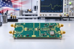
Rogers RT/duroid 5880 PCB low-loss RF material guide illustration

What Is Rogers RT/duroid 5880 PCB?

A Rogers RT/duroid 5880 PCB uses RT/duroid 5880 laminate as part or all of its dielectric structure. Rogers describes the material as a PTFE composite reinforced with randomly oriented glass microfibers.

Unlike standard FR4, the dielectric in an RF PCB is part of the electrical system. Its Dk, thickness, loss tangent, and copper interface affect transmission-line behavior.

RT/duroid 5880 is therefore most useful when the design needs:

  • low dielectric loss over RF or microwave signal paths;
  • predictable microstrip or stripline impedance;
  • phase consistency between RF channels;
  • a low-Dk substrate for antenna or transmission-line geometry;
  • repeatable high-frequency electrical behavior.

For a simple wireless control board with only a short antenna feed, this performance may be unnecessary. For a microwave network or phase-sensitive antenna circuit, the material can directly affect the finished RF response.

What Are the Key Rogers RT/duroid 5880 Datasheet Specifications?

The Rogers RT duroid 5880 datasheet values below are the properties most relevant to PCB design, stackup planning, and fabrication.

For a broader material-selection framework, see our PCB material guide.

Property RT/duroid 5880 Typical Value Why It Matters
Material Glass-microfiber-reinforced PTFE Determines RF and processing behavior
Process Dk 2.20 ± 0.02 Indicates dielectric consistency
Design Dk 2.20 Used for circuit design and modeling
Dissipation factor 0.0009 at 10 GHz Affects dielectric insertion loss
Moisture absorption 0.02% Relevant to environmental stability
Thermal conductivity 0.20 W/m·K Useful for thermal review
CTE X / Y / Z 31 / 48 / 237 ppm/°C Important for mechanical and via reliability
Density 2.2 g/cm³ Relevant to mechanical design
Copper peel strength 5.5 N/mm Indicates copper adhesion performance
Flammability UL94 V-0 Material flammability classification

These are published laminate values, not automatic tolerances for a finished PCB. A fabrication drawing should separately define the requirements that need production control, such as dielectric thickness, copper weight, finished thickness, impedance, and dimensional tolerances.

RT/duroid 5880 specifications and common dielectric thicknesses

What Is the Dielectric Constant of Rogers RT/duroid 5880?

The published Rogers RT duroid 5880 dielectric constant is 2.20 ± 0.02 for process Dk, with a design Dk of 2.20.

For an RF designer, Dk affects more than impedance. It also influences:

  • signal propagation velocity;
  • wavelength inside the PCB;
  • microstrip and stripline dimensions;
  • resonator dimensions;
  • antenna geometry;
  • electrical phase length.

If dielectric thickness or Dk changes after layout is completed, a transmission line may no longer meet its original impedance or phase target.

This is why a 50 Ω note on a drawing is not enough for a high-frequency board. The manufacturer should also know the intended laminate thickness, copper thickness, RF structure, and impedance tolerance.

For sensitive microwave circuits, prototype validation is useful even when the nominal Dk is known. Actual performance still reflects the complete transmission structure rather than one datasheet number.

What Is the Loss Tangent of Rogers RT/duroid 5880?

The published Rogers RT duroid 5880 loss tangent, or dissipation factor, is 0.0009 at 10 GHz.

A low Df reduces the dielectric contribution to transmission loss. That becomes more valuable as frequency increases, RF routes become longer, or a design contains multiple cascaded transmission structures.

Typical examples include:

  • microwave feed networks;
  • RF filters and couplers;
  • long antenna feed lines;
  • radar channels;
  • phase-sensitive RF networks.

Low Df does not eliminate every source of loss. Copper profile, line geometry, connectors, launches, vias, surface finish, and discontinuities still contribute to the total insertion-loss budget.

In practice, there is little value in specifying a very low-loss laminate while leaving the RF stackup or transition geometry poorly controlled.

What Thicknesses Are Available for Rogers RT/duroid 5880 PCB?

Common Rogers RT duroid 5880 thickness options include:

Nominal Thickness Metric Equivalent
0.005 in 0.127 mm
0.010 in 0.254 mm
0.020 in 0.508 mm
0.031 in 0.787 mm
0.062 in 1.575 mm

These figures refer to the dielectric laminate thickness, not necessarily the finished PCB thickness. Copper foil, plating, bonding layers, solder mask, and multilayer construction all affect final board thickness.

Thickness also changes RF geometry. For the same impedance target, a different dielectric height usually requires a different trace width.

Before releasing RF artwork, confirm:

  • laminate thickness;
  • copper thickness;
  • impedance target and tolerance;
  • intended transmission-line structure;
  • manufacturable trace width.

Changing one of these after the layout is frozen can force the RF traces to be redesigned.

Why Is RT/duroid 5880 Used for High-Frequency PCB Designs?

RT/duroid 5880 is attractive when the circuit needs low dielectric loss and predictable RF behavior.

Its main engineering advantages are straightforward:

  • Low Dk: supports specific transmission-line and antenna geometries.
  • Low Df: reduces dielectric loss at microwave frequencies.
  • Good dielectric consistency: useful for impedance and phase-sensitive layouts.
  • Low moisture absorption: helps limit electrical changes caused by humidity.
  • PTFE-based construction: suited to demanding microwave and broadband circuits.

There is also a practical limit.

If a circuit has short RF paths, relaxed loss requirements, and strong cost pressure, another laminate may be sufficient. RT/duroid 5880 should solve a measurable RF problem rather than simply make the material specification look more advanced.

Where Is Rogers 5880 PCB Commonly Used?

RT/duroid 5880 is commonly associated with RF and microwave circuits where the transmission structure is sensitive to dielectric loss or Dk variation.

Typical applications include:

  • microwave antenna feed boards;
  • phased-array antenna networks;
  • radar front-end circuits;
  • point-to-point wireless links;
  • satellite communication modules;
  • microwave filters and couplers;
  • RF test and measurement fixtures;
  • aerospace RF assemblies;
  • low-loss microstrip and stripline circuits.

The application name alone should not determine material choice. A short 2.4 GHz antenna trace inside a commercial product has very different requirements from a multi-channel microwave array where small phase errors accumulate across many RF paths.

A useful selection question is: what performance parameter becomes unacceptable if a lower-cost laminate is used?

If there is no clear answer, RT/duroid 5880 may be over-specified.

Typical Rogers RT/duroid 5880 PCB applications including radar antennas and satellite communication

Rogers RT/duroid 5880 vs 5880LZ vs 5870: Which Should You Choose?

These materials belong to the RT/duroid family, but they are not interchangeable.

Property RT/duroid 5880 RT/duroid 5880LZ RT/duroid 5870
Process Dk 2.20 ± 0.02 2.00 ± 0.04 2.33 ± 0.02
Design Dk 2.20 2.00 2.33
Df at 10 GHz 0.0009 0.0021 0.0012
Density 2.2 g/cm³ 1.4 g/cm³ 2.2 g/cm³
Main Selection Driver Very low dielectric loss Low density and low Dk Low-loss PTFE with higher Dk

Choose RT/duroid 5880 when very low dielectric loss and a Dk around 2.20 suit the RF design.

Choose 5880LZ when lower weight is a major mechanical requirement. Its lower density can be useful in weight-sensitive aerospace and antenna applications.

Choose 5870 when its 2.33 Dk fits the RF geometry or when an existing design is already qualified around that material.

Do not substitute one for another without recalculating the RF structure. A Dk change can alter impedance, resonant dimensions, and electrical length.

What Design Rules Matter for Rogers RT/duroid 5880 PCB?

The first rule is to design around the real manufacturing stackup, not a generic “Rogers 5880” material label.

Our PCB board stackup guide explains how copper and dielectric layers work together before routing is finalized.

For line-structure tradeoffs, compare the routing guidance in our stripline vs microstrip guide.

For controlled RF lines, review these items together:

  • dielectric height;
  • trace width;
  • copper thickness;
  • copper type or profile;
  • reference-plane position;
  • surrounding dielectric structure;
  • impedance tolerance.

RF via transitions also deserve attention. A signal via with nearby ground vias behaves differently from an ordinary low-frequency interconnect. At higher frequencies, launch geometry, anti-pad size, return-current path, and via stub length can affect performance.

For phase-matched channels, equal CAD length alone is not enough. The dielectric environment and transitions along each path should remain as similar as practical.

It is also useful to confirm material availability before freezing the layout. If the final production dielectric thickness differs from the value used in simulation, controlled-impedance traces may need to be resized.

What Should Be Controlled During RT/duroid 5880 PCB Fabrication?

RT/duroid 5880 is a PTFE-based material, so it cannot simply be processed as if it were standard FR4.

The main fabrication controls are:

Process Key Control
Material handling Prevent scratches, dents, contamination, and distortion
Surface preparation Avoid aggressive abrasion on soft PTFE laminate
Drilling Control drill condition, feed, speed, stack height, and tool life
Hole-wall treatment Prepare PTFE surfaces correctly before metallization
Plating Maintain reliable adhesion and hole-wall coverage
Etching Control finished RF trace width
Routing Support the softer laminate during machining
Lamination Match bonding system and press process to the stackup
Inspection Verify dimensions, continuity, impedance, and critical RF geometry

Drilling and hole-wall treatment deserve particular attention because PTFE behaves differently from epoxy-glass material. Poor processing can create smear, plating adhesion problems, or dimensional issues around drilled features.

Etching accuracy matters as well. A trace that is electrically critical should be controlled according to its finished width, not merely the CAD artwork dimension.

For prototype projects, we can review the proposed stackup, copper specification, via construction, impedance requirement, and mechanical features before fabrication. This is especially useful when an RF simulation moves into its first physical build.

Rogers RT/duroid 5880 PCB design and fabrication control illustration

What Affects Rogers RT/duroid 5880 PCB Price?

There is no useful universal Rogers RT/duroid 5880 PCB price because laminate cost is only one part of the finished board.

The main quotation variables are:

  • Laminate thickness: uncommon constructions may cost more or take longer to source.
  • Copper type and weight: rolled copper, ED copper, and different copper weights affect material cost.
  • Board size and panel utilization: irregular shapes can waste expensive laminate.
  • Layer count: multilayer and hybrid boards require additional lamination and registration control.
  • Impedance tolerance: tighter limits may require coupons and additional verification.
  • Hole structure: dense PTH patterns, small holes, cavities, or slots increase process complexity.
  • Mechanical tolerances: tighter dimensions can reduce yield.
  • Quantity: prototype setup costs are spread across fewer boards.
  • Testing: impedance measurement, electrical test, and extra inspection add cost.

A cheaper quotation is only meaningful when both suppliers are pricing the same construction.

Before comparing prices, check that the quoted material, dielectric thickness, copper weight, finished thickness, impedance tolerance, test scope, and quantity are identical.

What Information Is Needed for a Rogers RT/duroid 5880 PCB Quote?

A complete RFQ saves time and reduces assumptions during stackup review.

For an accurate quotation, provide:

  • Gerber, ODB++, or equivalent manufacturing files;
  • fabrication drawing;
  • board dimensions;
  • layer count;
  • RT/duroid material designation;
  • dielectric thickness or proposed stackup;
  • finished PCB thickness;
  • copper type and weight;
  • controlled-impedance targets and tolerance;
  • minimum finished hole size;
  • surface finish;
  • special routing, slot, cavity, or edge-plating requirements;
  • testing requirements;
  • prototype and production quantities.

If the stackup has not been finalized, state that clearly. The manufacturer can then propose a practical construction before the RF layout is locked.

A request such as “4-layer Rogers 5880 PCB, 50 Ω” leaves several important variables unresolved. Adding dielectric spacing, copper weight, RF layer location, impedance tolerance, board size, and quantity makes both engineering review and quotation much more reliable.

Rogers RT/duroid 5880 PCB price factors and RFQ checklist

FAQs About Rogers RT/duroid 5880 PCB

Is Rogers RT/duroid 5880 a PTFE material?

Yes. RT/duroid 5880 is a glass-microfiber-reinforced PTFE laminate designed for high-frequency circuits. Its construction is different from standard FR4 epoxy-glass material.

Is Rogers 5880 suitable for millimeter-wave PCB designs?

It can be used for millimeter-wave designs where its low dielectric loss and Dk characteristics suit the circuit. At these frequencies, however, copper profile, connector launches, vias, line geometry, and fabrication tolerance also become critical.

Can RT/duroid 5880 be used in multilayer or hybrid PCBs?

Yes. It can be used as selected RF layers in multilayer or hybrid constructions. The bonding system and adjacent dielectric materials should be included in the RF stackup model where they influence the transmission structure.

Hybrid construction can also reduce the amount of premium RF laminate used when only part of the PCB requires very low dielectric loss.

What Is the Difference Between Rogers 5880 and FR4?

RT/duroid 5880 is a PTFE-based high-frequency laminate with a design Dk of 2.20 and a published Df of 0.0009 at 10 GHz. FR4 is an epoxy-glass material family designed for much broader general-purpose PCB use.

FR4 usually provides a lower-cost manufacturing route. RT/duroid 5880 becomes attractive when low RF loss, stable dielectric behavior, or specific high-frequency geometry justifies its higher material and processing cost.

Is RT/duroid 5880 the Same as 5880LZ?

No. RT/duroid 5880 and 5880LZ are separate materials.

5880 has a design Dk of 2.20 and Df of 0.0009 at 10 GHz. 5880LZ has a lower Dk and substantially lower density, making it useful when board weight is an important design constraint.

They should not be substituted without reviewing impedance, electrical length, antenna geometry, and mechanical requirements.

How Can EBest Circuit Support Your Rogers RT/duroid 5880 PCB Project?

Rogers RT/duroid 5880 makes sense when its low dielectric loss and 2.20 Dk solve a genuine RF problem. The laminate is only part of the result; dielectric thickness, copper, line geometry, drilling, PTFE processing, lamination, and impedance control all influence the finished PCB.

At EBest Circuit, we support high-frequency PCB stackup review, controlled-impedance fabrication, prototypes, and production. Send us your Gerber or ODB++ files, target stackup, RT/duroid 5880 thickness and tolerance, copper specification, impedance targets, surface finish, quantity, and test requirements for engineering review and quotation.

You may also like

Rogers PCB: Materials, FR4 Comparison, Fabrication & Cost Guide

August 18th, 2026

A Rogers PCB is usually considered when standard FR4 can no longer meet the electrical requirements of an RF, microwave, antenna, radar, or other frequency-sensitive circuit. Compared with general-purpose FR4, Rogers laminates such as RO4003C, RO4350B and RT/duroid 5880 offer lower dielectric loss and more tightly controlled dielectric properties for high-frequency designs.

EBest Circuit is a PCB and PCBA manufacturer with over 20 years of experience, with manufacturing facilities in China and Vietnam. We support Rogers PCB fabrication, Rogers/FR4 hybrid boards, controlled-impedance PCBs, and PCB assembly for high-frequency projects. Our RF PCBs are used in microwave systems, radar, IoT communication, wireless equipment, Wi-Fi devices, and antenna applications. If you have a similar RF PCB project, contact us with your Gerber files and specifications for engineering review and quotation.

Rogers PCB for RF and high-frequency applications

What Is a Rogers PCB?

A Rogers PCB is a printed circuit board that uses one or more high-frequency laminates supplied by Rogers Corporation.

Common constructions include:

  • Two-layer RF boards
  • Four-layer controlled-impedance PCBs
  • Multilayer Rogers PCBs
  • Rogers/FR4 hybrid PCBs
  • PTFE microwave boards

The key point is that Rogers is a material brand rather than one fixed PCB substrate.

RO4003C and RO4350B belong to the hydrocarbon/ceramic RO4000 family. RO3003 is a ceramic-filled PTFE laminate, while RT/duroid 5880 is based on PTFE reinforced with glass microfibers.

Why Are Rogers Materials Used for High-Frequency PCBs?

At higher frequencies, the laminate becomes part of the transmission structure. Its electrical properties directly influence impedance, signal loss, wavelength, and phase.

The main parameters engineers consider are:

Parameter Effect on PCB Performance
Dielectric constant, Dk Impedance, trace width, wavelength, phase
Dissipation factor, Df Dielectric loss and insertion loss
Dk stability Impedance and phase consistency
Copper profile Conductor loss at high frequencies
Dimensional stability RF geometry and multilayer registration
Thermal behavior Electrical stability over temperature

Rogers materials are selected mainly because these properties are more tightly characterized for RF and microwave use than those of typical general-purpose FR4.

What Rogers PCB Materials Are Commonly Used?

Several Rogers laminate families are available, but four materials are especially common in RF and microwave designs.

Common Rogers PCB materials including RO4003C, RO4350B, RO3003 and RT duroid 5880
Rogers Material Material System Process Dk Df at 10 GHz Typical Applications
RO4003C Hydrocarbon/ceramic 3.38 ±0.05 0.0027 RF circuits, antennas, microwave boards
RO4350B Hydrocarbon/ceramic 3.48 ±0.05 0.0037 RF multilayers, telecom, industrial RF
RO3003 Ceramic-filled PTFE 3.00 ±0.04 0.0010 Radar, mmWave, phase-sensitive circuits
RT/duroid 5880 PTFE/glass microfiber 2.20 ±0.02 0.0009 Very low-loss microwave and broadband RF

RO4003C is commonly chosen when a circuit needs lower loss and more predictable dielectric behavior than standard FR4 while keeping fabrication relatively straightforward.

RO4350B serves a similar RF range and is UL 94 V-0 rated, which can be useful when flame-rating requirements apply.

RO3003 is suited to microwave and mmWave applications where stable dielectric behavior is important, including radar and antenna circuits.

RT/duroid 5880 is often used where very low transmission loss is a primary design requirement.

Rogers PCB vs FR4: What Is the Difference?

The main difference is not simply that Rogers is “better.” The real question is whether the electrical performance of the selected FR4 laminate is sufficient for the design.

Rogers PCB vs FR4 comparison
Factor Rogers High-Frequency Material Conventional FR4
Dielectric properties More tightly controlled for RF Depends on laminate grade
Dielectric loss Low to very low Generally higher
RF impedance stability Better suited to sensitive RF structures Usually adequate for less demanding circuits
Material options Multiple RF/microwave families Broad general-purpose range
Fabrication Varies by Rogers material family Highly standardized
Cost Higher Lower
Typical use RF, microwave, radar, antennas Digital, control, power, general electronics

FR4 is still appropriate for many lower-frequency and less loss-sensitive circuits. Rogers materials become more valuable when insertion loss, impedance tolerance, or phase stability is difficult to maintain with the selected FR4 system.

A Rogers/FR4 hybrid PCB can also be used when only the RF portion of the board requires a high-frequency laminate.

How Do You Choose the Right Rogers PCB Material?

Start with the electrical specification rather than selecting a laminate only by product name.

Selection Factor What to Define
Operating frequency Frequency range of the circuit
Insertion loss Maximum acceptable RF or channel loss
Impedance Target impedance and tolerance
Phase requirement Allowable phase or electrical-length variation
Temperature range Minimum and maximum operating temperature
Layer count Total layers and RF layer position
Dielectric thickness Distance between signal and reference plane
Copper weight Copper thickness on critical layers
Flame rating Required safety classification
Budget Prototype and production cost target

A 2.4 GHz wireless board and a 77 GHz radar PCB, for example, can require very different laminate properties even though both are considered RF designs.

Material choice should therefore match the actual frequency, loss, and impedance requirements of the circuit.

What Rogers PCB Thicknesses Are Available?

Rogers PCB thickness usually refers to either dielectric thickness or finished board thickness. These are not the same.

The dielectric thickness is the distance between the RF trace and its reference plane, so it directly affects controlled impedance. Finished PCB thickness is determined by the complete stackup, including cores, bonding materials, copper, and plating.

Common Rogers PCB dielectric thicknesses measured with a caliper

Common Rogers PCB Thicknesses

The values below are common dielectric thicknesses rather than finished board thicknesses.

Rogers Material Common Dielectric Thicknesses
RO4003C 0.20, 0.30, 0.41, 0.51, 0.81, 1.52 mm
RO4350B 0.17, 0.25, 0.51, 0.76, 1.52 mm
RO3003 0.13, 0.25, 0.51, 0.76, 1.52 mm
RT/duroid 5880 0.13, 0.25, 0.51, 0.79, 1.57 mm

For an impedance-controlled RFQ, specify the Rogers material grade, dielectric thickness, finished PCB thickness, copper weight, and target impedance rather than only requesting a “1.6 mm Rogers PCB.”

How Is a Multilayer or 4-Layer Rogers PCB Stackup Designed?

A four-layer Rogers PCB can use Rogers material throughout the stackup or combine Rogers and FR4 in a hybrid structure.

4-layer Rogers PCB stackup cross-section diagram

A simple all-Rogers example may be:

Layer Function
L1 RF signal and components
Rogers dielectric RF dielectric
L2 Ground
Rogers bonding/core structure Interlayer dielectric
L3 Power or reference
Rogers dielectric Dielectric
L4 Signal

A hybrid construction may use Rogers only around the critical RF layer:

Layer Function
L1 RF signal
Rogers laminate Controlled RF dielectric
L2 RF ground
FR4 structure General-purpose dielectric
L3 Power or ground
FR4 General-purpose dielectric
L4 Digital or control signal

Hybrid stackups can reduce material cost, but the PCB manufacturer still needs to review bonding materials, CTE behavior, total thickness, and lamination compatibility.

For controlled-impedance designs, the stackup should be confirmed before the final RF trace width is locked.

What Should You Consider When Designing a Rogers PCB?

Rogers PCB design should be based on the actual laminate and production stackup.

Key design checks include:

  • Controlled impedance
  • Dielectric thickness
  • Dk used for modeling
  • Copper thickness
  • Copper foil roughness
  • Ground-plane continuity
  • Via fencing
  • Return-current paths
  • Connector launches
  • Layer transitions
  • Via stubs
  • RF trace-to-edge clearance
  • Etching tolerance
  • Surface finish
  • Solder mask over critical RF traces

One common design issue is the use of the wrong Dk value.

Process Dk vs Design Dk

Material Process Dk Typical Design Dk
RO4003C 3.38 3.55
RO4350B 3.48 3.66

Process Dk and Design Dk are used for different purposes, so the appropriate value should be selected according to the transmission-line model and design method.

For controlled-impedance fabrication, provide the manufacturer with the target impedance, laminate grade, dielectric thickness, copper requirement, and RF layer information.

How Is a Rogers PCB Manufactured?

The basic fabrication flow is similar to conventional multilayer PCB production:

Rogers PCB manufacturing and RF inspection process
  1. Material preparation
  2. Inner-layer imaging and etching
  3. Surface preparation
  4. Layup and lamination
  5. Drilling
  6. Hole-wall preparation
  7. Copper plating
  8. Outer-layer imaging and etching
  9. Solder mask
  10. Surface finish
  11. Routing
  12. Electrical testing
  13. Impedance verification
  14. Final inspection

The process details vary according to the Rogers material family.

Process Area RO4000 Series PTFE-Based Rogers Materials
Material system Hydrocarbon/ceramic PTFE-based
Processing Closer to epoxy/glass fabrication More specialized
Hole preparation Relatively conventional PTFE-specific preparation may be required
Drilling Similar to rigid laminate processing Requires tighter process control
Multilayer bonding Conventional high-frequency route Depends strongly on PTFE system

RO4003C and RO4350B are generally easier to integrate into conventional multilayer production than PTFE-based materials such as RT/duroid 5880.

What Affects Rogers PCB Price?

Rogers PCB pricing depends on both material cost and fabrication complexity.

Cost Factor Effect on Price
Rogers laminate grade Different material families have different costs
Dielectric thickness Affects sourcing and material availability
Copper weight Heavier copper increases material and processing cost
Board size Larger boards use more laminate
Panel utilization Poor nesting wastes expensive material
Layer count More layers require more material and processing
Hybrid construction Can reduce Rogers usage but adds lamination complexity
PTFE processing Requires more specialized fabrication
Controlled impedance Requires stackup and process verification
Tolerance Tighter tolerances increase process control
Surface finish Finish choice affects fabrication cost
Quantity Low-volume builds carry higher setup cost per board

For accurate quoting, specify the exact Rogers laminate whenever the material cannot be substituted.

How Do You Choose a Rogers PCB Manufacturer?

A capable Rogers PCB manufacturer should understand both the material and the RF design requirements behind it.

Before ordering, check whether the supplier can:

  • Confirm the exact Rogers laminate grade
  • Source the required dielectric thickness
  • Support the specified copper construction
  • Process both RO4000 and PTFE materials
  • Build Rogers/FR4 hybrid stackups
  • Review controlled-impedance structures
  • Provide impedance coupons when required
  • Control RF trace etching
  • Maintain material traceability
  • Support prototypes and production quantities

Your RFQ should normally include:

  • Gerber files
  • Drill files
  • PCB drawing
  • Stackup
  • Rogers material grade
  • Dielectric thickness
  • Copper weight
  • Finished PCB thickness
  • Surface finish
  • Impedance requirements
  • Quantity
  • Special inspection requirements

Why Choose EBest Circuit as Your Rogers PCB Manufacturer?

Rogers PCB production requires more than purchasing the correct laminate. Stackup design, impedance geometry, drilling, lamination, etching, and testing all need to be coordinated before production.

EBest Circuit supports:

  • Rogers PCB fabrication
  • Rogers/FR4 hybrid PCBs
  • Controlled-impedance boards
  • Multilayer high-frequency PCBs
  • DFM and stackup review
  • PCB prototyping
  • Volume production
  • PCB assembly

For Rogers PCB projects, engineering review can cover the laminate grade, dielectric thickness, copper requirement, stackup, and impedance targets before fabrication.

EBest Circuit also operates under quality systems supporting multiple industries, including:

Certification / Compliance Application
ISO 9001 General quality management
ISO 13485 Medical electronics
IATF 16949 Automotive electronics
AS9100D Aerospace electronics
UL PCB safety recognition
RoHS / REACH Environmental compliance

Customers can send Gerber files and specifications for DFM and stackup review before production, which is especially useful for hybrid Rogers/FR4 boards and controlled-impedance RF designs.

Where Are Rogers PCBs Used?

Rogers materials are commonly used where dielectric loss, impedance, or phase directly affects circuit performance.

Application Why Rogers Material Is Used
RF and microwave circuits Low transmission loss and controlled impedance
Patch antennas Stable Dk and dielectric thickness
Phased-array antennas Phase consistency and lower feed-network loss
Automotive radar Stable performance at mmWave frequencies
5G infrastructure Low-loss RF transmission
Satellite communication Microwave loss and phase stability
Aerospace RF systems Stable high-frequency performance
RF power amplifiers Controlled transmission structures
Filters and couplers Accurate impedance and electrical length
High-speed communication Reduced transmission loss in demanding channels

Material selection should still be based on the actual operating frequency, insertion-loss budget, impedance target, and stackup rather than the application name alone.

FAQs About Rogers PCB

Is Rogers PCB Better Than FR4?

Rogers is not automatically better for every circuit. It is usually selected when lower dielectric loss, tighter Dk control, or more predictable RF behavior is required. FR4 remains more economical for general digital, control, power, and less demanding high-frequency designs.

Is Rogers PCB the Same as a PTFE PCB?

No. Some Rogers materials are PTFE-based, while others are not. RO3003 and RT/duroid 5880 are PTFE-based materials. RO4003C and RO4350B belong to Rogers’ hydrocarbon/ceramic RO4000 family.

What Is the Dielectric Constant of Rogers PCB?

There is no single Rogers PCB dielectric constant. It depends on the laminate. Typical Process Dk values include 3.38 for RO4003C, 3.48 for RO4350B, 3.00 for RO3003, and 2.20 for RT/duroid 5880.

Can Rogers Material Be Used in a Multilayer PCB?

Yes. Rogers laminates can be used in multilayer boards, including hybrid stackups that combine Rogers material with FR4. The bonding system and complete stackup should be reviewed before fabrication.

Why Is Rogers PCB More Expensive Than FR4?

Rogers laminates are specialized high-frequency materials and generally cost more than standard FR4. PTFE processing, controlled impedance, multilayer construction, tight tolerances, low production quantities, and poor panel utilization can further increase the final PCB price.

Need a Rogers PCB for Your High-Frequency Project?

If you need a Rogers PCB for an RF, microwave, antenna, radar, or other high-frequency project, send your Gerber files and basic PCB specifications directly to sales@bestpcbs.com.

For controlled-impedance designs, please also include the stackup, material grade, dielectric thickness, copper weight, target impedance, and operating frequency. Our engineering team will perform a DFM review and send you a quotation within 12 hours.

You may also like

EPAG PCB Finish: Electroless Palladium Autocatalytic Gold Guide

August 18th, 2026

An EPAG PCB finish deposits electroless palladium directly over copper and adds an autocatalytic gold layer without nickel. It is a specialized option for qualified wire bonding, fine features, flex circuits, and exposed RF conductors where removing nickel provides a measurable benefit.

EPAG is not necessary for every PCB. It is mainly considered for wire-bonding applications, fine-feature designs, flex circuits, and high-frequency boards where removing nickel offers a practical benefit. This guide explains how EPAG works, how it compares with EPIG, ENIG, and ENEPIG, and what engineers and buyers should specify before requesting a quote.

EPAG PCB Finish: Electroless Palladium Autocatalytic Gold Guide

What Is EPAG (Electroless Palladium Autocatalytic Gold)?

EPAG stands for Electroless Palladium Autocatalytic Gold.

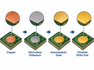
Copper → Electroless Palladium → Autocatalytic Gold

The key difference from ENIG is the absence of electroless nickel. Palladium is deposited over the exposed copper, followed by an autocatalytic gold layer.

This gives EPAG several useful characteristics:

  • nickel-free surface construction;
  • relatively low metallic buildup around fine features;
  • a solderable noble-metal surface;
  • compatibility with qualified wire-bonding processes;
  • potential advantages in RF and flex designs where nickel is undesirable.

The gold process is also important. Autocatalytic gold can continue depositing after the surface has been covered, which gives more control over functional gold thickness than a conventional immersion-gold process.

For this reason, EPAG should be specified as a complete surface-finish system rather than simply as “palladium gold.”

EPAG PCB plating process from copper to electroless palladium and autocatalytic gold

How Is EPAG Plated on a PCB?

The exact chemistry varies between plating systems, but a typical EPAG plating process follows four main stages.

  1. Copper preparation: Exposed copper is cleaned and conditioned. Oxides and contaminants must be removed before palladium deposition.
  2. Electroless palladium plating: Palladium is chemically deposited on the copper without using external electrical current.
  3. Autocatalytic gold deposition: Gold is chemically reduced onto the palladium surface. Unlike a self-limiting immersion reaction, the process can continue building the gold layer.
  4. Cleaning and inspection: The board is rinsed and checked for deposit consistency, thickness, solderability, and application-specific requirements.

The process is more specialized than standard ENIG. A PCB manufacturer needs suitable electroless palladium and autocatalytic-gold chemistry, stable bath control, and reliable thickness measurement.

If EPAG is essential to the design, confirm process availability before finalizing the fabrication drawing.

How Does Autocatalytic Gold Differ from Immersion Gold?

The main difference is how the gold layer grows.

Immersion gold relies on a displacement reaction. Gold deposits while a small amount of the underlying metal is displaced. As the surface becomes covered, deposition slows.

Autocatalytic gold uses a chemical reducing agent, so the gold surface can continue supporting further deposition. This makes it easier to build a thicker functional gold layer where required.

Feature Immersion Gold Autocatalytic Gold
Deposition method Displacement reaction Chemical reduction
Deposit growth Relatively self-limiting Can continue building
Typical role Protection and solderability Functional gold surface
Thickness flexibility More limited Greater
Wire-bond use Process-dependent More suitable when properly qualified

For ordinary solder pads, a thin protective gold layer may be sufficient. Wire-bond pads can require tighter control over gold thickness, purity, and surface condition. That is where autocatalytic gold becomes more valuable.

What Are the Advantages of EPAG PCB Finish?

EPAG is most useful when the design benefits from both a nickel-free stack and a controlled gold surface.
  • Nickel-free construction: useful when nickel is undesirable for electrical, magnetic, or mechanical reasons.
  • Fine-feature compatibility: removing the nickel layer reduces total metal buildup around small pads and tight clearances.
  • Wire-bond capability: properly qualified EPAG processes can support gold, silver, or copper wire bonding.
  • Solderability: palladium and gold provide a solderable, oxidation-resistant surface.
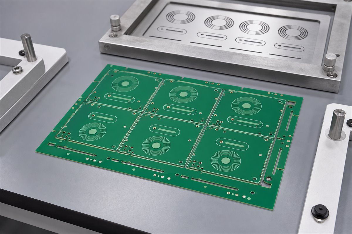
  • RF suitability: removing nickel can be useful on exposed high-frequency conductor areas.
  • Flex compatibility: eliminating the relatively hard nickel layer can help in flex designs where finished areas are close to bending zones.

These advantages matter only when they solve an actual design requirement. For a normal SMT control board, they may not justify a more specialized finish.

What Are the Limitations of EPAG Plating?

The first limitation is availability. EPAG is not offered by every PCB manufacturer that provides ENIG or ENEPIG.

Cost can also be higher because the process uses palladium and gold, and some applications require a more substantial gold deposit.

Specification quality is another concern. For critical applications, “EPAG finish” alone may not be enough. A complete requirement may need to define:

  • palladium thickness;
  • gold thickness;
  • solder-only or wire-bond surfaces;
  • bonding wire material;
  • selective plating areas;
  • storage requirements;
  • acceptance or qualification criteria.

For a standard SMT board with no RF, bonding, fine-feature, or nickel-related constraint, ENIG may remain the more practical choice.
EPAG vs EPIG: What Is the Difference?

EPAG and EPIG are both nickel-free palladium/gold finishes. The main difference is the gold deposition process.

For more detail on the alternative process, see our EPIG PCB surface finish guide.

Feature EPAG EPIG
Full name Electroless Palladium Autocatalytic Gold Electroless Palladium Immersion Gold
Layer concept Cu → Pd → autocatalytic Au Cu → Pd → immersion Au
Nickel layer No No
Gold process Autocatalytic Immersion
Gold build capability Greater More limited
Soldering Suitable Suitable
Wire bonding Strong option with qualified process Possible with suitable process
Fine-feature use Suitable Suitable
Main selection reason Functional gold layer Nickel-free finish with thinner gold

EPIG is often sufficient when the main goal is to remove nickel while maintaining a solderable palladium/gold surface. EPAG becomes more attractive when the gold layer itself needs to perform a more demanding function, especially in wire bonding.
EPAG vs ENIG: Which PCB Surface Finish Should You Choose?

For conventional SMT assembly, ENIG is usually the simpler starting point. EPAG becomes relevant when the nickel layer in ENIG creates a specific design concern.

Our ENIG PCB surface finish guide covers the nickel/gold process and its selection limits.

Selection Factor EPAG ENIG
Layer structure Cu/Pd/Au Cu/Ni/Au
Nickel-free Yes No
Standard SMT Suitable Very common
Wire bonding Suitable with qualified process Not usually the first choice
Fine features Lower metal buildup Nickel increases total deposit thickness
Flex applications Useful where nickel should be avoided Application-dependent
RF applications Attractive when nickel loss matters Common, but contains nickel
Availability Specialized Widely available
Sourcing simplicity Lower Higher

Choose ENIG when you mainly need a flat, solderable, widely supported finish.

Consider an EPAG PCB finish when the project involves:

  • exposed high-frequency conductors;
  • wire bonding;
  • very fine pad geometry;
  • repeated flexing near finished areas;
  • nickel-sensitive design conditions.

Changing from ENIG to EPAG without one of these reasons usually adds complexity without adding much value.

EPAG versus ENIG PCB surface finish comparison

EPAG vs ENEPIG: What Are the Key Differences?

ENEPIG and EPAG can both support soldering and wire bonding, but their metallic structures are different.

Feature EPAG ENEPIG
Layer structure Cu/Pd/autocatalytic Au Cu/Ni/Pd/immersion Au
Nickel No Yes
Palladium Yes Yes
Wire bonding Suitable Widely used
Soldering Suitable Suitable
RF consideration No nickel layer Nickel remains
Flex consideration Attractive where nickel should be avoided Nickel layer remains
Main selection reason Nickel-free functional gold Versatile soldering and bonding

ENEPIG is already a strong option when one PCB needs both soldering and wire bonding. EPAG should not replace it automatically. The case for EPAG becomes stronger when removing nickel provides a measurable electrical, dimensional, or mechanical benefit.

Is EPAG Suitable for Soldering and Wire Bonding?

Yes. EPAG can support both, provided the finish is specified and qualified for the intended assembly process.

For deposit-control context, compare the qualification points in our wire bonding EPIG thickness guide.

For soldering, the gold protects the palladium surface before assembly. The finished pad must still meet the solderability requirements of the selected assembly process.

Wire bonding needs tighter control. Important variables include:

  • gold thickness and purity;
  • surface cleanliness;
  • palladium condition;
  • bonding wire material;
  • wire diameter;
  • ball or wedge bonding method;
  • bonding force and temperature;
  • storage time before assembly.

A surface that looks visually acceptable is not automatically suitable for bonding. For a new production program, prototype bond testing is advisable when the plating chemistry, pad design, bonding wire, or bonding process has changed.

EPAG PCB finish for wire bonding and soldering

Why Is EPAG Used for High-Frequency and RF PCBs?

The main RF reason is simple: EPAG removes the nickel layer.

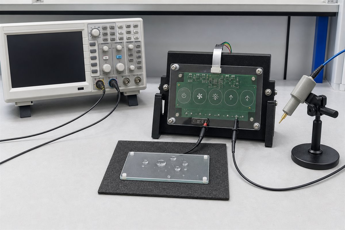
At high frequencies, current becomes concentrated near conductor surfaces because of skin effect. The metallic finish on those surfaces can therefore contribute to conductor loss.

Nickel has much lower conductivity than copper and also has magnetic properties. Removing it from exposed RF conductors can be useful when insertion-loss requirements are tight.

EPAG is worth considering when:

  • RF traces or launches contain exposed finished copper;
  • operating frequency is high;
  • insertion loss is tightly controlled;
  • fine RF features make plating buildup important;
  • nickel-containing surfaces are undesirable.

However, EPAG is not an automatic RF upgrade.

If most transmission lines remain under solder mask and only small component pads receive surface finish, other factors may have a much greater impact, including:

  • copper roughness;
  • dielectric loss;
  • impedance geometry;
  • stackup tolerance;
  • connector launches;
  • via transitions.

The finish should be selected according to where it actually appears in the RF signal path.

EPAG nickel-free finish for RF and high-frequency PCB applications

Can EPAG Be Used on Flex, HDI, and Ceramic PCBs?

Yes, but the reason for using EPAG changes with the PCB technology.

Flex PCB

A nickel-free finish can be useful near bending areas because nickel is relatively hard. EPAG may therefore be considered when finished conductors are exposed to repeated flexing.

HDI and fine-line PCB

Removing the nickel layer can reduce total plated buildup around small pads and closely spaced features. This can help preserve finished geometry in dense layouts.

Ceramic PCB

EPAG can also be considered for ceramic substrates, but compatibility depends on the conductor system rather than the ceramic material alone.

Examples include:

  • direct-bonded copper ceramic;
  • thick-film metallization;
  • thin-film metallization;
  • plated ceramic substrates.

These constructions may require different preparation and plating routes. Do not specify EPAG for a ceramic board based only on the substrate name. Confirm the exposed conductor metallurgy first.

What Should You Specify When Ordering an EPAG PCB?

An EPAG RFQ needs more information than a note saying “gold finish.”

Provide the PCB manufacturer with:

  • Surface finish: EPAG / Electroless Palladium Autocatalytic Gold
  • Board type: rigid, flex, rigid-flex, HDI, ceramic, etc.
  • Base material and stackup
  • Board thickness
  • Copper weight
  • Minimum trace and spacing
  • Minimum pad dimensions
  • Required palladium thickness, if controlled
  • Required gold thickness
  • Soldering requirements
  • Wire-bond requirements and wire material
  • Selective plating areas, if any
  • Controlled impedance or RF requirements
  • Inspection or qualification standard
  • Prototype and production quantities

Avoid copying a plating thickness from an older drawing unless you know why it was specified. Excessive gold can increase cost, while insufficient control can create problems in bonding applications.

At EBest Circuit, we can review the fabrication data, stackup, finish requirement, assembly method, and qualification needs during quotation. We confirm whether the proposed finish route fits the intended soldering, bonding, RF, or flex application before production.

EPAG PCB RFQ checklist with stackup, gold thickness, wire bond, RF requirement and quantity

FAQs About EPAG PCB Finish

Is EPAG a nickel-free PCB surface finish?

Yes. EPAG uses electroless palladium over copper followed by autocatalytic gold, without an electroless nickel layer.

What is the difference between EPAG and EPIG?

Both are nickel-free palladium/gold finishes. EPIG uses immersion gold, while EPAG uses autocatalytic gold, which provides greater flexibility for building a functional gold layer.

Can EPAG be used for gold wire bonding?

Yes, provided the plating process, gold thickness, surface condition, and bonding parameters are qualified for the application.

Is EPAG better than ENIG for high-frequency PCBs?

Not always. EPAG can be useful when nickel on exposed RF conductors contributes to loss. If most RF traces are covered by solder mask, material loss, copper roughness, geometry, and connector transitions may matter more.

How should EPAG be specified on a PCB drawing?

Write Electroless Palladium Autocatalytic Gold (EPAG) and add controlled palladium or gold thickness where required. Wire-bond areas, bonding material, selective plating, and qualification requirements should also be identified.

How Can EBest Circuit Review Your EPAG PCB Requirements?

EPAG is valuable when its nickel-free structure and autocatalytic gold layer solve a real bonding, geometry, flex, or RF requirement. For routine SMT boards, a more widely available finish may remain the better purchasing choice.

Send us your Gerber or ODB++ files, stackup, quantity, finish specification, wire material, RF conditions, and deposit or qualification requirements. We will review manufacturability, confirm process availability, and prepare a quotation without assuming that one finish fits every design.

You may also like