PCB manufacturing PCB manufacturing
Home > Blog

PCB Panel Design

PCB Panel Sizes Explained: How to Maximize Board Yield and Reduce Manufacturing Cost
Wednesday, June 17th, 2026

There is no universal PCB panel size. Common fabrication references include 18 × 24 in, but the best delivery panel is the size that fits the usable fabrication area, every SMT machine, and the chosen depaneling process. In this article, “panel yield” means boards obtained from the available panel area—not first-pass manufacturing yield.

Efficient PCB panel sizes use material well without becoming difficult to print, place, reflow, inspect, or separate. The practical target is not the largest possible array; it is the layout with the lowest stable cost per acceptable board. Calculations must use the real usable area, and the fabricator and assembler should approve the same controlled drawing.

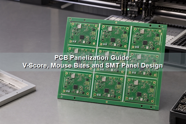
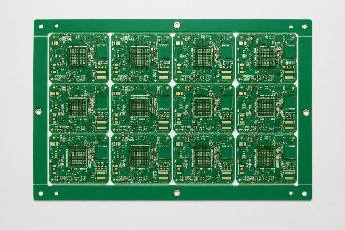
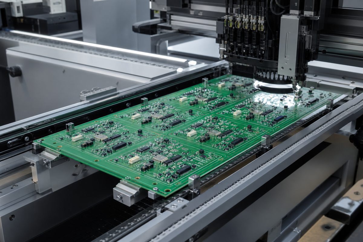
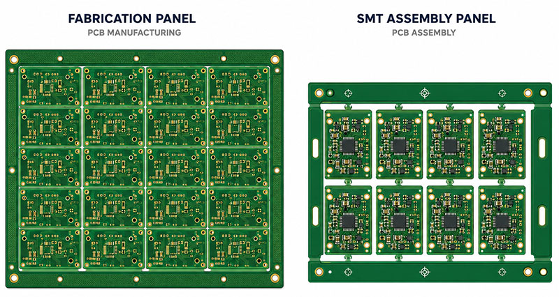
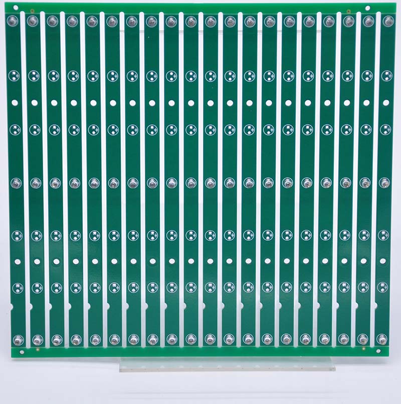
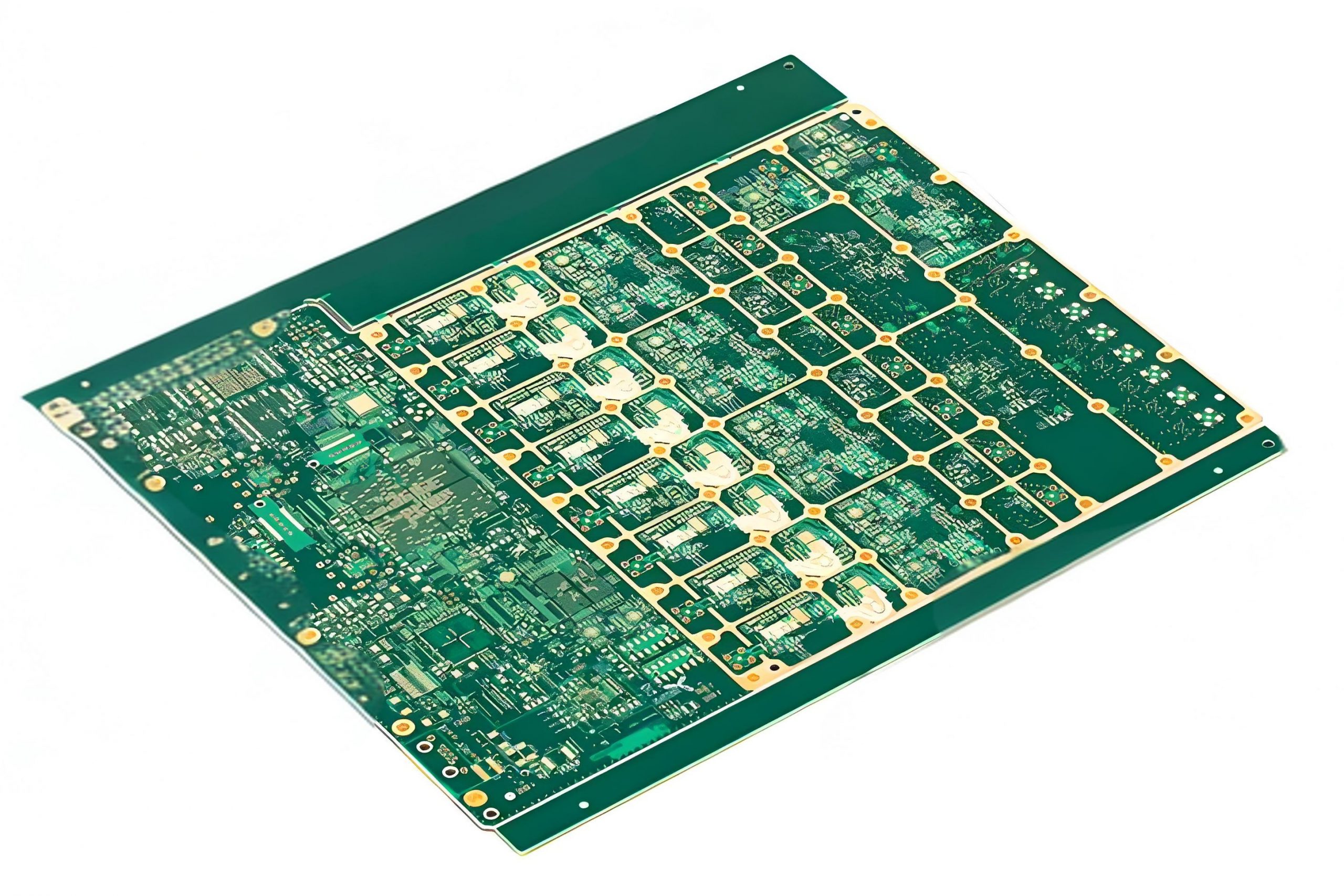
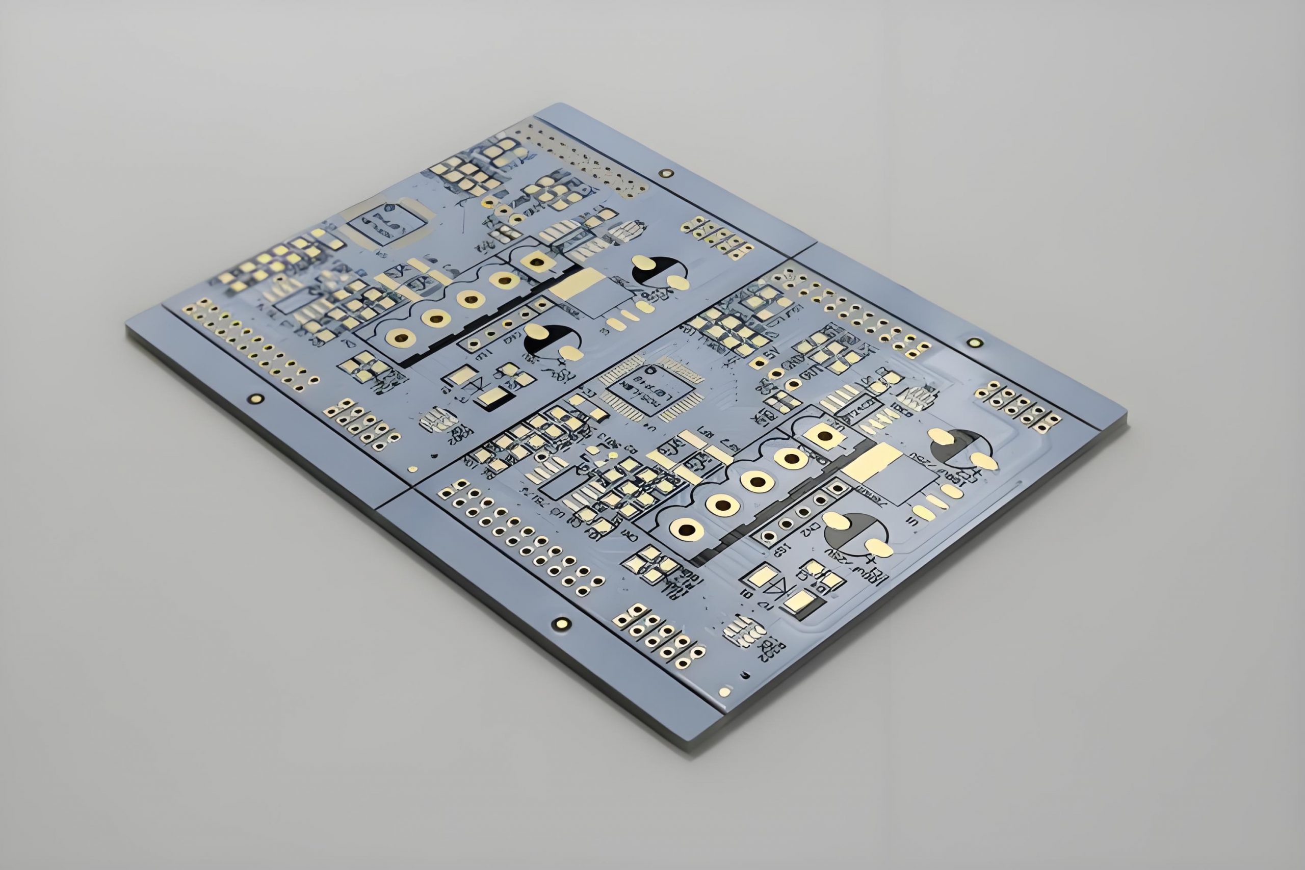
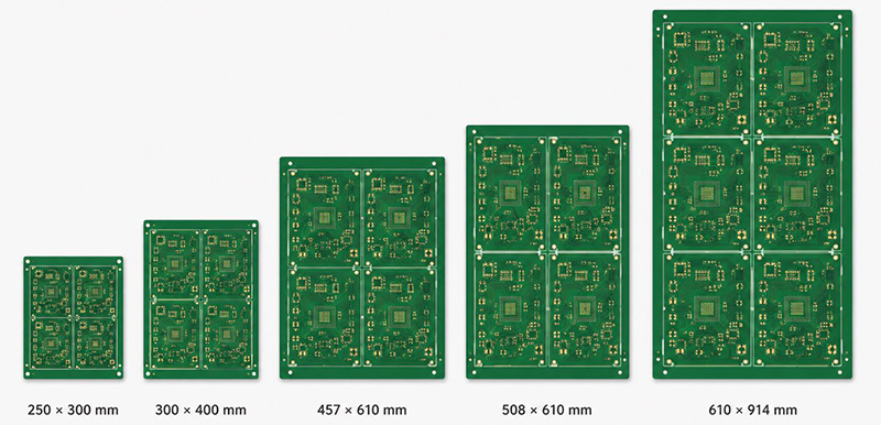
PCB panel sizes shown on a production-ready circuit board array

What Are the Common PCB Panel Sizes, and Is There a Universal Standard?

Common PCB panel sizes are reference formats, not a universal standard. Fabricators select working panels around laminate and equipment constraints. Assemblers usually receive a smaller customer array designed for their line.

Category Reference format How to use it What to confirm
Fabrication format 24 × 18 in (610 × 457 mm) Manufacturing-panel reference Confirm the usable nesting area
Fabrication format 12 × 18 in (305 × 457 mm) Manufacturing-panel reference Confirm process margins and coupons
Fabrication format 24 × 9 in (610 × 229 mm) Manufacturing-panel reference Confirm material and process availability
Fabrication format 12 × 9 in (305 × 229 mm) Manufacturing-panel reference Confirm whether it is a working or delivery panel

These dimensions are planning references rather than universal standards. Use them to estimate how individual boards may nest within fabrication material, not as automatic SMT delivery-panel dimensions. When comparing quotations, ask each supplier to identify the full working panel, usable production area, boards per delivery panel, and final shipped dimensions separately.

What Is the Difference Between Fabrication and Assembly Panel Sizes?

A fabrication panel is a manufacturing workpiece; an assembly panel is the array that travels through SMT production. One fabrication panel may contain several customer arrays, while the assembly line handles each delivery panel separately.

Term Purpose Main constraint Buyer check
Full fabrication panel Starting or working material Fabrication equipment and laminate format Confirm whether dimensions are raw or process-ready
Usable fabrication area Area available for boards and process features Margins, coupons, tooling, and routing Request confirmed usable width and height
Delivery panel Array shipped to the customer or assembler Rails, board count, separation, and packing Approve the final dimensioned drawing
SMT assembly panel Carrier through printing, placement, reflow, and inspection The narrowest equipment window in the line Confirm minimum, maximum, thickness, and support limits

A fabricator’s maximum dimension is not automatically the preferred SMT panel size. A manufacturable board may still require rails, a carrier, or a smaller array.

How Much Usable Area Does a PCB Panel Provide?

Usable area equals the full panel dimensions minus all reserved process zones. The simplest planning formulas are:

Usable width = full width − left margin − right margin
Usable height = full height − top margin − bottom margin

An 18 × 24 in sheet with 0.5 in reserved on every side would provide a simplified 17 × 23 in rectangle. Production margins may also include coupons, plating features, tooling holes, fiducials, router access, identification, and test structures. The fabricator must confirm the real nesting boundary.

PCB panel usable area with board array, edge rails, and tooling holes

How Do Rails, Spacing, Tooling Holes, and Fiducials Affect Panel Dimensions?

Every handling and process feature consumes space, but removing it can make the array unbuildable. Add these elements before calculating the number of boards per panel.

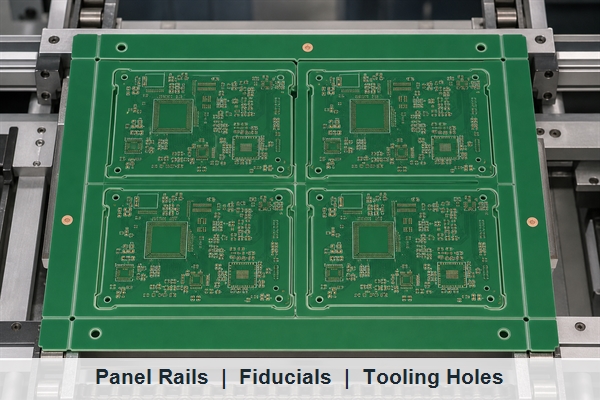
  • Edge rails: provide conveyor support, clamping space, global fiducials, and clearance from edge-mounted components.
  • Board spacing: provides room for V-scoring, router paths, tabs, and the selected final-edge condition.
  • Tooling holes: locate the panel in assembly, test, or depaneling fixtures; their size and position are line-specific.
  • Global fiducials: align the complete panel for solder-paste printing and component placement.
  • Local fiducials: support board-level or fine-pitch alignment when the assembly process requires them.

The released drawing should show overall dimensions, array count, rails, gaps, separation paths, tabs, tooling holes, fiducials, orientation, coupons, labels, and bad-board marking. Use only assembler-approved rail and tooling values.

How Do You Calculate Boards per Panel, Yield, and Material Utilization?

Calculate both board orientations using usable dimensions and the actual process gap. Let usable panel dimensions be Uw × Uh, board dimensions be Bw × Bh, and the required board gap be G:

Columns = floor((Uw + G) ÷ (Bw + G))
Rows = floor((Uh + G) ÷ (Bh + G))
Boards per panel = columns × rows

Orientation can change the number of boards that fit without changing the panel size. For example, consider a 300 × 400 mm delivery panel with 10 mm rails on every side, a 70 × 95 mm board, and a 2 mm routing gap. The simplified usable area is 280 × 380 mm. Calculating both orientations gives the following result:

  • 0° orientation: floor(282 ÷ 72) gives 3 columns, while floor(382 ÷ 97) gives 3 rows, producing 9 boards.
  • 90° orientation: floor(282 ÷ 97) gives 2 columns, while floor(382 ÷ 72) gives 5 rows, producing 10 boards.
  • Full-panel utilization: (10 × 70 × 95) ÷ (300 × 400) equals 55.4% for the 2 × 5 layout.

The 90° layout fits one additional board and raises the calculated material utilization. However, board count alone is not enough to approve it. Rail direction, conveyor support, copper balance, component orientation, panel stiffness, and depaneling stress must still be checked. If the 2 × 5 array is too flexible or difficult to separate consistently, the lower-count 3 × 3 layout may deliver the more stable production result.

How Do V-Scoring and Tab Routing Affect PCB Panel Size?

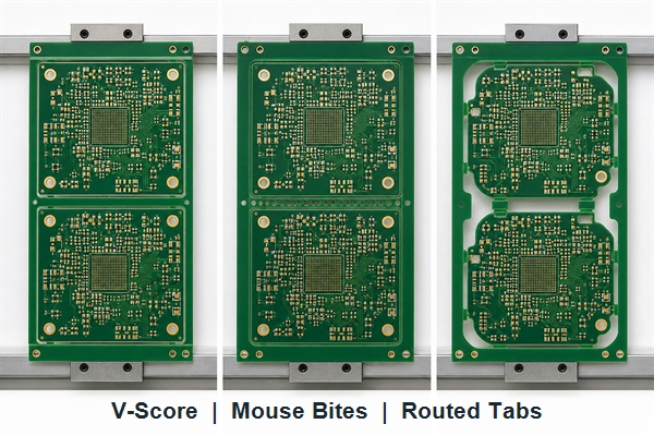
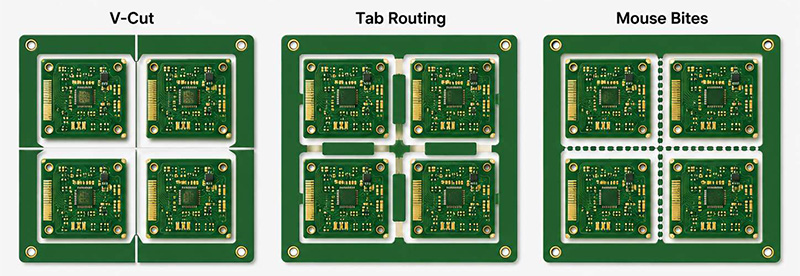
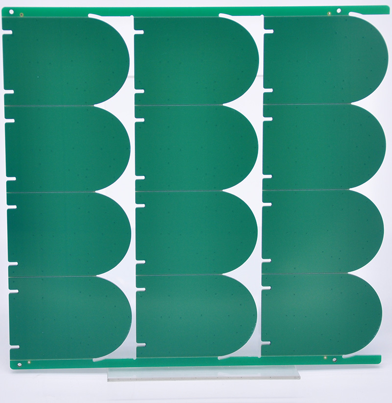
V-scoring can support close straight-line arrays, while tab routing needs router clearance and controlled connection points. The correct method depends on outline geometry, edge quality, component clearance, panel stiffness, and separation stress.

Decision factor V-scoring Tab routing
Best-fit geometry Rectangular arrays with continuous straight separation lines Curved, irregular, or selectively separated outlines
Hybrid use Can be combined with local routing when straight scoring alone cannot release the outline Can complement V-scoring around irregular features
Board spacing Often allows zero profile-to-profile spacing, subject to supplier rules Requires a router path plus controlled tabs or mouse bites
Panel stability Depends on board thickness, remaining web, rail design, and score-line arrangement Routing removes material, so tab number, position, and frame width must maintain rigidity
Edge result Leaves a scored separation edge May leave tab or mouse-bite witness marks that need allowance or finishing
Component clearance Bending during separation can stress components and solder joints near the score Router access, tab cutting, and protruding edge components require clearance
Release controls Specify score angle, remaining thickness, tolerance, and depaneling direction Specify cutter diameter, tab width and position, mouse-bite pattern, and permitted edge residue
Approval evidence Dimensioned panel drawing plus fabricator and assembler confirmation Dimensioned panel drawing plus routing, support, and depaneling confirmation

Do not select the method only by the number of boards it fits. Review the final edge requirement, component distance from break lines, permitted separation force, and whether the remaining frame is rigid enough for assembly.

How Do Board Thickness and Copper Balance Affect Panel Stability?

Panel stability depends on the complete array—not board thickness alone. A thin board may run reliably in a compact, well-supported panel, while a thicker panel can still twist if routing removes too much material or heavy components are concentrated on one side. The critical combination is panel span, thickness, routed area, rail width, tab placement, component mass, and support through printing, placement, reflow, inspection, and separation.

Copper balance matters because copper and laminate respond differently during heating and cooling. A large copper area on one side or one region can create uneven thermal expansion and contraction, increasing bow or twist. The objective is not to force identical copper everywhere; it is to avoid severe asymmetry while preserving electrical performance. Stack-up symmetry, copper distribution, and any balancing patterns added in process areas should be reviewed by the fabricator rather than changed only for appearance.

  • Check the unsupported span: Long, narrow arrays and large routed openings are more likely to sag between conveyor rails or tooling supports.
  • Map component weight: Transformers, inductors, connectors, heat sinks, and other heavy parts can bend a weak frame during acceleration, reflow, or handling.
  • Protect process accuracy: Excess movement can affect stencil contact, paste release, placement height, AOI focus, probe alignment, and depaneling position.
  • Strengthen the correct feature: A smaller array, wider rails, better tab locations, temporary crossbars, pallet support, or a carrier may be more effective than simply increasing board thickness.
  • Validate under production conditions: Review the populated panel, not only the bare array, and confirm that it remains supported at the hottest and mechanically weakest process step.

For a new design, ask the fabricator and assembler to review the same panel drawing before fixtures are released. If the panel is long, thin, heavily routed, or component-heavy, a trial build should confirm flatness, paste printing, conveyor transport, reflow support, and separation quality before the array is frozen for volume production.

How Does PCB Panel Size Affect Manufacturing Cost?

A larger array lowers cost only when the additional boards pass through fabrication, assembly, testing, and separation without adding disproportionate risk or tooling expense. Material utilization is important, but it is only one part of the unit-cost calculation.

  • Fabrication material: Better nesting can reduce laminate waste, but oversized panels may require a less efficient working-panel layout or a special material format.
  • Routing and scoring: V-scoring is efficient for continuous straight lines; routed outlines add machine time, cutter travel, tabs, and possible edge finishing.
  • Assembly throughput: More boards per cycle can reduce loading, printing, placement, and inspection overhead per board, provided the panel remains within the stable operating window.
  • Tooling and support: A larger or weaker panel may require a stencil change, carrier, pallet, support pins, test fixture, or dedicated depaneling tool.
  • Failure exposure: One printing, reflow, handling, or test incident affects every board on the panel. Increasing the array count raises the value exposed in a single event.
  • Labor after assembly: Manual separation, filing mouse-bite remnants, sorting, retesting, and packaging can erase a small material-saving advantage.

Compare alternatives with panel-related cost per acceptable board = total panel fabrication, assembly handling, tooling allocation, test, separation, and expected loss ÷ acceptable boards delivered. Use the same order quantity and delivery condition for every option.

For example, an illustrative 12-board array costing $240 through separation equals $20 per acceptable board if all 12 pass. A 15-board array costing $285 also equals $19 per board when all pass, but rises above $20 if one board is routinely lost or extra rework is required. The numbers are not market prices; they show why quotation comparison must include acceptable output rather than board count alone. For broader quotation planning, review the main custom PCB cost factors.

How Do You Choose the Most Cost-Effective PCB Panel Size?

The most cost-effective PCB panel size is the option with the lowest repeatable cost per acceptable board. Use the following decision sequence:

  • Lock the board definition: Confirm the outline, thickness, stack-up, copper weight, surface finish, edge connectors, overhanging components, and areas that cannot receive tabs or score lines.
  • Separate the panel definitions: Record the fabrication working panel, usable nesting area, and final delivery panel independently so quotations are compared on the same basis.
  • Define the process envelope: Confirm supported length, width, thickness, weight, conveyor direction, clamping area, stencil print area, fixtures, and depaneling equipment.
  • Choose the separation method: Match V-scoring, tab routing, mouse bites, or a hybrid layout to the outline, edge-quality requirement, component clearance, and permitted separation stress.
  • Build the complete panel geometry: Add rails, gaps, fiducials, tooling holes, coupons, labels, bad-board marks, and test access before calculating board count.
  • Compare realistic orientations: Calculate 0° and 90° layouts and any approved mixed orientation, then reject arrangements that interrupt continuous score lines or weaken the frame.
  • Check populated-panel stability: Review copper balance, routed openings, heavy components, unsupported span, carriers, and support at printing, reflow, inspection, testing, and separation.
  • Compare total unit cost: Include material, processing, tooling allocation, assembly handling, testing, depaneling labor, edge finishing, packaging, and expected loss—not only boards per panel.
  • Release one controlled drawing: Freeze dimensions, orientation, rails, tooling, separation features, markings, and delivery condition only after fabrication and assembly approval.

This workflow turns common PCB panel sizes into project-specific options. It also prevents a fabrication-efficient array from being redesigned after it reaches the provider of custom PCB assembly services.

What Should You Submit for a PCB Panel Review?

A useful panel review needs the board data, assembly constraints, quantity, and required delivery condition. Send:

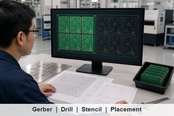
  • Production data: Gerber, ODB++, IPC-2581, or another complete reviewable PCB package.
  • Board definition: outline, dimensions, thickness, stack-up, copper weight, and critical edge features.
  • Assembly requirements: populated side, overhanging components, conveyor direction, and known line limits.
  • Panel preferences: required board count, permitted optimization, rails, fiducials, tooling, and marking.
  • Separation requirements: V-score or routing preference, final-edge quality, and depaneling responsibility.
  • Commercial scope: prototype and production quantities, test method, fixture constraints, and delivery format.

If the delivery array is not fixed, submitting single-board production data allows the fabricator to propose a panel for joint DFM approval. This is safer than locking dimensions before the assembly equipment and separation method are known.

Frequently Asked Questions About PCB Panel Sizes

Q1: Should the designer create the panel, or should the manufacturer do it?

A1: Let the manufacturing partners propose or verify the production panel unless you control the complete process. You may submit a preferred array, but fabrication utilization, assembly handling, fixtures, and separation still require approval.

Q2: Can several different PCB designs be combined in one delivery panel?

A2: Yes, when the supplier accepts a mixed-design array. The boards normally need compatible materials, stack-up, thickness, finish, process flow, traceability, assembly sequence, and test strategy. Pricing rules may still count them as separate designs.

Q3: What does an X-out board mean in an assembled panel?

A3: An X-out identifies a known nonconforming circuit within an otherwise usable panel. Decide before quotation whether X-outs are allowed, how they are marked, whether placement skips them, and how many are acceptable per panel.

Q4: Can mouse-bite remnants interfere with an enclosure?

A4: Yes, residual tabs can exceed the desired finished edge or create a rough contact point. Define the permitted edge residue and whether trimming, routing, sanding, or inspection is required before shipment.

Q5: How close can components or copper be to a break line?

A5: Use the fabricator’s clearance rule and add space for the actual separation tool and board flex. Edge connectors, ceramic capacitors, heavy parts, antennas, and overhanging components often require additional protection.

Q6: Can a castellated-edge module be panelized?

A6: Usually, but the castellated edges must remain accessible and undamaged. A hybrid layout using routed openings, controlled tabs, and straight score lines may be needed. Approve plating, support, and separation details before release.

Q7: Is panelization worthwhile for a manually assembled prototype?

A7: Only when the panel improves handling, repeatability, or test efficiency enough to justify separation work. A few simple boards assembled by hand may be easier to order individually.

Q8: Can rotated boards be mixed within the same panel?

A8: Sometimes, if the arrangement remains manufacturable and assembly-compatible. Check score-line continuity, component orientation, conveyor direction, copper balance, labeling, programming, and test-fixture access.

Q9: Should rails be removed before the PCBAs are delivered?

A9: The delivery condition should follow your downstream operation. Keep rails when they are still needed for testing, programming, coating, transport, or final assembly; otherwise specify individual-board delivery and edge-finish expectations.

Q10: Which changes require a new panel revision?

A10: Reapprove the panel when board outline, thickness, quantity strategy, assembler, equipment path, component overhang, tooling, test method, separation process, or delivery condition changes. Keep the drawing revision synchronized with the production data.

Conclusion

PCB panel sizes should be selected from verified usable area, assembly-line limits, separation requirements, and mechanical stability. Calculate both orientations, but do not approve the highest board count until rails, support, copper balance, tooling, and total production cost are reviewed. One drawing jointly approved by fabrication and assembly provides the clearest path to predictable output.

If you are sourcing reliable PCB or PCBA manufacturing, send your Gerber/ODB++, BOM, quantity, stack-up, assembly details, programming method, and test requirements to sales@bestpcbs.com for engineering review and a quotation.

You may also like

Optimized PCBA Panel Strategies for Reliable Mass Production
Tuesday, February 17th, 2026

A PCBA panel, or printed circuit board assembly panel, is a larger board that holds multiple identical or different PCB units for streamlined manufacturing. This article will explore optimized panel strategies to maximize reliability, yield, and cost-effectiveness in high-volume production, covering design guidelines, common mistakes, and efficiency calculations.

What are the most common pain points in PCB panelization?

  • Assembly errors: Misalignment and solder defects caused by poor panel design.
  • Low utilization: Board material wasted due to inefficient panel layouts.
  • Process inefficiency: Excessive manual handling slows down production.
  • Stress and breakage: Improper depaneling leads to bent boards or cracked parts.
  • Cost overruns: Yield loss and rework inflate the real panel cost.

Addressing these challenges requires a systematic approach.​ Here are five key solutions from a seasoned PCBA manufacturer’s perspective:

  • DFM-driven panel design: Apply clear panelization guidelines early with your manufacturer.
  • Utilization optimization: Maximize panel fill before fabrication.
  • Automation-ready panels: Design for SMT, testing, and depaneling automation.
  • Controlled breakaway methods: Use appropriate V-scoring or tab routing with stress relief.
  • Total cost evaluation: Optimize for yield and throughput, not panel price alone.

As a professional PCBA manufacturer with 20 years of experience in high-mix, high-volume production, EBest Circuit (Best Technology) partners with clients from the design stage to implement optimized PCBA panel​ strategies. Our engineering team leverages advanced software and proven PCB panel design​ principles to ensure maximum reliability and efficiency for your mass production runs. For a consultation on your next PCB assembly project, pls feel free to contact us at sales@bestpcbs.com.

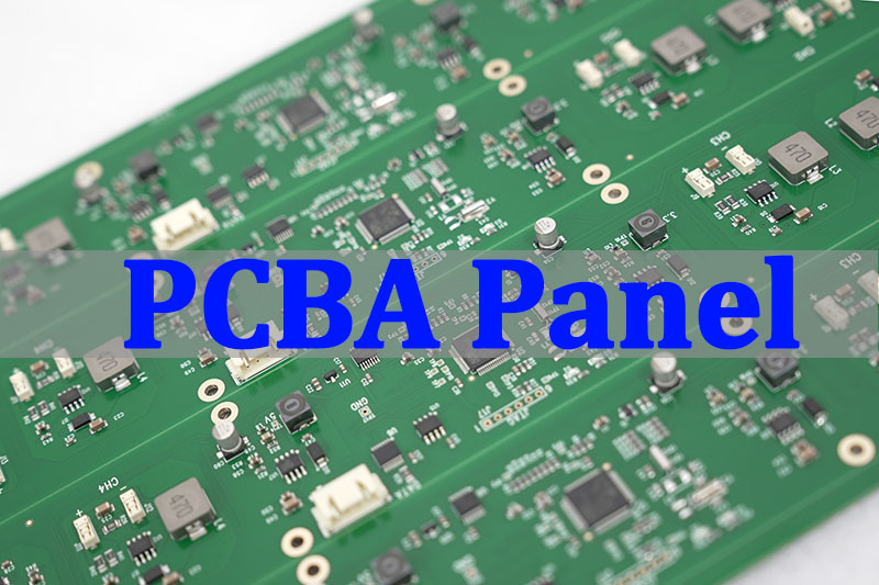
PCBA Panel

What Is a PCBA Panel and Why It Matters in Mass Production?

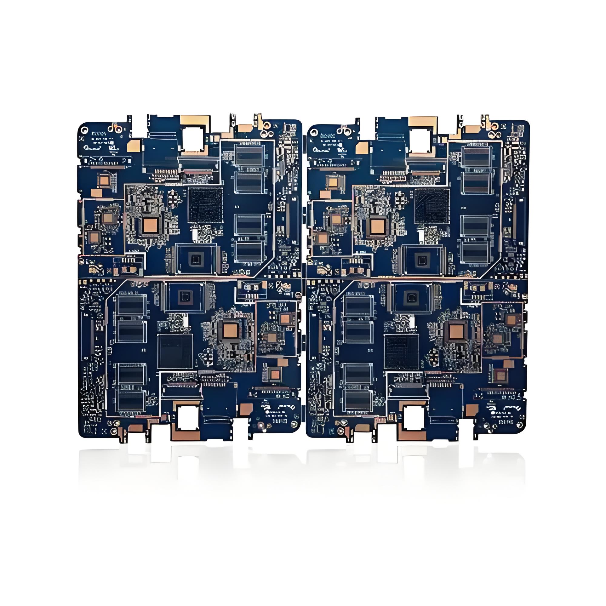
A PCBA panel is a carrier board that combines multiple individual PCBs into a single unit for efficient assembly and testing.

  • Single-unit processing: Multiple PCBs are assembled together through SMT, wave soldering, and testing.
  • Higher throughput: Panelization allows many boards to be populated and soldered simultaneously.
  • Mechanical stability: Small or irregular boards remain stable during automated handling.
  • Reduced handling risk: Fewer manual steps lower the chance of damage and human error.
  • Process standardization: Consistent panel formats improve repeatability and quality control.
  • Cost and scale enablement: Optimized panels support mass production with predictable cost and output.
PCBA Panel

What PCB Panelization Methods Are Used in Modern PCBA Lines?

PCB panelization​ is the technique of arranging multiple board designs onto a single panel. The choice of method directly impacts assembly ease, depaneling quality, and board integrity. Modern lines primarily use three methods, often in combination.

  • Tab Routing (Mouse Bites):​ Individual boards are connected by small, perforated tabs. This method is ideal for complex board shapes or when components are placed very close to the edge.
  • V-Scoring (V-Grooving):​ A V-shaped groove is cut partially through the panel material, leaving a thin web of material to hold boards together. It allows for very fast, clean depaneling with specialized equipment.
  • Mixed Panelization:​ Combines V-scoring for straight edges and tab routing for complex contours within the same PCB panel array.

The table below summarizes the key differences:

MethodBest ForDepanelingEdge Quality
Tab RoutingIrregular shapes, edge componentsBreak by hand or machine; slowerRequires smoothing (nubs remain)
V-ScoringRectangular/regular shapes, high speedFast snap or machine separationVery clean, straight edges
MixedComplex panels with mixed requirementsCombination of methodsVaries by edge type

Choosing the right method depends on your board’s geometry, component placement, and available depaneling equipment at the factory.

How Are PCB Panel Sizes Determined for Different Board Designs?

Determining the optimal PCB panel sizes​ is a balancing act between machine compatibility, material utilization, and assembly efficiency. It’s not a one-size-fits-all calculation. Key factors include:

  • Equipment Constraints:​ The panel must fit within the minimum and maximum dimensions of SMT pick-and-place machines, reflow ovens, wave solder carriers, and testing fixtures. Standard panel sizes often align with common equipment specs (e.g., 330mm x 250mm).
  • Material Utilization:​ The primary goal is to fit as many units as possible with minimal waste. This is where a PCB panel utilization calculator​ becomes invaluable.
    Utilization (%) = (Total area of individual boards / Total panel area) x 100.
    Aim for >80% utilization where possible.
  • Board Shape and Array:​ The shape of your single PCB dictates how it can be nested or arrayed on the panel. Rectangular boards tile efficiently, while odd shapes may require a PCB panel array​ with rotation or different orientations to fill space.
  • Process Requirements:​ Space must be allocated for tooling holes (for machine alignment), fiducial marks, test coupons, and breakaway tabs or V-score channels.
  • Handling and Depaneling:​ Very large panels may be difficult to handle or may warp in reflow; very small or thin panels may lack rigidity. The size must allow for safe, reliable depaneling.

In practice, manufacturers like Best Technology use software to simulate different layouts and calculate PCB panel​ configurations that deliver the best compromise of all these factors for your specific design.

What Is a PCB Panel Array and How Does It Improve Assembly Efficiency?

A PCB panel array​ refers to the specific arrangement or matrix of individual PCB copies on the panel. It is the heart of assembly optimization. A well-planned array improves efficiency in several concrete ways:

  • Maximized Throughput:​ By populating 10, 20, or even 50 boards in one machine cycle, the effective placement rate of components is multiplied.
  • Reduced Setup Time:​ Programming and calibrating machines for one panel is vastly faster than for hundreds of individual boards.
  • Consistent Quality:​ All boards on a panel experience identical process conditions (solder paste application, reflow profile, wave solder exposure), minimizing unit-to-unit variation.
  • Streamlined Testing:​ Automated test systems (like flying probe or fixture-based testers) can sequence through all boards on a panel with minimal movement, speeding up validation.
  • Optimized Material Flow:​ Handling, storing, and moving panels is logistically simpler than managing loose boards, reducing risk of damage and mix-ups.

For example, a 2×5 array processes ten boards at once, effectively making the assembly line ten times faster for the placement and soldering stages compared to single-board processing. This multiplicative effect is why panel array design is critical for cost-effective mass production.

How Do PCB Panelization Guidelines Affect Yield and Cost Control?

Adhering to robust PCB panelization guidelines​ is a direct lever for controlling yield and cost. These guidelines standardize the process to prevent defects and waste.

Key Panel Design Guidelines:

  • Clearance & Spacing:​ Maintain sufficient spacing between board edges (typically 3mm minimum) and from components to panel borders/scores (2mm minimum) to prevent interference during assembly and depaneling.
  • Tooling & Fiducials:​ Include standardized, unplated tooling holes and global/fine-pitch fiducial marks for precise machine alignment across the entire panel.
  • Depaneling Considerations:​ Design breakaway tabs with proper size (e.g., 5mm x 5mm) and spacing. For V-scoring, ensure components are kept away from the score line.
  • Panel Strength:​ Ensure the panel frame is rigid enough to prevent warping or sagging during high-temperature reflow soldering. This may require strategic tab placement or a thicker panel core.
  • Waste Strips:​ Include waste strips on at least two opposing sides to provide edge grip for conveyor systems and space for process coupons.

Ignoring these guidelines can lead to misprinted solder paste, misaligned components, cracked solder joints during depaneling, and panel warpage—all of which directly scrap boards and increase cost per functional unit. A disciplined approach to panelization is a non-negotiable aspect of reliable mass production.

What Factors Influence PCB Panel Price in Production Runs?

While the unit PCB panel price​ is part of the total cost, it’s influenced by several interconnected factors that savvy buyers should understand:

  • Panel Size and Material:​ Larger panels use more base material (FR-4, Rogers, etc.), directly increasing cost. The choice of material itself is a major cost driver.
  • Number of Layers:​ A multilayer PCB panel board​ is more expensive to fabricate than a double-sided one due to increased lamination and drilling steps.
  • Panel Utilization:​ Low utilization means you are paying for wasted material. A higher utilization percentage achieved through smart PCB panel design​ lowers the effective cost per individual board.
  • Special Processes:​ Additional requirements like controlled impedance, gold plating, blind/buried vias, or heavy copper increase the fabrication complexity and cost of the panel.
  • Order Quantity:​ Economies of scale apply. The cost per panel decreases with higher volume runs, as setup and tooling costs are amortized over more units.

Understanding this breakdown helps in making informed trade-offs. For instance, a slightly larger panel with higher utilization might yield a lower cost per final assembled board than a smaller, inefficient panel.

What Common PCB Panelization Mistakes Lead to Assembly or Yield Issues?

Even experienced teams can stumble on panelization. Here are common pitfalls and how to avoid them:

  • Ignoring Machine Capabilities:​ Designing a panel larger than the printer or pick-and-place machine can handle leads to immediate production stoppage.
  • Insufficient Clearance:​ Placing components or traces too close to routing paths or V-score lines guarantees damage during depaneling.
  • Weak Panel Frame:​ A flimsy frame can cause the panel to warp in reflow oven, leading to poor soldering and making automated depaneling impossible.
  • Missing Fiducials:​ Without proper fiducials, especially for fine-pitch components, placement accuracy suffers, causing shorts or open circuits.
  • Poor Tab Design:​ Too few or weak tabs can cause boards to detach during processing; too many or poorly positioned tabs make depaneling difficult and stressful for the boards.
  • Overlooking Test Access:​ Failing to provide space or clearance for in-circuit test (ICT) probes or fixtures on the panel can make electrical testing cumbersome or impossible.

The remedy is always early collaboration and a formal DFM check with your PCBA manufacturer before panel design is finalized.

How Should PCB Panel Design Be Optimized for PCBA Assembly?

Optimizing PCB panel design​ requires a holistic view of the entire assembly and test process. Follow these principles:

  • Optimize for SMT Assembly:​ Ensure the panel is rigid, flat, and has reliable fiducials. Orient all boards in the same direction on the panel to minimize pick-and-place head rotation and maximize speed.
  • Facilitate Soldering:​ Consider thermal mass distribution. A panel with a very dense area next to a sparse area may solder unevenly. Balance the layout if possible.
  • Integrate Testing Strategy:​ Design the panel to accommodate your test method. Include test points accessible in the panelized form or design it for easy break-in before testing if needed.
  • Plan for Depaneling:​ Choose the breakaway method (V-score vs. tabs) early in the layout process and design the board outlines accordingly. Provide clear, clean break lines.
  • Maximize Real-Estate:​ Use every available millimeter wisely. Nest different board designs together (if volume allows) or adjust the board outline slightly to improve utilization without affecting functionality.
  • Standardize Where Possible:​ Using consistent panel sizes and tooling hole patterns across multiple projects can reduce factory setup time and cost for your products.

By addressing these areas, you create a panel that is not just a carrier, but an active tool for manufacturing excellence.

PCBA Panel

To conclude, a PCBA panel​ is the strategic backbone of efficient electronics manufacturing, enabling the simultaneous processing of multiple boards to achieve scale, consistency, and cost control. This article has outlined the core strategies—from selecting the right PCB panelization​ method and optimizing PCB panel sizes​ with a PCB panel calculator, to avoiding costly design mistakes—that are essential for reliable mass production.

With in-house PCB and PCBA manufacturing, EBest Circuit (Best Technology) has 20 years of proven experience serving Medical, Industrial Control, Robotics, and IoT PCBA projects. Backed by 1,000+ supply-chain partners, we deliver assured quality and on-time production. Pls feel free to reach out to our engineering and sales team anytime at sales@bestpcbs.com​ for a detailed consultation.

FAQs about PCBA Panel

What Is the Purpose of a PCBA Panel in Assembly?

A PCBA panel groups multiple individual PCBs into a single carrier to improve assembly efficiency, handling stability, and consistency during SMT, soldering, and testing.

When Should a Project Use a Custom PCBA Panel Instead of Single Boards?

A custom PCBA panel is recommended for small boards, irregular shapes, or mass production, where automation, throughput, and cost control are critical.

What Is the Difference Between a PCBA Panel and a Single PCB?

A PCBA panel contains multiple individual PCBs processed together, while a single PCB is assembled and handled one board at a time, resulting in lower efficiency and higher handling risk.

Does PCBA Panelization Affect Testing and Inspection?

Yes. A well-designed PCBA panel allows inline testing, AOI, and functional testing to be performed more efficiently before depaneling, improving overall test consistency.

Who Should Define the PCBA Panel Design—The Designer or the Manufacturer?

PCBA panel design is best finalized collaboratively. Designers define functional requirements, while manufacturers optimize panel layout for assembly, depaneling, and yield.

You may also like

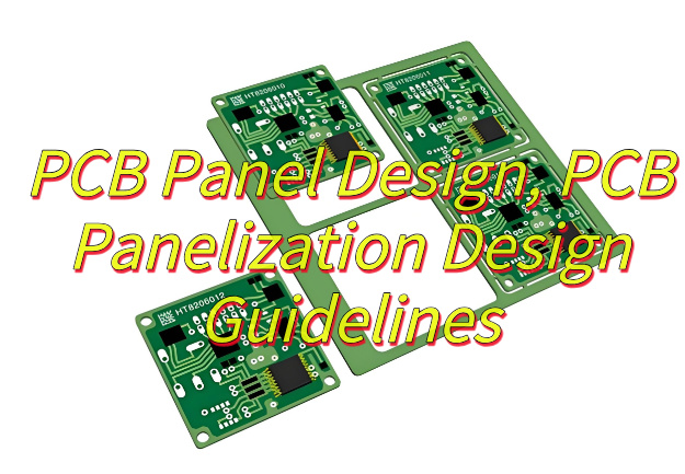
PCB Panel Design, PCB Panelization Design Guidelines
Friday, June 13th, 2025

Did you know PCB panel design can reduce manufacturing costs by up to 30% while improving production efficiency? This guide covers essential panelization techniques, software tools, and Gerber integration strategies for optimized PCB manufacturing.

At EBest Circuit (Best Technology), we understand the critical challenges PCB manufacturers face – material waste driving up costs, inefficient panel layouts slowing production, and delayed deliveries impacting project timelines. Our expert PCB panel design services directly address these pain points by maximizing panel utilization (HDI, flex-rigid) through advanced nesting algorithms, typically achieving 15-30% material savings that translate to immediate cost reductions. With specialized engineers who have processed over 5,000 panel designs, we implement manufacturing-optimized configurations (tab routing, V-scoring, mixed-technology panels) that maintain quality while accelerating production cycles. Our rapid 72-hour standard turnaround for panelization designs, combined with automated DRC validation, ensures clients avoid costly respins and meet tight deadlines. We go beyond basic panelization by integrating test coupons, serialization, and depaneling solutions that streamline the entire production workflow. By transforming panel design from an afterthought into a strategic advantage, we help clients achieve faster time-to-market, lower per-unit costs, and reliable high-volume production – all supported by our dedicated technical team throughout the product lifecycle. Welcome to contact us now: sales@bestpcbs.com.
What Is PCB Panel Design?

PCB panel design is the strategic process of arranging multiple printed circuit boards onto a single manufacturing panel to optimize production efficiency while ensuring structural integrity and assembly compatibility. This essential practice in PCB panelization design guidelines involves carefully spacing individual boards with breakaway tabs, routing channels, or perforated connections that allow clean separation after component assembly, while incorporating tooling holes, fiducials, and clearance margins to facilitate automated handling during fabrication. The effectiveness of PCB panel design directly impacts material utilization, manufacturing yield, and depaneling reliability, requiring balanced consideration of board spacing, panel thickness, and breakaway method selection to prevent stress fractures or component damage. Proper PCB panel design follows industry-proven layouts that account for thermal expansion during soldering, mechanical stress during depaneling, and alignment precision for high-density interconnects, making it a foundational element in mass production workflows where even minor miscalculations in panelization can cascade into significant quality issues. Following established PCB panelization design guidelines ensures that the transition from design files to mass-produced boards maintains dimensional accuracy and functional reliability across the entire manufacturing cycle.

PCB Panel Design

Why Do PCB Panel Design?

Here are the practical benefits of PCB panel design explained with clear business advantages:

  • Cost Efficiency in Manufacturing‌: PCB panel design allows multiple boards to be produced simultaneously on a single panel, reducing material waste and optimizing production time. This directly lowers per-unit manufacturing costs while maintaining quality standards.
  • Improved Assembly Reliability‌: Following PCB panelization design guidelines ensures stable board handling during automated assembly. The panel structure prevents warping and misalignment during soldering, reducing costly defects.
  • Enhanced Testing Efficiency‌: PCB panel design enables batch testing of multiple boards at once, cutting quality control time by up to 50% compared to individual board testing. This accelerates time-to-market while maintaining defect detection accuracy.
  • Material Utilization Optimization‌: Strategic board arrangement within panels minimizes substrate waste. Proper PCB panelization design guidelines help utilize up to 95% of raw material, significantly reducing procurement expenses.
  • Logistics and Handling Savings‌: Standardized panel sizes simplify packaging and transportation, decreasing shipping damage risks and storage requirements. This creates measurable savings in supply chain operations.
  • Thermal Process Stability‌: PCB panel design ensures even heat distribution during reflow soldering, preventing localized overheating that could compromise solder joints. This improves long-term product reliability.
PCB Panel Design

What Are the Different Types of PCB Panels?

Here are the primary types of PCB panels used in manufacturing, each offering distinct advantages for cost and production efficiency:

Single-Unit Panel‌

  • Contains identical PCBs arranged uniformly
  • Maximizes material usage when producing high volumes of the same design
  • Simplifies assembly line processes through standardized handling

Mixed Panel (Multi-Circuit Panel)‌

  • Combines different PCB designs on one panel
  • Ideal for low-volume production of varied products
  • Reduces setup costs by processing multiple designs simultaneously

Breakaway Tab Panel (Tab-Routed Panel)‌

  • Uses small perforated tabs to connect individual boards
  • Allows manual separation without specialized equipment
  • Cost-effective for prototypes and small batches

V-Scored Panel‌

  • Features V-shaped grooves between boards for clean separation
  • Enables high-speed depaneling with minimal stress on components
  • Reduces material waste compared to routing

Plated Half-Cut Panel‌

  • Incorporates partially cut copper connections between boards
  • Provides electrical continuity during testing while allowing easy breakage
  • Lowers testing costs through panel-level verification

Flexible Panel (Rigid-Flex Panel)‌

  • Combines rigid and flexible sections in one panel
  • Eliminates connectors between board segments
  • Reduces assembly time and improves reliability in complex designs

How to Design A PCB Panel?

Designing an efficient PCB panel requires balancing functionality, manufacturability, and cost efficiency. Below is a structured, step-by-step approach to creating a panel layout that reduces expenses, accelerates production, and ensures reliability.

1. Optimize Panel Layout and Material Usage

  • Maximize Board Density: Arrange PCBs within standard panel sizes (e.g., 18×24 inches) using design software to minimize unused space. Combine small and large boards or rotate irregular shapes to fill gaps.
  • Benefit: Reduces material waste by up to 35%, lowering per-unit costs.
  • Standardize Orientation: Align all boards in the same direction to simplify automated assembly processes, reducing machine setup time.

2. Incorporate Robust Tooling Rails

  • Design Sturdy Rails: Add 5–10mm-wide rails along panel edges to provide structural stability during handling and manufacturing.
  • Benefit: Prevents panel warpage, ensuring consistent drilling and soldering quality.
  • Add Fiducial Markers: Place 1mm-diameter copper fiducials on rails to guide automated optical inspection (AOI) and component placement machines.

3. Engineer Breakaway Tabs and Separation Features

  • Strategic Tab Placement: Use 2–3mm tabs to connect individual PCBs. Avoid placing tabs near delicate components or high-density trace areas.
  • Benefit: Enables easy depanelization without damaging boards, reducing labor costs.
  • Include V-Scoring or Perforations: Add V-shaped grooves or perforated lines between boards for clean, stress-free separation.

4. Address Thermal and Mechanical Stress

  • Stress Relief Design: Integrate slots or cutouts near heavy components (e.g., connectors) to prevent panel distortion during reflow soldering.
  • Benefit: Reduces soldering defects and rework expenses.
  • Thermal Management: Distribute thermal vias around heat-sensitive components to improve heat dissipation and maintain temperature uniformity.

5. Streamline Testing and Traceability

  • Universal Test Points: Align test pads (e.g., 1mm gold-plated copper) across all boards for efficient in-circuit testing (ICT).
  • Benefit: Accelerates quality control, reducing test time by up to 40%.
  • Identification Markers: Include QR codes, batch numbers, or part numbers on rails for easy traceability during assembly and shipping.

6. Validate with Design for Manufacturability (DFM) Tools

  • Run Simulations: Use DFM software to detect issues like insufficient spacing, improper tab placement, or non-compliant drill sizes.
  • Benefit: Prevents costly redesigns and ensures first-pass success.
  • Prototype Testing: Produce a small batch to validate assembly processes and identify bottlenecks before full-scale production.

7. Finalize Comprehensive Documentation

  • Detailed Panel Drawings: Include dimensions, tab locations, and scoring specifications in manufacturing files.
  • Benefit: Ensures consistency across batches and reduces supplier miscommunication.
  • Supplier Guidelines: Provide clear instructions on depanelization methods (e.g., manual vs. automated) to avoid misinterpretation.

What Are the Commonly Used PCB Panelization Design Software?

Selecting the right software can significantly streamline the PCB panelization process, ensuring efficiency, accuracy, and cost-effectiveness. Below is a curated list of widely used tools, each offering unique features to address different design needs:

Altium Designer

  • Core Strengths: Seamlessly integrates panelization tools with its PCB design ecosystem. Features include automated panel layout wizards, real-time 3D visualization, and built-in design rule checks (DRC) to prevent errors.

  • Why It Stands Out: Ideal for complex, high-density boards. Its rule-driven engine ensures consistent spacing and alignment across panels, reducing rework.

Cadence Allegro

  • Core Strengths: Specializes in advanced panelization for high-speed and RF designs. Offers dynamic array optimization and embedded thermal/mechanical stress analysis.
  • Why It Stands Out: Critical for applications requiring signal integrity, such as 5G or automotive electronics. Its simulation tools predict panel behavior under thermal cycling.

Mentor Graphics PADS

  • Core Strengths: Combines auto-routing with panel-specific features like tab design and scoring line generation. Includes DFM validation to catch issues early.
  • Why It Stands Out: User-friendly for mid-sized teams. Its cost-effective licensing makes it popular for consumer electronics and IoT devices.

Zuken CR-8000

  • Core Strengths: Excels in multi-board panelization with 3D MCAD co-design. Supports thermal simulation and mechanical stress analysis for large panels.
  • Why It Stands Out: Perfect for aerospace or industrial projects where electrical and mechanical teams collaborate closely.

KiCad (Open Source)

  • Core Strengths: Free, open-source tool with basic panelization support. Includes edge cuts, tooling holes, and fiducial markers via its Pcbnew editor.
  • Why It Stands Out: A budget-friendly option for startups or hobbyists. Active community forums provide tutorials and troubleshooting.

AutoCAD Electrical

  • Core Strengths: Flexible for custom panel shapes. Exports DXF/DWG files for seamless integration with manufacturing equipment.
  • Why It Stands Out: Useful for non-standard layouts or legacy systems requiring CAD compatibility.

Valor NPI (Siemens)

  • Core Strengths: Advanced DFM software focusing on manufacturability. Analyzes solder paste stencils, test points, and cost drivers.
  • Why It Stands Out: Reduces prototyping cycles by 50% through predictive analytics, saving time and money.

What Is the Basic Rule of PCB Panelization Design?

Creating an effective PCB panel requires adherence to foundational rules that ensure manufacturability, cost efficiency, and reliability. Below are the essential guidelines to optimize your panelization design:

  1. Uniform Board Orientation
  • Rule: Align all PCBs consistently in one direction.
  • Why: Simplifies automated assembly (e.g., pick-and-place machines), reduces setup time, and minimizes placement errors.
  • Impact: Lowers labor costs and accelerates production throughput.
  1. Maximize Panel Utilization
  • Rule: Arrange boards to minimize empty space within standard panel sizes (e.g., 18×24 inches).
  • Why: Reduces material waste and cuts raw material costs by up to 30%.
  • Impact: Directly lowers per-unit production expenses and supports sustainability.
  1. Robust Tooling Rails
  • Rule: Include 5–10mm-wide rails along panel edges.
  • Why: Provides structural stability during drilling, soldering, and handling.
  • Impact: Prevents panel warpage and ensures precise component alignment.
  1. Strategic Breakaway Tabs
  • Rule: Connect boards with 2–3mm tabs, avoiding sensitive component areas.
  • Why: Enables easy, damage-free separation post-production.
  • Impact: Reduces labor costs and scrap rates during depanelization.
  1. V-Scoring or Perforations
  • Rule: Add V-shaped grooves or perforated lines between boards.
  • Why: Facilitates clean, stress-free separation without mechanical damage.
  • Impact: Ensures boards detach smoothly, maintaining edge quality.
  1. Thermal and Mechanical Stress Relief
  • Rule: Integrate stress-relief features (e.g., slots) near heavy components (e.g., connectors).
  • Why: Prevents panel distortion during high-temperature processes like reflow soldering.
  • Impact: Reduces soldering defects and rework, improving first-pass yield.
  1. Design for Manufacturability (DFM) Validation
  • Rule: Use DFM tools to check for issues like insufficient spacing or non-compliant drill sizes.
  • Why: Identifies and resolves design flaws early, preventing costly redesigns.
  • Impact: Reduces prototyping iterations and ensures smooth, error-free production.
PCB Panelization Design

How to Evaluate the Rationality of PCB Panelization Design?

Below are methods about how to evaluate the rationality of PCB panelization design:

  1. Material Utilization Rate
  • Metric: Calculate the ratio of usable PCB area to total panel area.
  • Evaluation: Aim for ≥85% utilization. Lower rates indicate inefficient layout design.
  • Impact: Directly reduces material waste and lowers production costs.
  1. Manufacturing Throughput
  • Metric: Measure the time required for assembly, soldering, and testing per panel.
  • Evaluation: Streamlined designs minimize machine downtime and enable parallel processing.
  • Impact: Accelerates production, reducing labor costs and time-to-market.
  1. Depanelization Ease
  • Metric: Assess the simplicity of breaking tabs or scoring lines.
  • Evaluation: Designs with clean V-scoring or perforations reduce labor and damage risks.
  • Impact: Simplifies post-production processes and minimizes scrap.
  1. Structural Stability
  • Metric: Verify the inclusion of tooling rails (5–10mm width) and fiducial markers.
  • Evaluation: Rails prevent warpage; fiducials ensure precise alignment with automated systems.
  • Impact: Improves yield and reduces rework during assembly.
  1. Thermal and Mechanical Compliance
  • Metric: Analyze stress-relief features near heavy components (e.g., slots, thermal vias).
  • Evaluation: Ensure designs withstand reflow soldering without distortion.
  • Impact: Reduces soldering defects and enhances reliability.
  1. Testability and Traceability
  • Metric: Check for standardized test points (e.g., 1mm gold-plated pads) and QR codes.
  • Evaluation: Test points must align across all boards for efficient in-circuit testing (ICT).
  • Impact: Streamlines quality control and simplifies defect tracking.
  1. Cost-Benefit Ratio
  • Metric: Compare total production costs (material, labor, rework) against savings from panelization.
  • Evaluation: Aim for a 15–30% cost reduction per unit compared to single-board production.
  • Impact: Ensures a positive return on investment (ROI) for panelization efforts.
PCB Panelization Design?

Should I Design Panels in My PCB Gerber?

No, you should not design panels directly within your PCB Gerber files. Gerber files are intended to define the individual board’s layout—traces, pads, and layers—while panelization is a manufacturing optimization step best handled separately. Including panelization details like tooling holes, scoring lines, or board arrays in Gerbers risks confusing fabricators, as they expect single-board definitions. Instead, provide a dedicated panelization drawing alongside your Gerber files to specify requirements such as board quantity per panel, spacing, tab placement, and fiducial locations. This approach allows manufacturers to adapt the panel layout to their equipment (e.g., panel size limits, drilling capabilities) while ensuring your design intent is respected. Embedding panelization in Gerbers may also lead to errors, such as accidental inclusion of panel-specific features in the final PCBs. By separating panelization guidelines from core design data, you maintain clarity in the Gerber files and empower manufacturers to optimize production for cost efficiency and quality. Always confirm with your fabricator that they accept panelization instructions as a standalone document to streamline collaboration and avoid misinterpretation.

You may also like