Electrical circuit diagram symbols represent components and their electrical connections, not the physical shape of a finished board. To read them, identify each symbol, follow its connected nets, then check values, polarity and pin numbers. For a PCB project, those details must remain consistent from the schematic through the component list, footprint and assembly drawing.

What Are Electrical Symbols in Circuit Diagrams?
Electrical symbols are graphical shorthand for functions such as resistance, energy storage, switching and amplification. A circuit diagram uses electrical symbols to represent components and lines to show the intended connections between their terminals. A resistor drawing identifies a resistor; its label and linked part record specify which resistor belongs on the board.
Electrical symbols and electronic symbols overlap. A battery, switch or connector can appear in both a machine control schematic and a small electronic assembly. The difference is the system being described, not a completely separate alphabet. This guide concentrates on electronic circuit symbols used in PCB-related drawings rather than building floor-plan notation.
Common Circuit Symbols and Functions
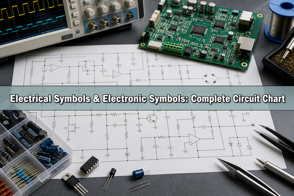
The most useful starting point is a circuit symbols chart that pairs the drawing with its function and the detail you must verify. The illustration shows basic electrical circuit diagram symbols; the table explains how to interpret them without treating the shape as a complete component specification. Together they form an electrical symbols chart with reading checks, not a list of interchangeable parts.
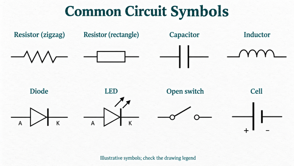
| Component | Typical drawing cue | Function and reading check |
|---|---|---|
| Resistor | Zigzag or rectangle | Limits current or establishes voltage ratios. Read resistance, tolerance and power rating. |
| Capacitor | Two plates; polarized versions may show + | Stores charge and supports filtering or coupling. Check capacitance, voltage rating and polarity. |
| Inductor | Coil; some versions include core markings | Stores magnetic energy. Check inductance, current rating and the specified part. |
| Diode / LED | Diode with cathode bar; LED adds outward arrows | Diode conduction is directional. LED arrows represent emitted light, not extra terminals. |
| Cell / battery | Unequal parallel lines; repeated pairs for a battery | Provides DC energy. The longer line indicates the positive side; voltage requires a label. |
| Switch | Contact points and movable contact | Makes, breaks or changes a connection. Identify the pole, throw and shown state. |
| Fuse | Small inline fuse element, convention-dependent | Overcurrent protection. Read current, voltage and time-current characteristics. |
| Transistor / IC | Device-specific symbol or pin-labelled block | Switches, amplifies or processes signals. Confirm pin names, numbers and supply connections. |
These schematic symbols of electronic components describe electrical roles. Ratings and package dimensions belong in the component data and bill of materials (BOM); they cannot be inferred from how large the symbol is drawn.
What Is the Symbol for Electric Wire?
A straight line represents an electrical connection. A filled junction dot normally joins intersecting wires; crossing lines without a dot normally remain separate in modern electronic schematics. Older drawings may use a curved crossover or different junction conventions, so check the legend before tracing an unfamiliar design.
Wires that share a net label can be connected even when no continuous line runs across the page. In hierarchical designs, local, global and sheet-level labels have different scopes. Matching visible text alone does not prove that two labels on different sheets form one net.
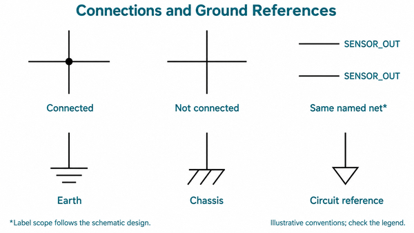
A bus groups named signals; it is not a copper short between every signal inside it. A no-connect marker on an unused pin also differs from a junction dot. When checking an electrical schematic drawing, use net highlighting or the connection list to resolve an ambiguous intersection instead of guessing from a low-resolution image.
How Do Power, Battery and Ground Symbols Differ?
Power symbols identify sources or supply nets, while a ground symbol identifies a reference or grounding connection. Neither the position of a symbol nor the word GND alone establishes a physical connection to protective earth.
What is the symbol for battery?
The battery circuit symbol commonly uses alternating long and short parallel lines. One pair represents a cell; multiple pairs represent a battery. The number of drawn pairs is not a reliable cell-count specification, and the symbol does not establish voltage or chemistry. Read the stated supply value and battery part information.
What are symbols for AC and DC current?
A sine-wave mark commonly indicates AC, while a solid line above a dashed line indicates DC in equipment notation. Circuit source symbols may instead show a sine wave, +/− signs or a directional arrow inside a circle. The letter I is the usual current symbol in equations; it is not a component or a substitute for an AC/DC rating.
Earth, chassis and circuit-reference symbols serve different purposes. Circuit reference is the node used for voltage measurements; chassis refers to the frame or enclosure; protective earth is part of a safety connection. They may be connected by a deliberate design, but must not be assumed interchangeable. Separate AGND and DGND labels likewise require an intentional connection strategy, not an automatic split in the PCB ground plane.
How Do You Read Resistor, Capacitor and Inductor Symbols?
Read the symbol first, then the component value and its surrounding connections. Passive components with identical drawings can perform very different jobs depending on where they sit in the circuit.
Resistor symbols and adjustment arrows
The resistor schematic symbol can be a zigzag or rectangle. A diagonal adjustment arrow indicates a variable element; a potentiometer normally has two end terminals and a third wiper terminal. A fixed resistor connected from a digital input to a supply is a pull-up, while the same component in series with an LED limits current.
For readers asking what schematic symbol represents a current limiter, there is no single answer for every circuit. A series resistor can limit current, but regulated current limiting may use an IC, transistor and sense resistor. The circuit function must be established from the connections and ratings.
Capacitor and magnetic-component details
A non-polarized capacitor symbol uses two plates. Polarized versions may add a + sign and sometimes a curved plate; the explicit polarity marking and component datasheet take priority. A ceramic capacitor is not made polarized simply by the orientation of its label.
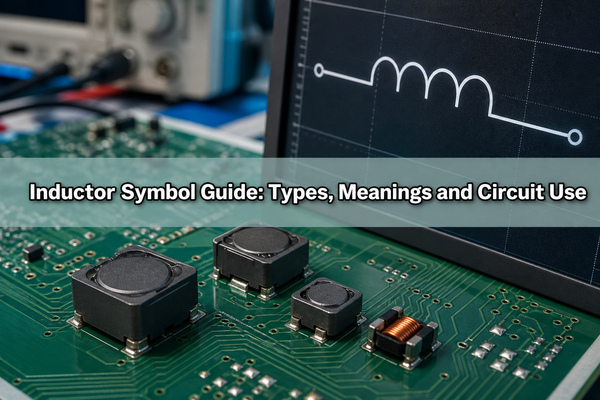
An inductor symbol is commonly a coil. Added core markings distinguish some symbol variants; two coupled windings indicate a transformer. Dots on coupled windings describe relative winding polarity, not junctions connecting the windings. A symbol alone does not specify saturation current, insulation rating or the complete magnetic construction.
How Do Diode and LED Symbols Show Polarity?
The diode’s bar identifies the cathode, commonly labelled K; the other terminal is the anode, A. Conventional forward current passes from anode to cathode when the device is appropriately forward biased. Rotating the symbol changes its position on the page, not the terminal identities.
The LED symbol adds arrows pointing away from the diode to indicate emitted light. A photodiode uses arrows pointing toward it. Zener and Schottky devices use modified cathode markings, so a generic diode sketch is not enough to identify the correct BOM part.
Before PCB assembly, match the schematic polarity to the footprint pad numbering and the component drawing. Do not assume every library assigns pin 1 to the same terminal. Our rectifier diode guide covers the additional voltage, current and recovery checks needed for rectification circuits.
How Do Switch, Relay and Protection Symbols Work?
A switch symbol shows which contacts connect in the illustrated state. SPST has one switched path; SPDT connects one common terminal to either of two alternatives. Pole and throw describe the contact arrangement, not the number of decorative lines or package pins.
What is the symbol for a single pole switch?
For a simple SPST switch, two contact points and a movable line show an open or closed path. Normally open and normally closed refer to a defined normal condition, commonly an unactuated switch or de-energized relay. Read any drawing note that specifies a different state.
In electrical control circuit diagram symbols, a relay coil and its contacts may be drawn far apart and linked by a common reference. Their physical separation on the schematic does not mean they are separate devices. A limit switch adds an actuation function; the associated mechanical state still needs to be understood.
A fuse and a circuit breaker symbol both concern protection, but they do not describe interchangeable parts. A fuse is normally replaced after operation; a breaker may be reset after the fault is addressed. Contact symbols do not establish safe working voltage, interrupting capacity or regulatory approval.
How Are Transistors, Logic Gates and IC Pins Represented?
Active-device symbols identify functions and terminal relationships. The pin names and part-specific pinout are what connect the drawing to the real package.
On a bipolar transistor, B, C and E identify base, collector and emitter. The emitter arrow points outward for NPN and inward for PNP. A MOSFET uses gate, drain and source, and its symbol may show a body diode. Its appearance is not permission to swap source and drain.
Logic circuit symbols distinguish AND, OR, inversion and other functions. A small output bubble indicates inversion; a triangle without that bubble may be a buffer. An operational amplifier also has a triangular body, but its + and − inputs and supply requirements identify a different function. Those input signs are not the amplifier’s power pins.
Large ICs are often rectangular blocks with named and numbered pins. One physical package may be split into several schematic units, including a separate power unit. For fine-pitch devices on HDI PCBs, accurate pin-to-pad mapping must precede escape routing: the logical symbol does not determine the required via structure.
Why Do IEC and ANSI-Style Schematic Symbols Look Different?
Different symbol conventions can represent the same electrical function. The familiar resistor rectangle is associated with IEC-style drawings, while the zigzag is common in ANSI/IEEE-style drawings. Neither shape alone changes resistance or selects a regional component.
IEC 60617 concerns graphical symbols for electrotechnical diagrams. CAD libraries and legacy documents may use different variants, particularly for logic, grounding and switches. Follow the drawing’s stated convention and legend rather than expecting every electrical schematic symbols chart to look identical.
For an unfamiliar symbol, first check its reference, terminal names and linked part number, then compare it with the library definition. A copied image can omit a polarity mark, inversion bubble or connection dot that changes the interpretation.
What Do R1, C1, Values and Pin Numbers Mean?
A reference designator identifies one component instance; a value describes an electrical property; a pin number maps a terminal to the package. Mixing these three kinds of circuit notation is a common cause of schematic-to-BOM errors.
| Marking | Meaning | What to confirm |
|---|---|---|
| R1, C1, L1, D1 | Common references for resistor, capacitor, inductor and diode | The same reference identifies the same part in the BOM and PCB files. |
| U1, Q1, J1 | Common references for an IC, transistor and connector | Project conventions vary; check the library and assembly drawing. |
| 4k7 / 4R7 | 4.7 kΩ / 4.7 Ω | Do not confuse a multiplier with a reference prefix. |
| 100 nF / 0.1 µF | The same capacitance value | Voltage, dielectric and tolerance still need specification. |
| Pin 1 / A / K | Package number or functional terminal name | Check the selected symbol-to-footprint mapping; do not infer numbering from left/right position. |
| DNP / DNI | Do not populate / do not install | Ensure assembly variants agree across BOM, drawing and placement data. |
A value is not a complete purchasing description. Two 10 kΩ resistors can differ in package, tolerance and power rating. For multi-unit devices, make sure the separate units still resolve to one physical part and that all supply pins are accounted for.
How to Read Circuit Diagrams?
Trace a complete path from the supply through the load and back to the return, checking the state of each component along the way. This gives the individual symbols a circuit-level meaning.
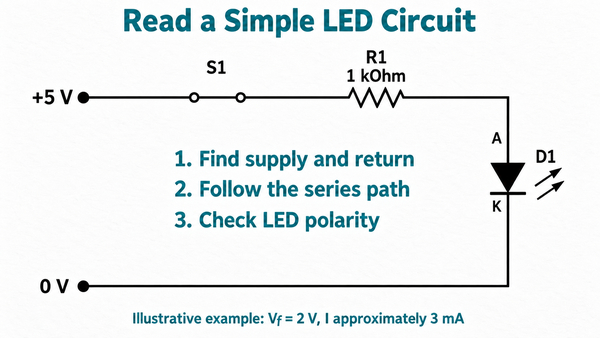
- Find the +5 V supply and 0 V return. The source is connected at the two labelled terminals.
- Follow S1. It is shown closed, so the series path continues through R1.
- Read R1 as 1 kΩ. It limits the current rather than setting the LED voltage directly.
- Identify D1’s anode and cathode. The cathode bar is on the return side.
- Estimate current using the stated assumptions: I = (5 V − 2 V) / 1,000 Ω = 3 mA.
- Check what changes when S1 opens: the series path is broken and the ideal steady-state LED current becomes zero.
The 2 V LED forward drop is an illustrative assumption, not a value for every LED. Actual current depends on the selected LED, supply tolerance, resistor tolerance and temperature. The resistor dissipates approximately 9 mW in this example; its selected rating still needs suitable operating margin.
To draw a circuit diagram, place symbols from the appropriate library, connect their electrical pins, add values and annotate references. Run electrical rules checking (ERC), then inspect the circuit function. ERC can find certain connection conflicts but cannot prove that the design will perform as intended.
How Do Schematic Symbols Become a Manufacturable PCB?
A schematic defines logical connectivity; a PCB layout defines physical pads, tracks, vias and placement. A wiring diagram instead emphasizes connections between terminals, cables or assemblies. Wiring diagram symbols can overlap with schematic notation, but the documents answer different questions.
For FR4 printed circuit boards, the net information must be translated into copper geometry with suitable spacing, current capacity and return paths. A neat electrical schematic diagram does not, by itself, establish board thickness, layer stack-up or trace dimensions.
At EBest Circuit (Best Technology), we provide PCB assembly services for SMT, through-hole and mixed assemblies. Our assembly capability includes 01005 SMD components and BGA pitch down to 0.25 mm, subject to review of the actual package, PCB and process requirements. Clear polarity, pin mapping and assembly-variant information are particularly important for small components and dense packages.
For a fabrication and assembly quotation, send your current Gerber and drill files, BOM with manufacturer part numbers, pick-and-place data and assembly drawing. Include the schematic and any special test or polarity requirements so we can discuss ambiguities against the same design revision. A schematic screenshot alone is not a complete manufacturing package.
Reading electrical circuit diagram symbols is the first step; consistent component and manufacturing data keep that meaning intact on the finished board. Send your project files to sales@bestpcbs.com for PCB and assembly review.
You may also like




Tags: circuit diagram symbols, PCB Assembly, pcb design, Schematic Symbols