Conductive ink for PCB applications is a printable material that contains electrically conductive ingredients, commonly carbon, silver, or copper particles. After its specified drying, curing, or sintering process, it can form a contact surface, an interconnect, or an intentionally resistive pattern.
The right choice depends on what the finished feature must do. A keypad contact needs repeatable switching and wear performance; a printed connection needs an acceptable voltage drop. Ink grade, geometry, printing, cure, and adhesion must be considered together before replacing a copper feature.
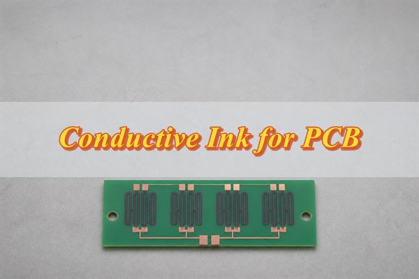
What Is Conductive Ink for PCB?
Conductive ink deposits an electrically functional film where it is printed. In particle-filled formulations, a liquid vehicle carries the conductive material, while a binder helps hold the finished film together and attach it to the substrate. Electrical performance depends on the resulting conductive network and the specified processing conditions.
Ordinary solder mask is insulating, and PCB legend ink provides markings. Conductive ink instead carries current or provides a deliberate resistance. On conventional boards, it commonly supplements copper; in additive printed electronics, printed material may form much of the circuit itself.
Where Is Conductive Ink Used on PCBs?
Common roles include contact surfaces, short printed connections, and resistive features. Each role needs a different acceptance test:
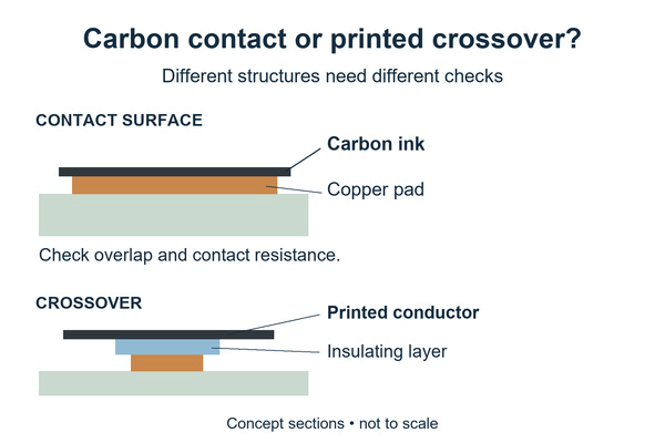
- Keypads and switches: carbon-covered copper contacts can meet a conductive rubber actuator in a remote control or control panel. Membrane switches also use printed conductors on suitable films. Measure the assembled contact under its intended force or travel.
- Low-current jumpers and crossovers: a printed conductor can connect separated pads. Where it crosses another conductor, an insulating layer must separate them. Check both jumper continuity and isolation at the crossing.
- Printed resistors, sensors, and heaters: select a grade for the required resistance and stability. A carbon contact ink is not automatically a precision resistor material.
- Flexible printed electronics: a compatible conductor can form interconnects on flexible substrates. Qualify the ink, substrate, attachment, and protective layers together under the required bending conditions.
Carbon, Silver or Copper: Which Conductive Ink Should You Choose?
Choose by the electrical function first, then compare formulations that suit the same substrate and production process. The comparison below groups inks by their main conductive filler. The descriptions are typical tendencies; finished-film data must decide the selection.
| Ink type | Typical electrical behavior | PCB uses | Main trade-off |
|---|---|---|---|
| Carbon / graphite | Usually more resistive than metal-filled inks | Contacts and resistive patterns | Resistance can limit interconnect use |
| Silver | Often suited to lower-resistance printed paths | Printed interconnects | Material cost; verify attachment process |
| Copper | Can form low-resistance metallic paths | Printed conductors | Oxidation and process control |
Silver–carbon blends provide another way to adjust resistance and contact behavior. They should be selected from measured product data, rather than assigned the properties of either pure filler. Binder chemistry also matters: two silver inks can differ substantially in flexibility, cure schedule, and solvent compatibility.
A common overgeneralization is that every copper ink requires nitrogen processing. Copprint describes copper formulations that sinter in air. That is a product-specific capability, not permission to process other copper inks in the same way. Likewise, “silver” does not by itself guarantee low-temperature curing or solderability.
Can Conductive Ink Replace Copper Traces?
Yes, for selected features that meet the electrical, mechanical, and environmental requirements. It is not a drop-in replacement for an existing copper layout.
Useful candidates: short low-current connections, printed jumpers, and additive interconnects can be considered when their resistance and attachment are acceptable. Carbon also provides contact and resistive functions alongside copper routing.
Keep copper unless the alternative is qualified: high-current supply paths, very low-resistance connections, and high-speed controlled-impedance routing need more than a DC continuity check. Evaluate temperature rise, losses, geometry, return path, and the actual assembly and service environment.
A printed crossover may avoid a jumper component, but adds printing, insulation, curing, and inspection steps. Compare the complete process before changing the design. A multimeter continuity beep cannot establish acceptable voltage drop or long-term reliability.
How Do You Calculate Conductive Ink Trace Resistance?
For a uniform rectangular film, multiply sheet resistance by the length-to-width ratio. Use the sheet resistance at the specified finished thickness and processing conditions.
R = Rs × L / W
R is trace resistance in ohms, Rs is sheet resistance in ohms per square (Ω/□), and L and W are length and width in the same units. “Per square” describes a dimensionless geometry ratio; it does not mean ohms per square millimeter. If a datasheet instead gives volume resistivity, use R = ρL/(Wt) with consistent units and the finished thickness t.
For a concrete source value, the Electra ED2000 technical datasheet, revision 8, lists 30–35 mΩ/□ at 15 µm. The following calculation uses 35 mΩ/□ and assumes a uniform strip 10 mm long and 2 mm wide. It is an illustration, not a measured board result.
- Count the squares: 10 mm ÷ 2 mm = 5. This is the geometric multiplier applied to the sheet-resistance value.
- Estimate resistance: 0.035 Ω/□ × 5 = 0.175 Ω, excluding the connections at the ends.
- Calculate the circuit effect: at an assumed 100 mA, V = IR gives a 17.5 mV drop, and P = I²R gives 1.75 mW of dissipation.
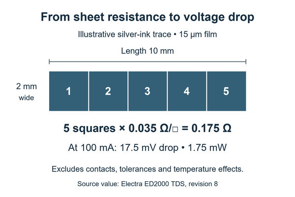
If the total allowed drop were 20 mV at that current, only 2.5 mV would remain for contacts and variation. That is a tight budget even though the nominal calculation appears to pass. Use the production resistance range and connection resistance before accepting the width.
To size the trace from a resistance limit, rearrange the same equation:
W ≥ Rs × L / Rmax
Here, Rmax is the resistance allowed for the printed strip after reserving a budget for its end connections. For a voltage-drop limit, start with Rtotal,max = Vmax / I. Use the qualified upper sheet resistance, maximum path length, and minimum finished width when allowing for manufacturing variation; a nominal calculation alone is not a released design limit.
The dissipation calculation is not a current rating. Temperature rise depends on the substrate, surrounding structure, duty cycle, and heat removal. Narrow necks, thickness variation, cracks, and connection interfaces can dominate the real result. When ink lies over a continuous copper path, that copper also changes the current distribution; measuring the combined path does not isolate the ink’s sheet resistance.
How Should Conductive Ink Features Be Designed on a PCB?
Define the finished ink feature and its relationship to copper, solder mask, and other printed layers. The fabricator needs more than a note saying “apply conductive ink.”
- Width and finished thickness: size the path from its resistance budget, then confirm the printer’s achievable geometry and variation. Specify whether width and thickness limits apply to the finished print, and include their permitted variation in the resistance budget.
- Copper overlap: provide enough overlap for electrical contact and registration tolerance. State which copper areas must remain covered after the maximum agreed misalignment, and check the worst-case overlay of both layers. There is no single overlap dimension suitable for every ink and supplier.
- Solder-mask transitions: discuss step height and coverage where ink crosses an edge. Electra’s ED5000-series technical guidance identifies trapped air under bridged ink at mask edges as a potential source of delamination during subsequent heating.
- Spacing and insulation: allow for print spread and registration between neighboring conductors. At a crossover, define the insulating layer’s extent and the isolation test; an unbroken top conductor does not prove the lower conductor is insulated.
- Contact and assembly areas: mark the mating surface, actuator footprint, and pads that must stay free of ink. If a contact surface is intentionally exposed, do not apply an overcoat that prevents it from functioning.
Also identify the actual substrate and surface finish beneath each printed region. Adhesion to bare laminate, copper, and solder mask can differ. For flexible constructions, agree on bend radius and cycling conditions before qualification rather than relying on a general “flexible” description.
For EBest Circuit’s carbon ink PCB service, submit the ink, copper, and solder-mask layers together with the finished-resistance requirement. Ask for the proposed print and registration tolerances before approving the artwork.
How Is Conductive Ink Printed and Cured on a PCB?
For conventional carbon ink PCB features, screen printing is a common deposition method. Dispensing and inkjet printing use different material and equipment requirements; a screen-printable paste cannot be assumed to work in either process.
- Prepare the surface. Follow the material’s cleaning instructions and confirm that the print area is clean and dry. Contamination or retained moisture can impair adhesion.
- Condition the ink. Check storage, shelf life, mixing, and permitted viscosity adjustment. Arbitrary thinning can change deposition and resistance.
- Print and inspect. Check a representative feature for registration, coverage, edge definition, and unintended bridges before continuing the batch.
- Apply the specified treatment. Record the required process conditions and confirm that the board and underlying layers tolerate them. Dry-to-touch does not prove complete cure or sintering.
- Measure the finished print. Check resistance and film condition against the agreed limits before later assembly operations.
Drying removes the liquid carrier; curing may develop binder properties; sintering develops connections between metallic particles in formulations designed for that process. Follow the specific technical and safety datasheets rather than a universal baking recipe.
What Problems Can Occur with Conductive Ink on a PCB?
Use the observed defect to choose the next check before changing the ink or process. Similar symptoms can have different causes.
- High or uneven resistance: check the actual width, finished thickness, coverage, cure record, and end connections. Compare an isolated process coupon with the product measurement. Control the identified source of variation rather than simply extending the bake.
- Lifting or delamination: inspect the failed interface for contamination, poor coverage across a mask edge, or incompatible processing. Correct preparation and layer compatibility, then repeat adhesion checks after the intended assembly heat exposure.
- Cracks or incomplete coverage: examine whether the defect follows a printed step, a thin region, or a flexed area. Adjust the geometry or qualified process and recheck both appearance and resistance under the relevant mechanical condition.
- Bridges or crossover shorts: compare the print with the registration limits and inspect the insulating layer. Correct spacing, print spread, or layer coverage as indicated, then test isolation as well as conductor continuity.
How Do You Test Conductive Ink Reliability?
Separate routine production inspection from qualification of the finished function. Agree on measurement conditions, sampling, acceptance limits, and permitted resistance change before comparing results.
- Production inspection: examine coverage, registration, bridges, and film damage; sample resistance at defined locations. Where thickness is critical, agree on a suitable measurement or cross-section method instead of estimating it from appearance.
- Low-resistance paths: use an appropriate four-wire setup to reduce lead and probe-contact error. Keep the test current, probe locations, temperature, and conditioning consistent between measurements.
- Contact and adhesion performance: test the actual mating contact at its specified force or travel and after the required operations. Verify film adhesion and function after relevant assembly heat exposure.
- Isolation and service stability: test neighboring nets and crossovers separately from conductor resistance. Include humidity, electrical bias, temperature, or flexing when they represent service risks, and compare before/after results.
A coupon can monitor the ink and print process, but cannot replace a contact assembly test. Retain the ink grade and batch, board revision, cure record, test geometry, and measured results so a change can be investigated.
What Should You Specify When Ordering a Conductive Ink PCB?
Specify the finished electrical function, its geometry, and how it will be accepted. A fabrication note saying only “carbon ink” leaves important material and process choices unresolved.
- Artwork and stack of features: provide a separate ink layer with copper and solder-mask references, substrate and finish, required coverage, and registration limits.
- Electrical and mechanical requirements: state resistance limits, measurement locations, current or voltage-drop budget where relevant, mating-contact conditions, assembly exposure, and operating environment.
- Material and acceptance: identify the required ink grade or request a proposed grade for approval. Include thickness requirements where necessary, test methods, sampling, quantity, and delivery target.
To review a carbon ink PCB design with EBest Circuit, send these requirements and the manufacturing files to sales@bestpcbs.com. Confirm the proposed ink, process limits, and acceptance tests before releasing the order.
FAQs About Conductive Ink for PCB
Q1: Is conductive ink the same as carbon ink?
A1: Carbon ink is one type of conductive ink. Silver, copper, and mixed-filler products are other options. A fabrication requirement should identify a grade or measurable performance limits, because even carbon formulations are not interchangeable.
Q2: Can components be soldered directly onto conductive ink?
A2: Only when the ink system specifies a compatible attachment process. Check the formulation, cure, solder alloy, and thermal exposure. Otherwise, use appropriate copper attachment pads or an explicitly qualified alternative connection.
Q3: How thick should the finished ink layer be?
A3: Use the thickness range qualified for the selected grade, geometry, and electrical target. Specify the finished dry or cured film, not wet deposit thickness. The 15 µm value in this article belongs to the cited example material; it is not a universal PCB requirement.
Q4: Should resistance always decrease after curing?
A4: The expected change depends on the formulation and process. Compare results after the specified treatment and conditioning. Unexpected resistance is a reason to check the print, connections, and cure record—not to assume that more heat will improve it.
Q5: Can conductive ink be printed over copper?
A5: Yes, with an ink and surface preparation qualified for that interface. Define overlap and any mask-edge transitions. When measuring, distinguish current through the copper from current through the ink or contact interface.