Printed circuit board terminology is the shared language used to describe a PCB from schematic capture through fabrication, assembly, inspection, and test. The words identify what the designer controls, what the manufacturer must build, which files carry the instructions, and what an inspection result actually proves.
Use each term in the context of its workflow stage and governing document. IPC-T-50N provides industry definitions, while the controlled drawing, procurement specification, and applicable product standard determine the requirement for a particular order.
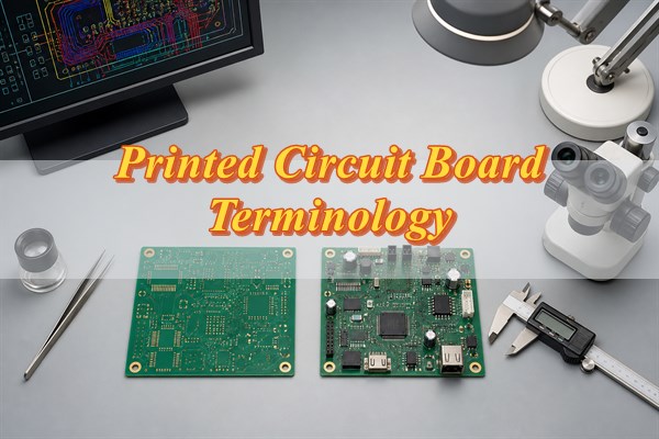
What Does Printed Circuit Board Terminology Cover?
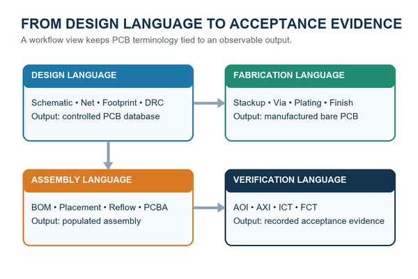
PCB terminology covers five connected layers of information: the electrical design, the physical layout, the manufactured bare board, the assembled board, and the evidence used to accept it. A term is most useful when you know both its definition and the decision it controls.
- Design terms describe intent: a schematic, net, footprint, clearance rule, and impedance constraint tell the CAD system what should connect and how the layout should behave.
- Construction terms specify the board: the stackup, core, prepreg, copper weight, via structure, finished thickness, and surface finish become purchasing and fabrication requirements.
- Manufacturing terms describe transformation: imaging, etching, lamination, drilling, plating, solder mask application, profiling, and electrical test turn the released data into a bare board.
- Assembly terms describe population: the BOM, pick-and-place data, stencil, solder paste, placement, reflow, and through-hole soldering convert the bare PCB into a PCBA.
- Inspection and test terms describe evidence: AOI, AXI, ICT, functional test, microsection, and impedance testing answer different questions and are not interchangeable proof.
The same word can also change meaning by context. A “layer” may mean a physical copper or dielectric layer, a CAD display layer, or a Gerber data layer. When a term affects cost, manufacturability, or acceptance, identify the object, units, revision, and governing document instead of relying on the label alone.
What Basic PCB Terms Describe the Board and Its Electrical Connections?
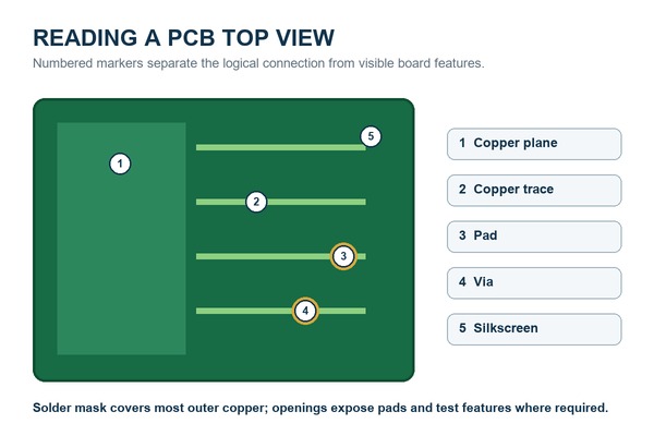
The basic PCB terms separate the unpopulated board from the assembled product and distinguish logical connections from physical copper. Getting this distinction right prevents an RFQ for a bare board from being mistaken for an assembly order.
- PCB or printed circuit board: the unpopulated interconnection structure made from insulating material, copper features, holes, protective coatings, and markings. IPC terminology may prefer “printed board” in formal usage, while PCB remains common in engineering and purchasing.
- PCBA or printed circuit board assembly: a PCB after specified electronic components have been attached. It normally requires component data and assembly instructions in addition to the bare-board package.
- PWB and PWA: printed wiring board and printed wiring assembly are established alternative or legacy terms. Confirm the supplier’s usage when a drawing or legacy program uses them.
- Schematic: the logical diagram of components and electrical connections. It states circuit intent but does not specify the physical routing or board geometry.
- Net: a named set of pins that must be electrically connected. A net is logical; one net may be implemented by several traces, copper pours, pads, and vias.
- Trace or track: a routed copper conductor on a signal layer. The two words are commonly used for the same physical feature, although local CAD terminology may prefer one.
- Plane: a broad conductive region used primarily for power or ground distribution. A plane may occupy most of a layer or share a mixed-signal layer with other features, so “plane layer” should not be assumed without checking the stackup and artwork.
- Reference designator: the unique identifier for a component, such as R15, C8, U3, or J2. It connects the schematic, BOM, assembly drawing, placement file, inspection program, and rework record.
Which PCB Design and Layout Terms Describe the Circuit Before Fabrication?
PCB design terminology converts circuit intent into physical objects and enforceable constraints. The designer should be able to trace each critical requirement from the schematic or constraint system to a visible feature and a checkable manufacturing output.
- Symbol and footprint: the symbol represents a part in the schematic; the footprint is its physical PCB representation. The footprint includes pads, outlines, reference text, courtyard or placement boundaries, and other assembly data.
- Land pattern: the complete arrangement of lands used to mount a component. In everyday CAD work, “footprint” and “land pattern” are often used together, but a footprint may contain more information than the solderable lands alone.
- Routing: the process of placing traces and vias to implement the net connections. Autorouting uses software algorithms; interactive routing keeps the designer in control of path and constraint decisions.
- Clearance: the permitted spacing between conductive features or other defined objects. State the object pair and applicable voltage/process rule because one global clearance value rarely covers every condition.
- Creepage: the shortest path along an insulating surface between conductive parts. It is a safety and insulation concept, not a synonym for the straight-line air distance called clearance in safety standards.
- Keepout: a defined region where specified objects may not be placed or routed. The blocked object classes matter: a copper keepout, component keepout, and routing keepout are different constraints.
- Copper pour or zone: an area filled with copper and assigned to a net, often ground or power. Its connection style, clearance, thermal relief, island removal, and layer determine its electrical and manufacturing behavior.
- Differential pair: two coupled conductors routed as a pair to carry complementary signals. Pair spacing, width, reference plane, dielectric geometry, skew, and discontinuities all affect performance.
- Controlled impedance: a requirement for a transmission structure to meet a target impedance within an agreed tolerance. The target alone is incomplete; the fabricator also needs the relevant layers, stackup, copper condition, geometry or impedance model, and coupon/test expectations.
- Microstrip and stripline: simplified transmission-line descriptions. A microstrip is routed next to a reference plane with air or coating on the other side; a stripline is embedded between reference planes. Real stackups may require a field solver rather than a generic equation.
- DRC or design rule check: a CAD check against defined design constraints, such as spacing, connectivity, width, hole size, or courtyard rules. A clean DRC proves conformance to the loaded rules, not that those rules match the selected factory’s process.
CAD systems may use different names for similar objects. Review the released data by function: confirm which objects carry connectivity, copper geometry, mask openings, component identity, mechanical limits, and manufacturing constraints.
How Do PCB Stackup and Material Terms Describe Board Construction?
PCB material terminology defines the insulating system, copper arrangement, thickness, and electrical or thermal properties of the finished board. A material family name such as FR-4 is a starting point, not a complete laminate specification.
- Stackup: the ordered construction of copper and dielectric layers, including layer functions, material types, thicknesses, and copper weights. It links impedance, manufacturability, thickness, thermal behavior, and cost.
- Core: a cured dielectric sheet, commonly copper clad on one or both sides before processing. In a multilayer build it provides dimensional structure between copper layers.
- Prepreg: resin-impregnated reinforcement that is not fully cured before lamination. Heat and pressure cause it to flow, fill, and bond the multilayer stack.
- Copper-clad laminate: dielectric material supplied with copper foil bonded to it. The laminate grade and copper foil type should match the electrical, thermal, mechanical, and regulatory requirements.
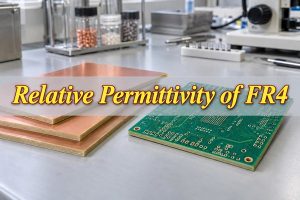
- FR-4: a broad family of flame-retardant glass-reinforced epoxy laminates. Different FR-4 grades can have different thermal and electrical behavior, so a purchasing document may need a named grade or a bounded equivalent.
- Tg, glass transition temperature: a material transition region associated with a marked change in mechanical behavior. The value depends on the stated test method and does not by itself establish high-temperature reliability.
- Td, decomposition temperature: a test-defined temperature at which a specified mass loss occurs. It describes a different mechanism from Tg and should not be substituted for it.
- CTE, coefficient of thermal expansion: the rate of dimensional change with temperature in a stated direction and range. Z-axis expansion is especially relevant to plated-hole stress during thermal excursions.
- Dk and Df: dielectric constant and dissipation factor, respectively. Values depend on frequency, test method, resin content, construction, and material condition; use compatible data when modeling impedance or loss.
- Copper weight: a mass-per-area convention used to describe nominal copper foil or plating build. For a released board, state whether the value refers to starting foil, finished copper, an inner layer, or an outer layer.
- Finished thickness: the final board thickness after lamination and surface processing, normally with a tolerance. It is not simply the arithmetic total of nominal raw sheets.
What Do Pad, Land, Via, and Hole Terms Mean?
Pads and lands provide component or test interfaces, while vias and plated holes create vertical or lead-bearing connections through the board. The terms overlap in casual speech, but their functions and manufacturing controls differ.
- Pad: a CAD copper object used for a component terminal, test point, via, or mechanical feature. Its type, layers, opening, drill, and net assignment determine its role.
- Land: the conductive pattern intended for a component terminal. “Land pattern” refers to the complete mounting pattern; a CAD library may call each individual land a pad.
- Annular ring: the copper remaining around a drilled hole on a particular layer. Finished-hole size, drill position, pad size, plating, and breakout criteria affect the result.
- PTH or plated through-hole: a hole with conductive plating that connects selected layers. It may accept a component lead or act as an interconnect feature.
- NPTH or non-plated through-hole: a hole without conductive wall plating, often used for mounting, alignment, or mechanical clearance. Copper clearances and fabrication drawing identification help prevent unintended plating.
- Through via: an interconnect that extends from one outer surface to the other, even if its net only uses some of the traversed layers.
- Blind via: an interconnect from an outer layer to one or more inner layers without reaching the opposite outer surface.
- Buried via: an interconnect between inner layers that is not visible on either finished outer surface.
- Microvia: a small blind or buried structure formed by a microvia process, commonly laser drilling. Its layer span, stacking or staggering, fill, capture pads, and reliability requirements must be defined; “microvia” is not merely a nickname for any small mechanical drill.
- Via-in-pad: a via placed in a component land. The assembly process may require filling, planarization, and capping so the pad remains solderable and does not draw solder into the hole.
- Aspect ratio: a depth-to-diameter relationship used to judge drilling and plating feasibility. Confirm which depth and diameter definitions the manufacturer applies to the specific through, blind, or microvia process.
What PCB Manufacturing Terms Appear in a Fabrication Quote?
PCB manufacturing terminology describes both the process used to build the bare board and the features that must appear on the finished product. Quote data should describe the required result; the fabricator selects the controlled process unless the design specifically constrains it.
- DFM, design for manufacturability: a review of released design data against a manufacturer’s process capabilities and risk rules. It complements DRC by applying the actual factory’s processes in addition to the CAD constraints.
- CAM, computer-aided manufacturing: preparation of design data for imaging, drilling, routing, testing, panelization, and other production operations. CAM edits should be documented and approved when they change design intent.
- Imaging and etching: imaging transfers the conductor pattern to a process layer; etching removes unwanted copper. The resulting conductor width and spacing depend on the production process and copper build.
- Lamination: heat and pressure bond cores, prepregs, and copper into a multilayer structure. Sequential lamination adds additional build cycles for some blind, buried, or stacked interconnect structures.
- Desmear: treatment that removes resin residue and conditions drilled hole walls before metallization. It supports reliable contact between hole plating and internal copper.
- Copper plating: deposition of copper on hole walls and selected surfaces. Drawings should distinguish minimum finished copper requirements from starting foil when that distinction matters.
- Solder mask or solder resist: the patterned protective polymer coating over most finished copper. Mask openings expose pads and other features intended for finish, soldering, contact, or test.
- Legend or silkscreen: visible markings such as reference designators, polarity indicators, part numbers, and logos. Modern legends may be printed by several methods even though “silkscreen” remains the common name.
- Surface finish: the final coating on exposed copper, selected for solderability, contact function, shelf handling, flatness, wire bonding, wear, or other project needs. HASL, ENIG, ENEPIG, OSP, immersion silver, immersion tin, and hard gold are not interchangeable selections.
- Panelization: arrangement of one or more board images within a manufacturing or assembly panel. Rails, tooling holes, fiducials, coupons, breakaway tabs, routing gaps, and assembly handling requirements affect the panel definition.
- V-score and routing: two common methods used to create separable board outlines. V-scoring leaves a controlled web along straight score lines; routing cuts the profile with a tool and can support irregular shapes and tab features.
- Test coupon: a structure placed on a production panel to evaluate a controlled property such as impedance, plating, material behavior, or process integrity. A coupon is useful only when its design and test method represent the product requirement.
How Do PCB Files and Documentation Transfer a Design to Manufacturing?
Manufacturing files divide into image or product-model data, drill and mechanical data, component data, drawings, and revision-controlled notes. No file name proves completeness; open the released package in an independent viewer and compare it with the approved source design.
- Gerber: the industry-standard layer-image format maintained by Ucamco for PCB fabrication data. The official Gerber format resource publishes the layer and job specifications, while drill data is commonly supplied separately in an NC drill format. Attributes and a Gerber job file can add context, but the exporter and release package determine what is actually present.
- NC drill or Excellon file: machine-readable hole locations, sizes, and tool information. Separate plated/non-plated files or explicit attributes help prevent hole-type ambiguity.
- Fabrication drawing: the controlled drawing for outline dimensions, stackup or construction references, finished thickness, hole tables, tolerances, finish, marking, impedance, special processes, standards, and notes not fully expressed by artwork.
- Netlist: a connectivity representation used to compare intended electrical connections with manufactured artwork or test data. It does not replace geometry or a functional test plan.
- ODB++: a structured PCB product-model format that can contain fabrication, assembly, and test information in one job hierarchy. The ODB++Design resource describes the format; the recipient should still confirm the supported version and expected contents.
- IPC-2581: an open standard for PCB design and manufacturing data exchange. The IPC-2581 Consortium provides format information and viewers; exporter settings and recipient compatibility still require verification.
- BOM, bill of materials: the controlled list of components and purchasing information for assembly. Useful fields include reference designators, manufacturer, manufacturer part number, quantity, approved alternatives, and DNP/variant status.
- Centroid or pick-and-place file: component reference, position, rotation, and board side data used to prepare placement programs. Origin, units, rotation convention, bottom-side transformation, and variant scope must agree with the assembly drawing.
- Assembly drawing: the visual and note-based definition of component locations, orientation, polarity, mechanical hardware, special soldering, adhesive, coating, and variant requirements.
A reliable release uses one revision identity across the PCB database, artwork or product model, drawing, BOM, placement file, and assembly notes. A correct file from the wrong revision is still an incorrect manufacturing package.
What PCB Assembly and Soldering Terms Describe PCBA Production?
PCB assembly terminology describes how components are prepared, placed, soldered, cleaned, protected, and tracked on the bare board. It also distinguishes a component package from the production method used to attach it.
- SMT and SMD: surface-mount technology is the assembly method; a surface-mount device is a component intended for surface mounting. Calling a production line “SMD” may be common speech, but SMT is the process term.
- THT: through-hole technology inserts component leads through holes and solders them on the opposite side or within the plated barrel. Mixed-technology assemblies can use both SMT and THT.
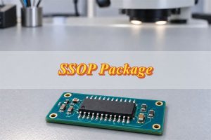
- Package: the physical component form, such as QFN, QFP, BGA, SOIC, or a chip passive size. Package name alone may not specify lead pitch, body size, height, thermal pad, or land pattern.
- Pitch: center-to-center spacing of repeated terminals or features. State the object and units because connector pitch, BGA pitch, lead pitch, and trace pitch describe different geometries.
- Solder paste: a controlled mixture containing solder alloy particles and flux system, deposited on pads before surface-mount placement. Alloy, powder classification, flux chemistry, storage, stencil transfer, and reflow profile influence performance.
- Stencil and aperture: the stencil is the patterned foil or screen used to print solder paste; each aperture controls where and how much paste is deposited. Aperture design may differ from the copper land geometry.
- Fiducial: an optical reference mark used by assembly equipment to correct board or local component position. Global and local fiducials serve different alignment scopes.
- Pick and place: automated component placement using BOM and coordinate data, feeder setup, machine vision, and programmed orientation. A placement result still requires polarity and first-article verification.
- Reflow soldering: a thermal process that melts deposited solder paste and forms surface-mount joints. The profile is developed for the assembly, materials, component limits, thermal mass, and process window.
- Wave and selective soldering: wave soldering exposes a broad underside region to a solder wave; selective soldering targets chosen through-hole locations with controlled tooling or a localized wave.
- DNP or DNI: do not populate/do not install. The assembly data should identify the affected references and variant so omitted parts are intentional rather than missing.
- Conformal coating: a protective coating applied to specified areas of an assembled board. Material, masking, coverage, thickness, cure, inspection, and keepout requirements belong in controlled assembly documentation.
How Do PCB Inspection and Testing Terms Describe Verification?
Inspection observes attributes, while testing applies a defined stimulus or measurement to verify a requirement. Each method has a limited fault model, so “tested” is incomplete unless the method, coverage, limits, and acceptance criteria are identified.
- SPI, solder paste inspection: measures or evaluates printed paste before placement. It can detect deposit-volume, area, height, offset, and bridging risks within the programmed limits.
- AOI, automated optical inspection: uses cameras and image-processing rules to inspect visible features. On assemblies it can check placement, polarity, solder appearance, and component presence, but hidden joints remain outside direct optical view.
- AXI or automated X-ray inspection: uses X-ray imaging for hidden or internal structures such as BGA joints, voiding, and some through-hole fill conditions. A programmed criterion and suitable image geometry are still required.
- Bare-board electrical test: checks manufactured conductor continuity and isolation against test data. Flying-probe systems use movable probes; fixture tests use dedicated contacts. Neither proves that an assembled circuit performs its intended function.
- ICT, in-circuit test: accesses nets or component nodes on an assembly to test connectivity, selected component values, orientation, shorts, opens, and other programmed conditions. Coverage depends on access, fixture or probe strategy, and the test program.
- FCT, functional circuit test: powers or stimulates the assembly and checks defined outputs or behavior. Its value depends on realistic interfaces, limits, loads, firmware state, calibration, and recorded results.
- Boundary scan: a standards-based digital test method that uses compatible integrated circuits and a test access port to exercise interconnects and devices. It can improve coverage where physical probe access is limited.
- Microsection: a prepared cross-section examined to evaluate internal board structures such as plating, interfaces, layer registration, dielectric spacing, and hole quality. The sampling plan and acceptance criteria determine what the result represents.
- Impedance test: measurement of specified coupon or product structures against target and tolerance. The result should identify the structure, layer, method, frequency assumptions where relevant, and disposition of out-of-limit data.
Standards also have distinct roles. IPC describes IPC-A-600 as acceptability guidance for bare printed boards, IPC-A-610 as acceptability criteria for electronic assemblies, J-STD-001 as requirements for soldered assemblies, and IPC-6012 as a qualification and performance specification for rigid printed boards. A drawing should identify the applicable document and revision instead of using “IPC compliant” as a universal requirement.
Which PCB Terms Are Commonly Confused?
The most expensive terminology errors occur when two related words control different deliverables or acceptance decisions. Use the distinction column below to decide what to specify or verify next.
| Terms | Engineering Distinction | Next Check |
|---|---|---|
| PCB / PCBA | Bare interconnection board / board populated with components | Confirm whether the quote includes component sourcing and assembly |
| Pad / Land / Footprint | CAD copper object / component terminal area / complete physical library representation | Compare the package drawing, land pattern, mask and paste openings |
| Net / Trace / Plane | Logical connection / routed conductor / broad conductive region | Verify net assignment, physical path and reference structure |
| Via / Component Hole | Layer interconnect / hole intended to accept a lead or terminal | Check finished-hole size, plating, pad geometry and assembly use |
| Solder Mask / Paste Mask | Permanent board coating / stencil-aperture data for paste deposition | Review mask expansion and paste-aperture reductions separately |
| Silkscreen / Assembly Drawing | Marking printed on the board / controlled document defining assembly | Do not rely on board legend for all orientation or process instructions |
| DRC / DFM | CAD-rule conformance / factory-process manufacturability review | Confirm the CAD rules match the selected process capabilities |
| Electrical Test / Functional Test | Bare-board continuity/isolation / powered assembly behavior | Specify separate test data, limits, and evidence for each stage |
How Do These PCB Terms Connect During a Real Release?
A reliable release connects every design decision to a manufacturing artifact and a checkable output. Do not advance the package until the observable result from the current step is available and tied to the same revision.
- Lock the schematic and connectivity. Confirm the component references, net names, pin mapping, variants, and electrical rules; the observable result is an approved schematic/netlist revision.
- Assign verified footprints and stackup constraints. Match packages to land patterns and specify layer functions, materials, thickness, copper, via structures, and impedance needs; the observable result is a controlled PCB database with a reviewable stackup.
- Complete layout and rule checks. Route nets, place planes and keepouts, verify spacing and mechanical interfaces, then review DRC exceptions; the observable result is a clean or formally waived constraint report.
- Generate one revision-controlled manufacturing package. Export the selected fabrication format, drill/mechanical data, drawings, BOM, centroid data, assembly instructions, and test information; the observable result is one named release whose files share the same revision.
- Review the exported data independently. Open artwork or product-model data in a separate viewer and compare outline, layers, holes, nets, mask, legend, component data, units, and origin with the source; the observable result is a signed release review or recorded discrepancy list.
- Resolve DFM and assembly questions before build. Evaluate manufacturability changes against design intent and update the controlled source when required; the observable result is an approved question log and a final buildable revision.
- Match inspection evidence to the requirement. Collect bare-board test, impedance, inspection, assembly, and functional records specified for the order; the observable result is traceable evidence that answers the defined acceptance questions.
What PCB Abbreviations Should You Recognize Quickly?
Read a PCB abbreviation together with the workflow stage it controls. The same short label can otherwise be mistaken for a product, process, file, inspection method, or acceptance result.
| Abbreviation | Full Term | Workflow Role |
|---|---|---|
| PCB | Printed Circuit Board | Unpopulated manufactured board |
| PCBA | Printed Circuit Board Assembly | Board with specified components installed |
| CAD | Computer-Aided Design | Creates schematic and layout data |
| CAM | Computer-Aided Manufacturing | Prepares production data and programs |
| DRC | Design Rule Check | Verifies the PCB against loaded CAD rules |
| DFM | Design for Manufacturability | Checks fit with a production process |
| BOM | Bill of Materials | Controls assembly component identity and quantity |
| SMT | Surface-Mount Technology | Places and solders surface-mount devices |
| THT | Through-Hole Technology | Installs leaded parts through board holes |
| PTH | Plated Through-Hole | Conductive hole through the board |
| NPTH | Non-Plated Through-Hole | Mechanical or nonconductive hole |
| SPI | Solder Paste Inspection | Checks paste deposits before placement |
| AOI | Automated Optical Inspection | Checks visible programmed features |
| AXI | Automated X-Ray Inspection | Examines hidden solder or internal features |
| ICT | In-Circuit Test | Tests accessible assembly nodes and components |
| FCT | Functional Circuit Test | Verifies defined powered behavior |
What Should You Specify Before Requesting a PCB or PCBA Quote?
A quote-ready package identifies the product stage, board construction, critical features, assembly scope, test expectations, and one controlled revision. The manufacturer can then separate assumptions from confirmed requirements before price or build decisions are made.
- Product and revision: state whether the request is PCB fabrication, assembly, or both; provide part number, revision, quantity, panel preference, and approved source package.
- Board construction: specify layer count and order, material or approved-equivalent boundary, finished thickness, copper requirements, via structures, minimum features, controlled impedance, and any special mechanical or thermal construction.
- Fabrication finish: specify solder mask and legend requirements, exposed-copper surface finish, edge contacts, via fill/cover requirements, marking, profile, and acceptance or performance documents with revisions where applicable.
- Assembly data: provide a revision-matched BOM, pick-and-place file, assembly drawing, polarity and variant information, DNP list, stencil or paste requirements when controlled by the customer, and special handling/coating instructions.
- Inspection and test: identify bare-board electrical test, impedance evidence, assembly inspection, ICT/FCT, programming, serialization, traceability, report format, sampling, and acceptance limits that the order actually requires.
- Open assumptions: ask the supplier to list substitutions, stackup proposals, panel changes, CAM adjustments, test limitations, and missing data before release. Close the question log against the final revision rather than approving changes only in email fragments.
FAQs About PCB Terminology
Q1: Why should an RFQ distinguish PCB fabrication from PCBA?
A1: PCB fabrication produces the unpopulated board; PCBA adds component sourcing, placement, soldering, inspection, and any specified powered test. State the required product stage so the quotation includes the correct data, materials, labor, and acceptance evidence.
Q2: How should a team handle PWB or PWA terms in legacy documents?
A2: Preserve the controlled drawing’s wording until its intended product state is confirmed. Map PWB to the bare interconnection product and PWA to the populated assembly only when the program owner, cited standard, and release documents support that interpretation.
Q3: Can a footprint and a land pattern be treated as the same deliverable?
A3: Not automatically. A land pattern defines the conductive mounting lands, while a CAD footprint may also include mask and paste openings, assembly outlines, courtyard limits, reference text, and 3D or placement data. Review all of those objects against the component package drawing.
Q4: Does FR-4 identify the exact PCB material?
A4: No. FR-4 covers a broad family of flame-retardant glass-reinforced epoxy laminates. When thermal, loss, CAF, halogen, regulatory, or impedance behavior matters, specify a named material or bounded equivalent properties with compatible test methods.
Q5: What information must accompany a controlled-impedance requirement?
A5: Identify the target and tolerance, signal structure, layer or layer pair, reference plane, stackup, copper condition, and coupon or product-test expectation. The impedance value alone does not tell the fabricator which geometry or construction must meet it.
Q6: Does “IPC Class 3” completely define board and assembly acceptance?
A6: No. Tie the class to the applicable product or assembly standard, document revision, product type, controlled drawings, and procurement requirements. Bare-board performance, bare-board acceptability, soldering process requirements, and assembly acceptability belong to different documents.
Q7: Can one manufacturing file format replace the complete release package?
A7: No file name proves completeness. Gerber, ODB++, or IPC-2581 data may carry much of the product definition, but drawings, BOM and placement data, variants, material notes, test requirements, and revision identity must still be checked against the recipient’s supported workflow.
Q8: Which inspection result proves that an assembled board works?
A8: No inspection image proves complete circuit function. AOI checks programmed visible features, AXI examines selected hidden structures, ICT tests accessible nets or components, and FCT verifies defined powered behavior. Acceptance requires the method whose fault coverage matches the stated requirement.
How Can You Use PCB Terminology More Reliably?
Reliable printed circuit board terminology ties each word to a controlled object, product state, document, or test result. Add the missing qualifier when a label is ambiguous: bare-board electrical test, assembled-board functional test, CAD clearance, finished conductor spacing, starting copper, or finished copper.
Keep one part number and revision across the design and manufacturing package, review exports independently, record approved deviations, and confirm what each inspection method can and cannot detect. This makes communication shorter while preserving the engineering detail needed for quotation, production, and acceptance.
If you want a manufacturing review of a revision-controlled PCB or PCBA package, send the stackup, fabrication data, BOM, placement files, drawings, and test requirements to sales@bestpcbs.com. Ask for a documented list of missing inputs and manufacturability questions before production.