LVDS PCB example designs are useful when the stackup, pair geometry, routing decisions, termination, and test plan describe one coherent channel. This worked design case follows a single 75 mm point-to-point lane on a four-layer board with a nominal 100Ω differential target. It also marks the values that must be confirmed by the selected fabricator, so an illustrative number is never mistaken for a production release value.
What Does This LVDS PCB Example Demonstrate?
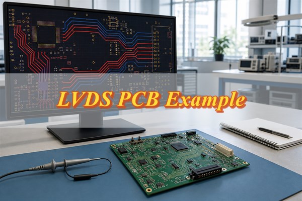
This LVDS PCB example demonstrates the complete decision chain for one controlled-impedance lane. One driver connects to one receiver with no branches. The pair remains on L1 over continuous L2 ground, uses no signal vias, and ends at a receiver-side parallel termination. These choices remove avoidable discontinuities and make later TDR events easier to correlate with the physical route.
A nominal 3.5 mA through a 100Ω termination produces about 350 mV of differential voltage. The receiver detects the voltage difference between P and N, so equal treatment of the two conductors helps preserve common-mode rejection. Unequal escapes, connector pins, vias, or reference paths convert part of a common disturbance into differential error. This is why symmetry is an electrical requirement rather than a cosmetic layout preference.
The reusable output is not a copied width-and-gap pair. It is a release package in which the device requirements, manufactured stackup, field-solved geometry, CAD rules, fabrication note, and acceptance evidence all carry the same revision.
What Parameters Are Used in This 100Ω LVDS PCB Example?
The example fixes the channel topology and routing choices first, while leaving production-dependent geometry open until the stackup is approved. The table distinguishes a chosen design value from a value that still requires fabricator or device confirmation.
| Parameter | Worked-example value |
| Topology | One driver to one receiver |
| PCB layers | Four layers |
| Routing and reference layers | L1 microstrip over L2 ground |
| Provisional L1-to-L2 dielectric | 0.18 mm |
| Provisional finished outer copper | 35 μm |
| Trace width and pair spacing | Pending production-stackup approval |
| Differential impedance | 100Ω nominal |
| Route length and P/N mismatch | About 75 mm; 0.25 mm or less |
| Signal-via count | Zero |
| Termination | 100Ω, 1%, at the receiver |
| Verification | Solver record, same-panel coupon TDR, and powered-channel eye test as required |
The 0.18 mm dielectric and 35 μm copper values are provisional inputs, not universal production dimensions. Replace them with the fabricator’s pressed dielectric and finished-copper values, then solve the trace width and spacing for the selected laminate, solder mask, and etch process. Confirm the impedance tolerance and skew limit against the chosen devices before the layout is approved.
How Is the 4-Layer Stackup Designed for the LVDS Pair?
The example keeps the pair on L1 because the adjacent L2 ground plane provides an unambiguous return path without a signal-via transition. L3 carries power behind the reference plane, while L4 remains available for lower-speed routing and ground copper. The choice simplifies correlation between the straight pair, coupon, and measured impedance.
| Layer or construction item | Role in the example |
| L1 | Components and LVDS microstrip pair |
| L1-L2 dielectric | Primary height controlling the microstrip field |
| L2 | Continuous ground reference |
| L3 | Power distribution behind the L2 reference plane |
| L4 | Lower-speed signals and ground copper |
The provisional 0.18 mm dielectric and 35 μm finished copper are enough to begin a discussion, but they do not identify a complete producible construction. The fabricator still needs the laminate family, glass/resin construction, relevant design Dk, solder-mask model, and etch assumptions. This is the same release discipline used for controlled impedance circuit boards: approve the stackup and geometry together, then lock the CAD rule to that revision.
What Trace Width and Spacing Produce 100Ω Differential Impedance?
No defensible final W/S can be stated from impedance target and board layer count alone. Width, pair spacing, finished copper, dielectric height and Dk, solder mask, and nearby copper all change the differential impedance. Copying a 5 mil width and 5 mil gap from another four-layer board can therefore miss 100Ω.
The geometry becomes reproducible when the calculation and approval trail is reproducible:
- Freeze the electrical requirement. Record the selected driver and receiver, nominal differential impedance, permitted tolerance, line rate, output edge rate, and termination mode. The result is a constraint sheet tied to actual part numbers.
- Freeze the candidate construction. Obtain the proposed laminate build, pressed dielectric height, finished copper, solder-mask condition, and relevant dielectric data. The result is a named stackup revision rather than a generic “four-layer FR-4” description.
- Solve a manufacturable geometry. Use a field solver or the fabricator’s impedance tool with the finished construction. Compare at least one practical W/S alternative so the selected pair is not sitting unnecessarily close to a line or spacing limit.
- Return the result to layout. Enter the approved width, gap, target, and tolerance into the differential-pair rule. Re-run the impedance calculation if the layer, copper, dielectric, mask, or adjacent-copper environment changes.
- Close the manufacturing loop. Put the released geometry and controlled net class in the fabrication package, then require the agreed coupon and report. A solver screenshot without the matching production stackup is not final evidence.
The Analog Devices LVDS application note explains the 100Ω transmission-line and termination behavior. It does not turn any one layout geometry into a universal recipe. In this example, the honest final result is therefore “100Ω target, production W/S pending stackup confirmation” until a traceable solver or fabricator record is available.
How Is the LVDS Pair Routed from Driver to Receiver?
The 75 mm lane is routed as one continuous coupled structure on L1, with zero signal vias and constant geometry over L2 ground. This reduces the number of variables that can create an impedance step and makes the route easier to review, fabricate, and diagnose.
- Place the endpoints for a direct corridor. Orient the driver and receiver so their P/N pins face a practical routing channel. The visible result is a route with no branch and no forced neck-down.
- Apply the approved pair rule. Assign the fabricator-confirmed width and spacing to the complete lane. A rule report should show one controlled definition rather than hand-edited segments.
- Match the two escapes. Give P and N comparable pad exits, bends, and local copper. The layout review should reveal no detour applied to only one conductor.
- Preserve the reference plane. Inspect L2 below every segment, including package and connector keepouts. A solid reference is more valuable than a visually perfect serpentine over a plane gap.
- Correct mismatch near its source. Add compact tuning only when the measured electrical-length difference needs it. The final report should meet the device-derived skew budget without a large coupled meander.
- Check aggressor spacing. Review clocks, switching nodes, and neighboring pairs against the project’s crosstalk target. Use simulation when density or long parallel exposure makes a simple spacing heuristic uncertain.
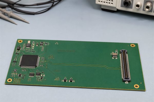
Texas Instruments’ high-speed layout guidance for LVDS serializers and deserializers also emphasizes controlled differential impedance, continuous reference planes, symmetric pair geometry, and minimal stubs and vias. Numerical tolerances in any device guide remain application-specific unless the selected parts adopt them.
Where Should the LVDS Termination Resistor Be Placed?
For this point-to-point lane, place the external 100Ω parallel termination at the receiver pins and keep the final connection as short and symmetric as possible. Review the complete pad-to-pin path rather than judging placement by the schematic symbol alone.
- Confirm whether termination is already inside the receiver. Some receivers provide integrated 100Ω termination, as shown in the Microchip LVDS receiver overview. An enabled internal 100Ω path in parallel with an external 100Ω resistor creates about 50Ω, which increases loading and reduces differential amplitude.
- Keep the resistor-to-pin connection short. A long segment beyond the resistor acts as a stub after the matched load. Inspect both P and N connections and remove unequal detours, neck-downs, or pad exits.
- Use the specified resistor value and tolerance. A 1% part controls component variation, but it cannot repair a poor connector launch, long pad stub, or incorrectly designed trace impedance.
- Record the populated option. Make the schematic, BOM, assembly data, and receiver configuration agree on internal or external termination so the assembled channel matches the reviewed design.
How Should Vias, Connectors, and ESD Protection Be Handled?
Every unavoidable discontinuity should be symmetric, modeled or measured when necessary, and provided with a continuous return path. The worked route uses zero signal vias, but a real product may need a connector, ESD network, or layer transition. Those structures must be treated as part of the channel.
- Differential vias: use the same drill, pad, antipad, and layer span for P and N. Add nearby ground stitching vias when return current changes reference layers, then inspect the transition in cross-section or 3D.
- Connectors: assign adjacent, symmetric differential pins with nearby grounds where the connector family permits. Include the launch, connector, and cable models when the link crosses between boards.
- ESD devices: select a part whose capacitance and bandwidth suit the actual line rate. Route through a symmetric footprint with short connections and compare the channel with and without the device if eye margin is limited.
- Test access: avoid open-ended pad branches. Use a characterized probe arrangement or connector, and include its capacitance and stub length in the measurement plan.
The Renesas LVDS and MIPI board design guide reinforces short routing, gentle turns, mirrored transitions, nearby ground vias, and continuous reference ground. The layout decision is complete only when the return path is reviewed with the signal path.
What Should Be Specified for Controlled-Impedance PCB Manufacturing?
The fabrication package should connect the electrical target to a named construction and an acceptance record. It should not freeze a borrowed W/S pair before the fabricator confirms how that pair will be built.
| Fabrication item | What to state |
| Controlled net class | 100Ω differential for the named LVDS pair or class |
| Tolerance | Device- and project-approved tolerance agreed with the fabricator |
| Routing structure | L1 microstrip referenced to L2 ground for this example |
| Released geometry | Approved finished trace width and pair spacing |
| Permitted tuning | Whether width, gap, or dielectric thickness may be adjusted |
| Material control | Laminate family, construction, finished copper, and relevant dielectric data |
| Coupon and report | Same-panel differential coupon and TDR report when required |
The Polar Instruments controlled-impedance guide explains why designer and fabricator must agree which dimensions may be adjusted and why a representative coupon should follow the production construction. This handoff prevents a silent material or geometry change from invalidating the CAD result.
How Are TDR and Eye Diagram Tests Used to Verify the LVDS Channel?
TDR verifies impedance behavior; the eye diagram verifies the powered channel at its operating conditions. The two tests answer different questions and should not be used as substitutes for each other.
- Measure the bare-board coupon. Calibrate the differential TDR setup and compare the stable region with the released target and tolerance. The report should identify the order, panel, coupon construction, launch, and measurement limits.
- Map discontinuities to distance. Correlate abrupt TDR events with connector launches, via fields, pads, or geometry changes. A local excursion does not automatically mean the entire straight trace has the wrong W/S.
- Power the intended channel. Record the transmitter settings, receiver load, data pattern, data rate, connector or cable, test point, and fixture. Reproducibility depends on these conditions.
- Apply a measurable eye criterion. Compare eye height, eye width, jitter, and mask margin with the device or system requirement. “Looks open” is an observation, not an acceptance limit.
- Correlate the results. If the coupon passes but the eye fails, investigate packages, termination, connectors, vias, crosstalk, power noise, and fixture de-embedding before changing the straight-line geometry.
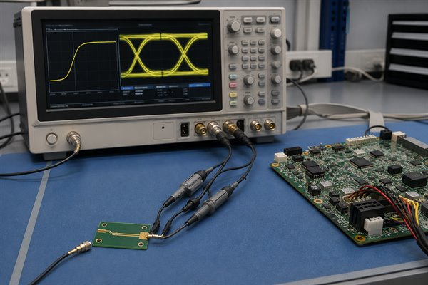
A real TDR value should be published only with its target, tolerance, coupon construction, test setup, and traceable report. The conceptual image above illustrates the verification stage; it is not a production measurement or first-hand test record.
How Do You Diagnose Common LVDS Signal Integrity Problems?
Start with the observed failure, then select the test that can separate geometry, termination, timing, loss, and process variation. This keeps troubleshooting from repeating the routing rules without identifying the next decision.
- TDR plateau remains above the target: the produced geometry or dielectric environment may be raising impedance. Compare the measured coupon dimensions, pressed dielectric, finished copper, solder mask, and solver inputs with the approved stackup.
- Ringing repeatedly appears after one transition: a launch, pad, via, connector, or termination discontinuity may be reflecting energy. Map the TDR distance to the physical route, then confirm the populated termination state.
- The eye closes horizontally: skew, jitter, crosstalk, or data-dependent loss may be reducing timing margin. Compare P/N electrical delay, transmitter clocking, aggressor activity, and channel loss at the operating data rate.
- The eye closes vertically: attenuation, overtermination, power noise, or probe loading may be reducing amplitude. Verify internal and external termination, connector loss, supply noise, and fixture loading.
- Common-mode radiation increases: P/N asymmetry or a broken reference path may be converting common-mode energy. Inspect unequal escapes, vias, connector pins, pad stubs, plane gaps, and spacing changes.
- Only one panel fails coupon TDR: material, etch, plating, registration, or panel-position variation may be involved. Compare coupon traces, stackup records, microsections, and panel position before changing the PCB design.
A geometrically length-matched pair can still fail over a plane gap, and a small mismatch may be acceptable when it stays within the receiver’s skew budget. The diagnosis should follow the measured failure mechanism, not whichever layout metric is easiest to display.
How Do You Verify an LVDS PCB Design Before Fabrication?
Verify that the device limits, stackup, CAD rules, fabrication notes, and test plan all describe the same LVDS channel. A final review should connect each design choice to a drawing, rule, report, or measurable acceptance criterion.
- Confirm the device limits. Record the exact driver and receiver data-sheet revisions, supported line rate, impedance guidance, termination mode, and skew budget. These values define the electrical limits the PCB must support.
- Approve the stackup and W/S together. Obtain the fabricator’s construction, material data, finished copper, solver result, producible width and spacing, and quoted impedance tolerance. The final CAD rule should match that approved revision.
- Inspect the implemented route. Confirm the pair uses the approved layer, width, spacing, target, and tolerance without a local override or neck-down. Review the entire L2 reference path and compare P/N escapes, bends, pads, transitions, and tuning.
- Check connectivity and termination. Verify P-to-P and N-to-N through every pin, connector, and net rename. Make the schematic, BOM, assembly drawing, and receiver setting agree on internal or external termination.
- Define fabrication verification. State the controlled net class, impedance target and tolerance, representative coupon construction, TDR method, and report requirement. This gives the fabricator an acceptance target tied to the actual stackup.
- Define the powered-channel test. Specify the data rate, pattern, test point, fixture, relevant operating corners, and measurable eye or jitter criteria. The resulting test should show whether the assembled channel meets the system requirement.
For a long or discontinuity-heavy channel, add pre-layout and post-layout simulation using actual package, connector, via, and cable models where available. Correlate the first physical measurements with the model so the next revision addresses a known mechanism rather than a generic “high-speed” concern.
FAQs About LVDS PCB Example
Q1: Can LVDS traces be routed on an inner layer?
A1: Yes. An inner-layer stripline can provide strong field containment, but it normally adds escape vias and makes probing harder. Choose it when routing density, shielding, or reference continuity outweighs the transition cost, then solve the impedance for the actual two-plane geometry.
Q2: Should LVDS use microstrip or stripline routing?
A2: Use the structure that gives the cleanest reference path and a manufacturable 100Ω geometry for the whole channel. Microstrip simplifies access and can avoid vias; stripline offers more shielding but changes loss, coupling, and transition requirements. Compare the complete route, not the straight segment alone.
Q3: How far should an LVDS pair be from other high-speed signals?
A3: There is no universal spacing that fits every stackup and parallel run length. Start with a conservative separation rule, then check the nearest aggressor’s edge rate, coupling length, layer relationship, and allowable crosstalk. Use simulation when density forces long, close parallel exposure.
Q4: Does solder mask affect 100Ω differential impedance?
A4: Yes. Solder mask changes the dielectric environment around an outer-layer pair and can shift impedance, especially when the traces are narrow or closely coupled. State whether the solver includes mask, and keep coupon and production routing under equivalent mask conditions.
Q5: Should LVDS traces be matched by physical length or electrical length?
A5: Electrical delay is the quantity that affects skew. Equal physical lengths can still have different delays when P and N pass through different packages, vias, connectors, or dielectric environments. Use CAD length as a first check, then include unequal structures in the delay budget.
Q6: Can an LVDS channel cross a connector between two PCBs?
A6: Yes, if the connector, pin assignment, launches, grounds, and any cable are designed as one differential channel. Select a characterized connector, preserve P/N symmetry, provide nearby return pins, and include the inter-board path in simulation or measurement.
Q7: When should an LVDS channel be simulated?
A7: Simulation becomes more valuable when the channel is long, margin is small, the edge rate is fast, or the path includes connectors, cables, multiple transitions, ESD devices, or dense aggressors. Simulate before layout to choose constraints and after layout to verify the implemented geometry.
Q8: What impedance tolerance should be specified for an LVDS PCB?
A8: Derive the tolerance from the selected transmitter, receiver, interface requirements, channel budget, and fabricator capability. A common quoted range from another design is not evidence for this board. Put the same approved value in the CAD rule, drawing, quotation, and TDR acceptance record.
Q9: Can AC coupling capacitors be used in an LVDS channel?
A9: Only when the transmitter, receiver, data encoding, and startup behavior support AC coupling. Many LVDS links are designed for direct coupling, and a capacitor can disturb common-mode bias or long runs of identical data. Follow the selected device documentation and validate the complete startup and data pattern.
Q10: Should ground copper be poured between LVDS pairs?
A10: Do not add guard copper automatically. Nearby grounded copper changes the pair’s field and can alter impedance or create asymmetry if its clearance varies. Include any guard copper in the field-solver model, keep its geometry consistent, and provide stitching only as supported by the return-path design.
Conclusion
A credible 100Ω LVDS design example connects every decision to evidence. The four-layer L1-over-L2 route, 75 mm length objective, zero signal vias, and receiver-side termination define the channel. The final W/S and measured result remain open until the production stackup, field-solver record, and test report exist. That boundary prevents an illustrative design from being mistaken for a fabricated result.
For a controlled-impedance stackup review, manufacturable W/S confirmation, coupon/TDR requirement review, and free DFM review, send your Gerber or ODB++ files, proposed stackup, differential-net list, device references, quantity, impedance target and tolerance, and test requirements to sales@bestpcbs.com. EBest Circuit can return the production questions and geometry decisions that should be closed before release.