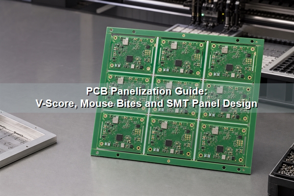
PCB panelization arranges multiple circuit boards within one manufacturing panel so fabrication, solder paste printing, placement, reflow, inspection and handling can process them as a stable unit. A useful panel is not simply the layout that fits the most boards. Its outline, rails, spacing, separation method, tooling features and component clearances must match the fabricator’s CAM rules, the assembly line and the final depaneling process.
What Is PCB Panelization?
PCB panelization converts one PCB design, or a controlled set of compatible designs, into a larger array that production equipment can transport and process. The finished panel normally includes the repeated board images, panel rails, separation features, global fiducials, tooling holes and identification marks. After assembly and testing, the individual boards are separated by V-scoring, routing, punching, sawing or laser cutting as appropriate.
A single PCB may be large and rigid enough to run without a delivery array, but small, narrow, irregular or thin boards often need added support. The phrase panelization construction is sometimes used for the complete arrangement of boards and temporary panel features. Practical PCB panelization guidelines must therefore define both the customer delivery panel and the fabricator-controlled production panel, which may include several delivery panels plus test coupons.
Why Is Panelizing PCB Important for Fabrication and SMT Assembly?
Panelizing PCB designs reduces repeated handling and gives conveyors, printers, placement machines and inspection systems a consistent rectangular workpiece. Several boards can pass through one stencil print, one placement program and one reflow cycle. Panel rails also protect edge components and create room for machine references that would not fit on a small finished board.
The benefit depends on the whole route. A dense array can improve laminate utilization but become too flexible under stencil pressure. A rigid array may process well yet waste material or impose excessive stress during separation. When the same supplier controls FR4 PCB fabrication and PCB assembly, CAM and SMT engineers can review the delivery panel against fabrication tolerances, stencil data, component placement and depaneling access before release.
Which PCB Panelization Methods Should You Choose?
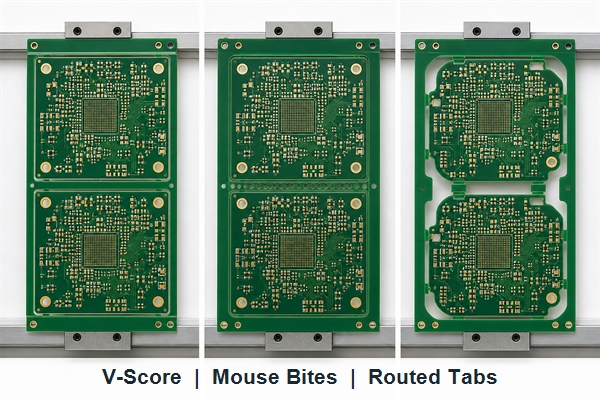
The separation method should be chosen before the array geometry is frozen. The main PCB panelization methods have different shape, spacing, stress and edge-finish limits.
- V-scoring: uses straight grooves from opposite sides of the panel. It is space-efficient for rectangular boards with continuous straight separation lines.
- Tab routing: routes most of the board outline while leaving solid tabs. It supports irregular contours and allows the tabs to be cut by a router.
- Mouse bites: add perforated holes to breakaway tabs for manual separation. A PCB panelization mouse bites pattern must match the fabricator’s drill and routing capabilities.
- Laser depaneling: provides a narrow, non-contact cut path for suitable materials and thicknesses, but it needs specialized equipment and process review.
- Punching or sawing: can suit stable high-volume geometries, although tooling cost or straight-line limits restrict their use.
The manufacturer should confirm channel width, residual web, tab placement and keepouts rather than relying on a universal online drawing. Material, finished thickness, copper distribution and component layout all change the result.
How Do V-Score and Tab Routing Compare?
The decision starts with board geometry and permitted separation stress. V-score favors straight outlines and high panel utilization. Tab routing accepts complex shapes and controlled tab locations but consumes area for the router path.
| Decision factor | V-score | Tab routing / mouse bites |
|---|---|---|
| Board outline | Straight, continuous separation lines | Curved or irregular outlines are possible |
| Board spacing | Boards may share a score line | Routing channel is required |
| Separation stress | Can flex a longer board edge | Localized at selected tabs |
| Finished edge | Straight scored edge | Tab witness may remain unless machine-routed flush |
| Component placement | Needs clearance from the score and flex zone | Needs clearance from tabs, router access and breakout force |
| Best fit | Rectangular, repeatable arrays | Irregular shapes and selective support points |
For more detail on breakout geometry, see the related guides to mouse bites versus V-groove and V-cut PCB depaneling. The production drawing should still use the dimensions approved for the current manufacturer and equipment.
What Panel Rails, Fiducials and Tooling Holes Are Required?
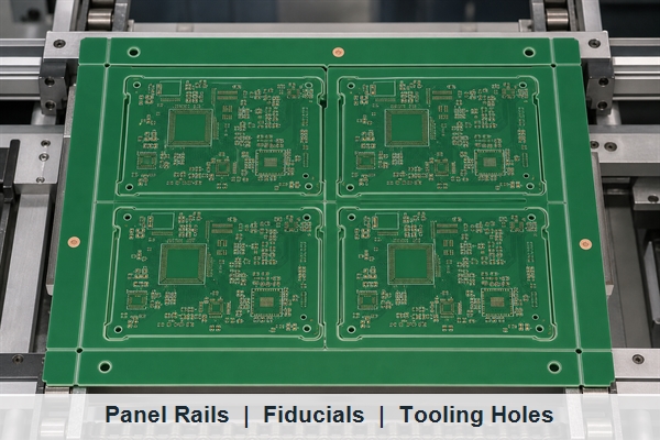
Panel rails create straight conveyor edges, increase stiffness and hold temporary production features. Their width follows the printer, conveyor, fixture and depaneling setup, not a fixed internet value. Rails may also carry global fiducials, tooling holes, barcodes, coupons and orientation marks.
Global fiducials establish panel translation and rotation for vision-guided equipment. An asymmetric arrangement reduces the chance of loading the panel in the wrong orientation. Tooling holes provide mechanical registration where a fixture or process requires it. Local board fiducials may still be needed near fine-pitch BGA, QFN or other placement-critical packages.
The panel data used to manufacture an SMT stencil must use the same board step-and-repeat, origin and orientation as the placement data. A stencil generated from a single-board paste layer cannot be assumed to match a later CAM-created array unless the duplication and datum transformation are controlled.
How Should PCB Panel Size, Spacing and Component Clearance Be Set?
A reliable PCB panel design starts with the usable machine envelope, then reserves rails, separation geometry and component keepouts before calculating the array count. Filling the entire fabrication sheet first can produce a panel that cannot be printed, transported or depanelized safely.
PCB panel size is constrained by every machine that must handle the panel, including fabrication equipment, stencil printers, pick-and-place systems, reflow conveyors, AOI, test fixtures and depaneling equipment. The smallest and largest usable dimensions, conveyor direction and rail requirements should be confirmed with the actual production route.
Board-to-board spacing follows the separation tool. V-score can place straight board edges together, while routing needs a channel wide enough for the selected cutter and positional tolerance. Laser separation may use a narrower path but requires material and thermal-process review. A PCB panelization calculator can estimate how many boards fit, but it cannot see every process restriction or guarantee the lowest finished-board cost.
Component clearance must include the body, solder joints, overhang, tool envelope and expected board flex. Ceramic capacitors, BGA corners, connectors and heavy parts close to a break line deserve particular attention because depaneling strain can damage a solder joint without leaving an obvious board crack. Copper, vias and controlled-impedance structures also need clearance from score grooves, routed channels and mouse-bite holes.
When Can Different PCBs Share One Panel?
Different PCB part numbers can share a panel only when their fabrication and assembly requirements are compatible. A mixed array generally needs the same material system, layer stack, finished thickness, copper weight, surface finish, solder mask process and production quantity ratio. If one design changes, the shared panel and its assembly data may also require revision.
A homogeneous panel containing one repeated design is easier to control, inspect and replenish. A heterogeneous panel can synchronize a product set and improve material utilization, but it may create unwanted inventory if the demand ratio changes. Rotated boards can improve nesting, yet their copper distribution and component orientation should be checked for reflow, wave soldering and inspection consistency.
Rigid-flex PCB and flex PCB panelization need additional attention to stiffeners, coverlay, bend regions, tooling support and final separation. Their temporary support strategy should be reviewed as part of the material and assembly process rather than copied from a rigid FR4 grid.
What Files Define the Panelization of PCB Arrays?
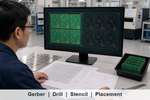
The panelization of PCB arrays should be defined by one controlled data package. At minimum, identify the finished panel outline, board origins, step-and-repeat, routing or scoring paths, tabs, fiducials, tooling holes, rails and critical dimensions. The fabrication data and the drawing must agree.
- Gerber or ODB++: copper, mask, legend, profile and panel-level production features.
- NC drill and rout files: tooling holes, mouse bites, slots and routed channels.
- PCB panelization drawing: overall dimensions, board arrangement, break features, datums and notes.
- Pick-and-place data: component coordinates transformed to the panel origin and repeated orientation.
- Paste and stencil data: the same array count and datum used by assembly.
- Assembly drawing: panel orientation, board references, special handling and depaneling restrictions.
Do not submit a customer-created panel Gerber together with a single-board NC drill or placement file unless the relationship is explicitly controlled. Mismatched repetition counts, origins and rotations are a common source of preventable CAM and assembly questions.
Which PCB Panelization Software and Tools Are Useful?
A PCB panelization tool is useful for layout exploration, but the correct choice depends on who owns the production data. PCB panelization software inside ECAD can preserve design links; CAM software can duplicate manufacturing layers, drill data and net information; a PCB panelization calculator is best treated as an early utilization estimate.
- PCB panelization Altium workflows: Embedded Board Array and Draftsman can create repeated arrays and fabrication drawings. Searches for Altium PCB panelization and Altium Designer PCB panelization normally refer to these functions.
- PCB panelization KiCad workflows: plugins or hierarchical layout methods can create arrays, but users should verify Gerber, drill, position and reference-designator output. The phrase KiCad PCB panelization describes the same task from the tool-first search direction.
- Fusion 360 PCB panelization: users should confirm whether the selected Electronics/EAGLE workflow exports every required manufacturing and assembly layer for the array.
- Free PCB panelization software: may be adequate for geometry trials, but output integrity, drill duplication, netlist consistency and revision control still require checking.
- Manufacturer CAM: usually offers the strongest alignment with actual material utilization, routing tools, panel borders and production equipment.
Software does not know every shop-specific limit. The released files should be checked in an independent CAM viewer and approved against the manufacturer’s panel drawing.
Should You Panelize the PCB or Let the Manufacturer Do It?
Let the manufacturer create the panel when the main goal is cost-efficient fabrication and the array has no product-specific mechanical constraints. Supply clean single-board data, state whether boards must arrive as a panel or separated, identify the assembly route and approve the returned panel drawing. This lets CAM use current working-panel sizes, routing tools and process margins.
Create and control the panel yourself when the assembly fixture, test nest, barcode position, mixed-design ratio, break sequence or customer equipment requires an exact delivery format. In that case, provide both the panel data and the original single-board source, then allow a DFM review. Ownership of the layout does not remove the manufacturer’s responsibility to flag incompatible geometry.
EBest Circuit (Best Technology) lists PCB dimensions up to 610 x 610 mm, subject to stack-up, material, panel utilization and engineering review. The published PCBA process includes 3D SPI, AOI, X-ray and functional testing. Those capabilities are useful only when the approved panel, stencil, placement data and inspection program share the same revision and datum.
How Does PCB Panelization Affect Cost and Yield?
Panelization changes cost through laminate utilization, machine handling, tooling, assembly cycle time, inspection and depaneling. Increasing the number of boards per panel can reduce handling per board, but a weak or warped array can increase paste defects, placement error or breakage. The lowest material scrap is not always the lowest total cost.
Compare layouts using finished good boards per panel, expected yield and all required operations. Include routing time, score setup, tab finishing, carrier or fixture needs, stencil size, test access and the labor or machine time required to separate boards. A mixed array can reduce material waste while increasing data control and inventory risk.
What Must Be Checked Before a PCB Panel Is Approved?
Approval should freeze the panel revision that fabrication, stencil, placement, inspection and test will use. Review the panel drawing and rendered CAM output together rather than approving a dimension table in isolation.
- Overall panel dimensions, thickness, quantity per panel and conveyor direction are stated.
- V-score, routing channels, tabs and mouse bites match the intended depaneling process.
- Rails, fiducials, tooling holes and orientation marks match SMT equipment and fixtures.
- Components, copper and vias have adequate clearance from every separation feature.
- Gerber/ODB++, NC drill, stencil, placement and assembly drawings use the same origin, rotation and revision.
- The panel remains sufficiently rigid through printing, placement, reflow, inspection and handling.
- Mixed designs share compatible stack-up, materials, finish and production ratio.
- First-panel separation verifies edge quality, strain-sensitive components and fixture access before volume release.
The related PCB panelization approval guide provides a focused release-control workflow. For the present project, keep the signed panel drawing with the manufacturing package so later revisions cannot silently change the array.
PCB Panelization FAQ
What Is Meant by PCB Panelization?
What is meant by PCB panelization is the temporary grouping of multiple boards into one production unit. The boards remain connected during fabrication or assembly and are separated after the required processes are complete.
Does Every Single PCB Need a Panel?
No. A sufficiently large, rigid and machine-compatible single PCB may run without a delivery array. Small, irregular, thin or edge-sensitive boards usually benefit more from rails and repeated panel processing.
Can a PCB Panelization Calculator Produce Final Manufacturing Data?
It can estimate board count and utilization, but final data still needs routing, score, rail, tooling, fixture and equipment review. Treat the result as a layout proposal rather than automatic production approval.
Can Flex PCB Panelization Use the Same Rules as Rigid FR4?
Not automatically. Flex PCB panelization may use stiffeners, temporary carriers, tooling strips or material-specific separation methods. Bend regions, coverlay and thin-material handling require process-specific review.
Can the PCB Manufacturer Panelize Single-Board Gerbers?
Yes, and this is often the simplest route when the delivery panel has no fixed fixture constraints. State the required panel delivery, assembly process and depaneling preference, then approve the manufacturer’s drawing before production.
Conclusion
Effective PCB panelization connects board geometry with fabrication, SMT handling, separation and data control. Choose the depaneling method first, define rails and machine references, keep every production file on one datum and approve the rendered panel before release. For a DFM review of single-board or controlled panel data, contact EBest Circuit (Best Technology) at sales@bestpcbs.com.