Harsh service conditions rarely cause one neat, isolated failure. An outdoor controller may keep out rain but collect condensation after a cold night. A vehicle-mounted board may work on the bench, then develop cracked solder joints beside a heavy connector. The first task in PCB Fabrication for Harsh Environments is to identify which stresses can reach the board and how they can interact.
Put the operating conditions into the design package: powered temperatures at the board and known hot spots, cold-start temperature, condensation or wet exposure, vibration and shock at the mounting points, likely contaminants and required service life. These values guide the laminate, stackup, spacing, surface finish, component support, coating and enclosure. Test levels should come from the product’s actual use and governing requirements; copying a temperature or vibration profile from an unrelated assembly can qualify the wrong design.
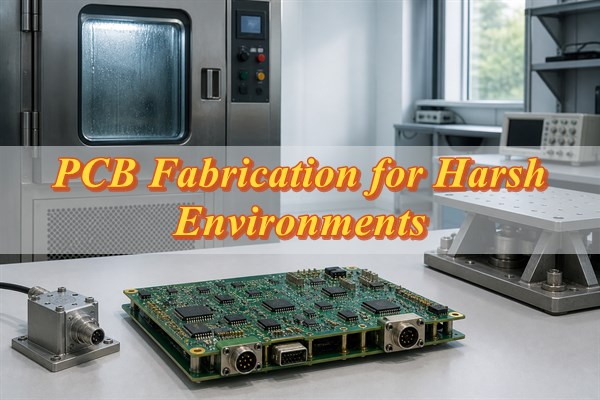
What Stresses Must PCB Fabrication for Harsh Environments Survive?
Start by following the board through its whole life, including shipping and storage—not just normal operation. A label such as “-40°C to 85°C” leaves out the details that often cause failures: ramp rate, dwell time, cycle count, self-heating and the temperature inside the enclosure. Those conditions decide how much strain reaches plated holes, solder joints and component terminations.
- Temperature: Record minimum and maximum board temperatures, ramp rates, dwell periods, cycling frequency and local hot spots. Separate ambient temperature from the temperature measured at the PCB and components.
- Moisture: Distinguish high humidity from condensation, splash, water immersion and pressure washing. Condensation can create a conductive surface film even when the average humidity appears acceptable.
- Mechanical loading: Specify sine vibration, random vibration, shock pulses, mounting orientation, connector insertion forces and cable loads. Heavy components and tall connectors can amplify strain.
- Corrosion and contamination: Identify salt, sulfur-bearing gases, fuels, oils, cleaning chemicals, conductive dust and process residues. Their combination with moisture and electrical bias can be more damaging than any one factor.
- Pressure and radiation: Record operating altitude, pressure change and outdoor ultraviolet exposure where relevant. Specialized ionizing-radiation environments require a separate component and material qualification program.
Put the results in one environmental requirements table. For every exposure, record the condition, duration, powered state and acceptance criteria. Designers can then trace each material choice, layout rule, coating note and qualification test back to a real service condition.
How Do PCB Requirements Change for Outdoor, Automotive, Mining and Marine Equipment?
“Harsh environment” covers very different problems. A board that survives vibration in a dry vehicle cabin may corrode quickly in a salt-laden enclosure. Potting that protects mining electronics from conductive dust may create an unacceptable thermal bottleneck in hot industrial equipment. The installation location matters more than the industry label.
| Application | Dominant risks | PCB and assembly priorities | Verification focus |
| Outdoor equipment | Condensation, rain ingress, ultraviolet exposure, daily thermal cycling and airborne pollution | Drainage and enclosure sealing, moisture-tolerant spacing, coating compatibility, corrosion-resistant hardware and controlled thermal expansion | Temperature-humidity exposure, ingress verification at the equipment level and powered functional checks |
| Automotive equipment | Wide temperature range, repeated thermal cycling, vibration, shock, fluids and connector loading | Rated components, robust interconnects, restrained heavy parts, appropriate laminate properties and strain-aware mounting | Vehicle-location-specific thermal, vibration, shock and electrical tests |
| Mining and underground equipment | High humidity, conductive dust, corrosive gases, impact, vibration and difficult maintenance access | Contamination barriers, cleanable construction, sealed interfaces, mechanical retention and documented inspection access | Humidity, dust or enclosure testing, vibration and post-exposure insulation checks |
| Marine equipment | Salt mist, saline condensation, galvanic corrosion, water ingress and persistent humidity | Compatible metals, corrosion-resistant finishes, complete edge coverage, sealed connectors and a coordinated coating/enclosure system | Salt or mixed-corrosion testing selected for the service condition, followed by electrical and visual inspection |
Use the table as a starting point, then narrow it to the actual installation. An engine compartment, sheltered control cabinet, exposed mast and submerged housing should not inherit the same test severity simply because each belongs to a familiar industry category.
How Do You Convert the Mission Profile Into PCB Fabrication Requirements?
Map each service stress to a design requirement, a production check and a verification method. A note such as “use high-reliability materials” does not identify a laminate property, acceptance limit or inspection record, so the fabricator cannot build or verify it consistently.
Step 1: Specify the operating state. Record whether the assembly is powered, unpowered or cycling during each exposure and identify safety-critical functions that must remain available.
Step 2: Identify the failure mechanism. Link temperature cycling to interconnect fatigue, humidity and bias to leakage or electrochemical migration, vibration to solder and connector fatigue, and corrosive agents to finish or metal attack.
Step 3: Select the design control. Assign a material property, stackup constraint, spacing rule, mechanical support, coating system, enclosure feature or process-cleanliness control.
Step 4: Write the production requirement. Put the approved material, tolerance, process note, inspection method and allowed substitution rule into controlled fabrication or assembly data.
Step 5: Set verification and acceptance criteria. Specify samples, preconditioning, exposure sequence, powered state, measurements and pass/fail limits before prototypes are built.
Service life and maintenance belong in the same discussion. A coated board that can be inspected and repaired is a different product from a permanently potted module, even if both pass the initial moisture test. Their heat flow, failure analysis and field-service options will never be the same.
Which Laminate Properties Matter in PCB Fabrication for Harsh Environments?
Choose the laminate for the expected failure mechanism, not for the largest Tg number on a datasheet. Tg marks a change in polymer behavior; it does not tell you, by itself, how long a powered assembly can run at a given temperature. Review the material data together with the finished stackup and the thermal cycles the board will see.
- Tg and modulus behavior: These influence dimensional stability and how the board responds as temperature crosses the transition region.
- Decomposition temperature and time to delamination: These help evaluate fabrication and assembly thermal robustness, but they do not replace an application operating-temperature rating.
- Z-axis coefficient of thermal expansion: Expansion through the board thickness strains plated through holes and stacked interconnects during temperature changes.
- Moisture absorption and insulation behavior: Moisture can change electrical performance and increase the risk of leakage or corrosion when contamination and bias are present.
- CAF resistance: Conductive anodic filament risk depends on material system, geometry, processing, contamination, humidity and bias. A material claim alone does not qualify the finished design.
- Copper adhesion and mechanical properties: These matter where flexing, heavy copper, thermal cycling or repeated shock can load conductor interfaces.
On the purchase drawing, name the laminate manufacturer and grade, prepreg construction, cured thickness and copper foil type. If substitutions are allowed, list the properties that must remain equivalent and the evidence needed for approval. “Same Tg” is too narrow to control a material change.
How Should Copper, Vias and Layout Withstand Heat and Vibration?
Copper and vias have to carry electrical and thermal loads without becoming fatigue sites. Heavier copper can reduce conductor temperature rise, but it also changes etching, resin flow, thermal balance and soldering behavior. Give the fabricator the complete stackup and load case instead of an isolated copper-weight request.
For plated holes, check the finished diameter, board thickness, aspect ratio, deposited copper, resin system and expected cycle count together. Blind and buried microvias deserve a stackup-specific qualification plan. Each added stacked interface is another place where expansion mismatch can concentrate strain.
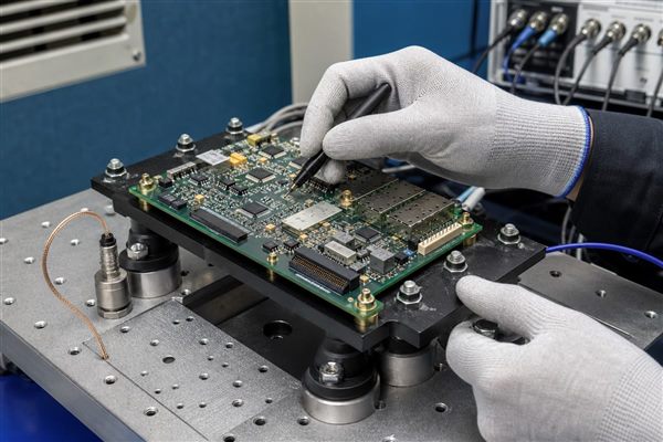
- Distribute heat: avoid concentrating major heat sources and expansion in one board region.
- Trace the heat path: use thermal vias and copper spreading only after checking where the heat can actually leave the assembly.
- Control board bending: place mounting points so flexure does not peak beneath large packages or connectors.
- Restrain heavy parts: add support and strain relief for transformers, large capacitors, relays, connectors and cable assemblies.
- Protect brittle parts: keep sensitive solder joints and ceramic components away from scored edges and highly loaded mounting points.
- Test the real structure: prototype with the intended enclosure, fasteners, cables and supports because fixture stiffness changes resonant behavior.
A continuity check after vibration can miss a joint that is cracked but still touching. Inspect fasteners, staking, connector retention, solder joints and permanent board deformation, and compare functional measurements from before and after the exposure.
How Do Pollution Degree, Creepage, Clearance and Altitude Affect the PCB?
Calculate clearance and creepage as separate insulation paths. Clearance is the shortest path through air, so its required value is driven by the voltage stress, field conditions and installation altitude. Creepage follows the insulating surface, so working voltage, material group, pollution degree and the expected surface condition become central inputs. A single generic spacing value can therefore be wrong for both paths.
Start with the product-specific safety standard. When it refers to IEC 60664-1, document the voltage inputs, material group, pollution degree and operating altitude before selecting distances from the applicable method. The standard’s current consolidated edition covers low-voltage insulation coordination, applies up to 2,000 m and provides guidance for higher-altitude use; a product standard may impose different or additional requirements.
Evaluate coating only after the uncoated spacing basis is clear. A coating or potting process does not automatically permit smaller distances; any reduction depends on what the governing standard recognizes and on controlled material, coverage and verification. Put the approved spacing values, coating keep-outs, test points, board edges and high-voltage zones in the fabrication and assembly data so the supplier can build and inspect the same insulation design.
Which PCB Surface Finishes Better Resist Corrosion and Exposure?
Select the surface finish for the interface it must create and the exposure it will actually see. The finish protects copper through storage and assembly and provides a soldering, contact or bonding surface. It cannot compensate for poor cleaning, an open enclosure or missing protection on field-exposed metal.
| Finish family | Useful characteristics | Harsh-environment questions |
| ENIG | Flat solderable surface and common availability | Confirm process control, nickel/gold integrity, storage conditions and whether exposed finished areas remain after assembly |
| ENEPIG | Supports several assembly and bonding interfaces when properly specified | Verify the full layer system and whether the added interface is needed for the actual assembly |
| Immersion silver | Flat surface with good solderability when correctly handled | Review packaging, storage and sulfur-bearing exposure; do not leave vulnerable areas unprotected in a corrosive environment |
| Immersion tin | Flat solderable finish | Control thickness, storage, handling and assembly timing under the applicable specification |
| OSP | Thin organic copper protection suited to controlled assembly processes | Assess handling, thermal excursions, shelf life and whether field-exposed copper protection is required |
| HASL | Established solderable finish with robust coverage for many conventional assemblies | Check planarity needs, thermal exposure and compatibility with fine-pitch or specialized interfaces |
Do not stop the metal review at the PCB. Connector plating, fasteners, shielding, enclosure alloys and conductive adhesives may all share the same moisture film. Two individually acceptable metals can still form a damaging galvanic couple when connected by an electrolyte.
How Should Components, Connectors and Heavy Parts Be Secured?
Solder joints should not be the only structure holding a heavy or tall component in place. Brackets, clamps, staking, cable strain relief, extra supports or local encapsulation can move the load into the chassis or board mounts. Check every added material against the operating temperature, coating process, rework plan and nearby plastics.
- Use qualified limits: set unsupported component mass and height from validated design rules, not a generic internet threshold.
- Preserve access: keep staking away from test points, mating surfaces, vents and inspection areas unless the drawing permits coverage.
- Unload connectors: transfer insertion, extraction and cable forces into the chassis or fasteners instead of flexing the PCB.
- Check expansion mismatch: pay particular attention to large leadless packages, ceramic components and rigidly bonded parts.
- Control hardware: specify torque, locking method, washer arrangement and inspection requirements for board mounts.
- Test the assembly: include the intended enclosure and harness because a bare-board fixture can hide system-level loads.
When Should You Use Conformal Coating, Potting or a Sealed Enclosure?
Choose the protection method by deciding where the barrier should sit. Conformal coating protects the board while preserving inspection and some repair access. Potting creates a more complete local barrier and adds mechanical support, but brings extra mass, thermal resistance and difficult rework. A sealed enclosure keeps contaminants away from the whole assembly. In practice, products often combine two of these measures in selected areas.
When comparing conformal coating vs potting, inspect the awkward places first: component leads, capillary gaps, connectors, board edges and mounting hardware. These are where an attractive flat-board coating sample can misrepresent production coverage. Model heat flow before adding resin around power components; the same material can spread heat toward a chassis or insulate the component, depending on conductivity, thickness and contact geometry.
IPC-CC-830C addresses conformal-coating material qualification and performance. A material qualification is useful, but it does not qualify your spray pattern, cure, thickness or coverage on a populated board. Those are production variables, and representative assemblies still need environmental testing.
How Should EMS Providers Control Assembly, Cleaning, Coating and Final Inspection?
The EMS process can either preserve the environmental design or quietly defeat it. Coating a contaminated assembly is a common example: residues remain under the film, moisture finds a path to them, and leakage or electrochemical migration begins where inspection is most difficult.
Step 1: Verify incoming materials. Confirm PCB identity, component moisture controls, coating and staking shelf life, storage conditions and lot traceability.
Step 2: Control soldering and rework. Qualify paste, flux, thermal profiles and manual processes as a combined residue and workmanship system.
Step 3: Clean where the risk assessment requires it. Select chemistry, time, temperature, agitation, rinse and drying controls that reach low-standoff areas without damaging materials.
Step 4: Validate cleanliness. Use methods appropriate to the failure risk. Bulk ionic testing, ion chromatography and surface insulation resistance answer different questions and should not be treated as interchangeable pass labels.
Step 5: Mask and coat consistently. Protect connectors, test points, thermal interfaces and other keep-out zones. Control material mixing, viscosity, application method, thickness and cure.
Step 6: Inspect the completed assembly. Check coverage, bubbles, pinholes, cracks, dewetting, contamination, staking, fasteners and masked areas with the specified lighting or fluorescence method.
Step 7: Run electrical tests. Perform the defined functional, insulation and safety tests after all protective materials have cured.
What Files Are Required for PCB Fabrication for Harsh Environments?
Put mandatory requirements, allowed substitutions and deliverable evidence in the controlled production package. If the stackup is in one email, the coating keep-outs in another and the test criteria in a meeting note, the supplier cannot quote or build against one reliable revision.
- Stackup: approved laminate system, copper foil, layer construction, finished thickness and controlled-impedance requirements.
- Interconnects: copper weights, finished hole sizes, plating requirements, via fill or cap instructions and allowed repair criteria.
- Board protection: surface finish, solder mask, marking materials and exposed-metal protection.
- Insulation: minimum creepage, clearance, high-voltage keep-outs, slots and coating boundaries.
- Assembly mechanics: component ratings, alternates policy, connector plating and support details.
- Special processes: cleaning, bake, masking, coating, staking, potting, cure and rework instructions.
- Inspection: test coupons, microsections, electrical test, AOI, X-ray and other required evidence.
- Qualification: environmental test plan, specimen configuration and pre/post-test measurements.
- Traceability: lot records, deviation approval, process-change notification and record-retention requirements.
What Qualification Evidence Should Procurement Request From PCB and EMS Suppliers?
Ask for evidence that identifies the design, lot or qualified process you are buying. Match each record to the purchase order, controlled drawing revision, material lot or assembly lot so the delivered evidence can be traced to the hardware.
- Material evidence: laminate and prepreg identity, approved substitutions, date or lot traceability and relevant supplier datasheets.
- Bare-board evidence: final stackup, electrical-test result, impedance data where required, microsection results and acceptance records for the specified interconnects.
- Assembly evidence: approved BOM and alternates, soldering profiles where contractually required, inspection results, rework history and cleanliness validation.
- Protection evidence: coating or potting material lot, application settings, cure record, measured thickness or coverage verification and defect disposition.
- Qualification evidence: test plan, specimen identity, calibration status, raw or summarized measurements, photographs and pre/post-test functional results.
- Change control: documented notification and approval before changing laminate, chemistry, coating, facility, critical process or component source where the contract requires it.
Which Tests Qualify PCB Fabrication for Harsh Environments?
A useful qualification test stresses the same mechanism that threatens the product in service. The IEC 60068 series provides widely used environmental methods, and IPC methods cover relevant board, coating and cleanliness properties. The mission profile and governing product standard still decide the method, severity, powered state and sequence.
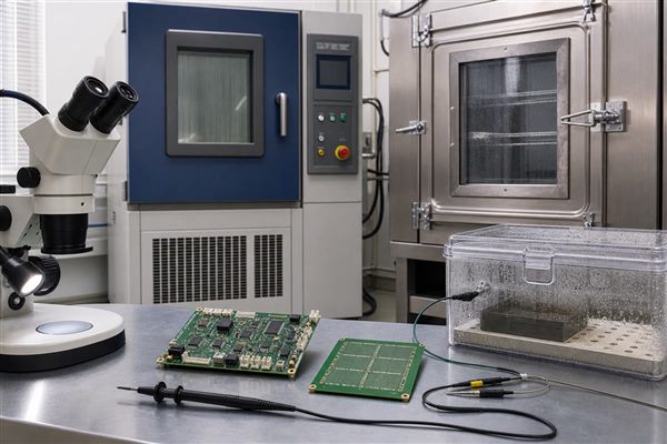
| Test family | Primary question | Evidence to retain |
| High and low temperature | Does the assembly function and remain within component, material and interface limits? | Board and component temperatures, operating state, functional data and visual inspection |
| Thermal cycling or thermal shock | Can interconnects, solder joints and material interfaces survive repeated expansion mismatch? | Profile, cycle count, continuity monitoring, resistance change, X-ray or microsection where justified |
| Damp heat or temperature-humidity-bias | Will moisture, contamination and electrical bias cause leakage, corrosion or migration? | Humidity and temperature record, bias conditions, insulation or SIR data and failure-site analysis |
| Vibration and mechanical shock | Do the board, fasteners, connectors and heavy components survive the system load? | Fixture and orientation, acceleration spectrum, resonance information, functional monitoring and post-test inspection |
| Salt mist or mixed-corrosion exposure | Are exposed metals, finishes, coating edges and enclosure interfaces resistant to the expected corrosive environment? | Solution or gas conditions, specimen orientation, exposure sequence, corrosion rating and electrical results |
| Electrical safety and function | Does the protected assembly maintain insulation, withstand voltage and required operation? | Test voltage or operating conditions, leakage or insulation values, functional limits and calibration records |
Sequence can change the result. Vibration may open a coating crack that only becomes electrically significant during the following humidity exposure. On the other hand, piling tests together without a failure-mechanism rationale can leave you unable to identify the initiating cause. Keep an untested control sample when it will help separate normal build variation from environmental damage.
How Should Harsh-Environment PCB Failures Be Diagnosed?
Begin failure analysis with the symptom, exposure history and physical evidence—not with the first damaged component. Replacing that component may restore operation while leaving the initiating cause, such as corrosion, cracked plating, contamination or mechanical strain, on the board.
Step 1: Preserve evidence. Record operating conditions, enclosure state, contamination, connector condition and failure timing before cleaning or disturbing the assembly.
Step 2: Localize the electrical symptom. Compare rails, insulation resistance, signal integrity, intermittent continuity and temperature behavior with a known-good unit.
Step 3: Inspect non-destructively. Use controlled visual inspection, microscopy, X-ray, ultraviolet coating inspection and thermal imaging as appropriate.
Step 4: Target destructive analysis. Cross-section suspect vias or solder joints, analyze residues or corrosion products, and examine interfaces only after the location has been narrowed.
Step 5: Reconstruct the mechanism. Decide whether the initiating condition was moisture, contamination, thermal fatigue, vibration, material incompatibility, coating defect, enclosure ingress or a combination.
Step 6: Verify corrective action. Update the design or process and repeat the stress that reproduced the failure, including post-test electrical and physical checks.
Useful clues include opens that appear only at certain temperatures, dendritic growth between biased conductors, corrosion products near residue, circumferential barrel cracks, solder fatigue beside heavy connectors and coating separation over a dirty or poorly cured surface. Each clue narrows the investigation; none should be called the root cause until inspection and analysis support it.
FAQs About PCB Fabrication for Harsh Environments
Q1: Can standard FR-4 be used in a harsh environment?
A1: Yes, in some applications. FR-4 is a family of materials, not one performance grade. Compare the selected grade’s thermal, expansion, moisture, electrical and CAF-related properties with the mission profile. Coating and enclosure protection may make it suitable for one installation, while another needs a different laminate or substrate.
Q2: Does a high Tg make a PCB suitable for continuous high-temperature operation?
A2: No. A high Tg does not by itself establish a PCB’s allowable continuous operating temperature. Review the laminate manufacturer’s long-term thermal data or applicable RTI, while treating Td and time-to-delamination results as short-duration thermal-robustness indicators rather than service-temperature ratings. Then check component and connector limits, plated-hole and solder-joint fatigue, coating limits, and measured board and component temperatures under power.
Q3: Can conformal coating make a PCB waterproof?
A3: No. Conformal coating is not a waterproof enclosure. Moisture can enter through coverage gaps, connectors, board edges, capillary paths or mechanical damage. Splash, immersion and pressure washing normally require equipment-level sealing and representative ingress testing.
Q4: Must a no-clean assembly be cleaned before coating?
A4: Decide from process validation, not from the “no-clean” label. Residue amount and chemistry, component standoff, humidity, electrical bias and coating adhesion all affect the result. Use a cleanliness method that can detect the failure risk you are trying to control.
Q5: Is potting always better than conformal coating for marine electronics?
A5: No. Potting trades serviceability and thermal freedom for a stronger local barrier. Marine reliability still depends on enclosure sealing, connectors, compatible metals, edge coverage and keeping saline moisture away from interfaces.
Q6: What is the main PCB risk in underground mining equipment?
A6: The combination of moisture and contamination is often the first concern. Conductive dust, corrosive gases, vibration and limited maintenance access can compound it. Document the actual atmosphere and safety requirements before choosing materials, spacing, enclosure and protection processes.
Q7: Are thermal shock and temperature cycling the same test?
A7: No. The transition rate and heat-transfer conditions are different. Select the method that reproduces the intended failure mechanism and meets the applicable standard; the two names are not interchangeable test specifications.
Q8: How is conformal coating thickness verified?
A8: Use a method matched to the coating and the location being controlled. Options include wet-film checks, cured witness coupons, mechanical or electronic gauges and microscopic cross-sections. One easy measurement on a flat area may say nothing about coverage around leads and board edges.
Q9: Does heavier copper solve every high-temperature PCB problem?
A9: No. Heavier copper solves only part of the thermal problem. Component losses, dielectric limits, via reliability, enclosure temperature, airflow and interface resistance remain in the heat path. Heavier copper also changes fabrication and soldering constraints.
Q10: How can procurement verify a supplier’s harsh-environment experience?
A10: Request evidence tied to the proposed construction. Useful records include material controls, final stackup, microsections, cleanliness and coating validation, environmental test documentation, traceability and change control. Each record should identify the applicable drawing, material lot or assembly lot.
Conclusion
Trace every important service stress to a drawing requirement, a production record and an acceptance test. If any link is missing from the harsh-environment PCB build package, the requirement is too vague for consistent production or a later failure investigation.
For a fabrication and assembly review, send the mission profile, stackup, Gerber or ODB++ data, BOM, assembly drawings and proposed qualification plan to sales@bestpcbs.com. The review is most useful when the operating environment and acceptance criteria arrive with the design files, not after the first prototype fails.
You may also like




Tags: conformal coating, Harsh Environment PCB, PCB Environmental Testing, pcb fabrication, Rugged PCB Design