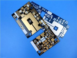
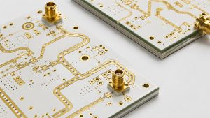
Choosing a high-frequency PCB manufacturer in USA requires more than comparing company names or the shortest advertised turnaround. The factory must be able to hold the approved RF laminate, dielectric thickness, copper profile, transmission-line geometry, via structure, impedance target, and verification plan as one controlled build.
A sound sourcing decision combines a verifiable US fabrication site, proven RF capability, lot-level quality evidence, relevant certifications, realistic lead time, and a quotation based on the same released design. The 15-manufacturer comparison connects those requirements to cost, USA-versus-overseas sourcing, and the information needed for a quote that can be compared line by line.
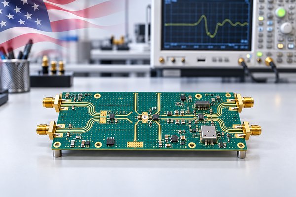
Top 15 High-Frequency PCB Manufacturers in the USA
The 15 companies have documented US operations and RF, microwave, low-loss, or related advanced PCB capabilities. Their addresses, manufacturing capabilities, lead times, and practical advantages identify which suppliers fit a project’s material system, board complexity, volume, and schedule. For a multi-site company, the quotation should name the plant that will fabricate the board.
| Manufacturer | Address | Manufacturing Capabilities | Lead Time | Practical Advantage |
|---|---|---|---|---|
| Sierra Circuits | 1108 W Evelyn Ave, Sunnyvale, CA 94086 | RF and microwave PCBs, PTFE and specialty laminates, controlled impedance, HDI and microvias, DFM, prototypes, and production support. | 3–5 days standard; 24-hour expedite for eligible builds. | Useful for engineering-intensive prototypes that need stackup, impedance, and manufacturability feedback before release. |
| AdvancedPCB | 21101 E 32nd Pkwy, Aurora, CO 80011; multi-site US network | Rogers, Taconic, PTFE, and other low-loss materials; mixed-material stackups; controlled impedance; HDI; via fill; and backdrilling. | Quick-turn available; final date follows material and plant review. | Multiple US facilities provide a broad prototype-to-production route, subject to site-specific capability confirmation. |
| Summit Interconnect | 223 N Crescent Way, Anaheim, CA 92801; multi-site US network | PTFE and low-loss materials, RF/digital hybrid stackups, controlled impedance, plated cavities and edges, controlled-depth milling, and via-stub control. | 5 days or less for eligible quick-turn builds. | Strong fit for complex defense, aerospace, and advanced-technology boards that need specialized processes and site-level qualifications. |
| Calumet Electronics | 25830 Depot St, Calumet, MI 49913 | RF and microwave boards, advanced and hybrid materials, HDI/HDBU, microvias, backdrilling, plated edges, dimensional control, and test support. | 3–5 weeks standard; 5–7 weeks with engineering work. | Domestic manufacturing with an emphasis on registration, process control, and traceable production for demanding programs. |
| TTM Technologies | 5823 Widewaters Pkwy, Suite 1, East Syracuse, NY 13057; global multi-site company | RF and microwave PCBs, hybrid dielectrics, material characterization, microvias, sequential lamination, cavities, and precision backdrilling. | Quoted after site, material, and process review. | Broad engineering and volume resources for programs that can match the design to a qualified TTM facility. |
| American Standard Circuits | 475 Industrial Dr, West Chicago, IL 60185 | RF/microwave, PTFE, metal-backed RF, hybrid constructions, precision machining, wire-bondable finishes, prototypes, and production. | 24 hours to 10 business days for eligible builds. | A focused option for RF boards that combine specialty laminates with metal-backed, machined, or bondable features. |
| Cirexx International | 791 Nuttman St, Santa Clara, CA 95054 | RF/microwave, hybrid FR-4/PTFE/Rogers stackups, controlled impedance and TDR, HDI and microvias, flex, and rigid-flex. | 1-day quick turn; 10–15 days standard by technology. | In-house US design, fabrication, and assembly coordination can reduce handoffs on prototype and complex interconnect work. |
| Royal Circuit Solutions | 21 Hamilton Ct, Hollister, CA 95023 | Rigid RF and high-speed boards, low-loss laminate support, controlled impedance, heavy copper, quick-turn prototypes, and production services. | Quoted after laminate allocation and stackup approval. | Responsive prototype service for teams that need a US build and a path from early revisions to repeat orders. |
| PNC Inc. | 115 E Centre St, Nutley, NJ 07110 | RF and microwave boards, Rogers and Taconic materials, hybrid stackups, controlled impedance, blind/buried vias, microvias, ENIG, and ENEPIG. | From 24 hours; RF/hybrid timing follows engineering review. | Design, bare-board fabrication, assembly, and test coordination are available through one US operation. |
| Custom Circuit Boards | 17650 N 25th Ave, Suite 2, Phoenix, AZ 85023 | Rogers, Teflon, Arlon, and Nelco materials; Rogers/FR-4 hybrids; multilayers; controlled impedance; blind/buried vias; and multiple finishes. | 24-hour, 2-, 3-, 5-, or 10-day prototype options. | Flexible prototype schedules for low-loss and hybrid constructions when the required material is available. |
| Compunetics | 700 Seco Rd, Monroeville, PA 15146 | RF, microwave, and millimeter-wave boards; PTFE and low-loss materials; mixed dielectrics; complex vias; cavities; edge plating; and metal-core constructions. | About 5 days quick turn; about 4 weeks standard. | US manufacturing with specialized RF structures and vertically coordinated electronics capabilities. |
| Accurate Circuit Engineering | 3019 S Kilson Dr, Santa Ana, CA 92707 | RF, antenna, and microwave PCBs; PTFE/FR-4 hybrids; controlled impedance; RF trenching; Rogers and Taconic materials; cavities; and TDR. | 24 hours to 20 days, depending on scope. | A specialized US source for prototype and low-volume RF work with unusual machining or hybrid-material needs. |
| Sanmina | 2945 Airway Ave, Costa Mesa, CA 92626; multi-site global company | Advanced rigid and rigid-flex PCBs, HDI, sequential lamination, hybrid materials, Rogers and Taconic low-loss systems, wire-bondable gold, and solid copper via fill. | Quoted after the fabrication site and scope are confirmed. | Suitable for complex programs that need advanced PCB fabrication integrated with broader product-manufacturing services. |
| Saturn Electronics Corporation | 28450 Northline Rd, Romulus, MI 48174 | RF and microwave boards, PTFE processing, metal-core thermal management, blind/buried vias, and via-in-pad structures. | Quoted after material and delivery review. | US fabrication for teams combining RF features with thermal-management or advanced-via requirements. |
| Imagineering | 2425 Touhy Ave, Elk Grove Village, IL 60007; US prototype/assembly operation | Rogers and PTFE prototypes, controlled impedance, HDI and microvias, multilayer fabrication, assembly, and production sourcing. | From 24 hours; small-volume builds around 5–6 days. | Fast prototype coordination, but buyers requiring domestic production should verify the factory for each production order. |
What Should You Consider When Choosing a High-Frequency PCB Manufacturer in the USA?
The right manufacturer is the specific factory that can repeat the complete RF construction at the required volume and prove it with order-level records. Site identity, material control, engineering response, verification, production transfer, and commercial scope determine whether that capability is credible.
- Actual manufacturing site: Ask which legal entity and street address will laminate, drill, plate, image, etch, finish, inspect, and electrically test the board. A US sales office, headquarters, or assembly line does not by itself prove US bare-board fabrication.
- Complete-build capability: Give the supplier the layer count, laminate system, copper, controlled geometry, via structure, finish, tolerances, and test plan together. Separate maximum values do not prove that the factory can combine every requirement in one build.
- Material and substitution control: Confirm the exact laminate grade, thickness, copper foil, bondply, stock status, approved alternates, and written approval process for changes. An unapproved material substitution can change impedance, loss, dimensional behavior, and qualification status.
- Engineering response: A useful DFM response identifies conflicts, proposes measurable alternatives, and returns the finished stackup and modeled geometry for approval. A simple “files look good” response leaves the important RF assumptions unresolved.
- Verification evidence: Match coupons, TDR, microsections, dimensional measurements, material certificates, electrical test, and RF measurements to the risks in the design. Ask who performs each test and what data will accompany the lot.
- Prototype-to-production control: Determine whether production will use the same site, materials, tooling logic, coupons, and test methods. If the route changes, require a documented transfer and a new approval build.
- Commercial transparency: Compare material, tooling, test, documentation, freight, duties, assembly, and nonrecurring charges under the same assumptions. A low unit price is not a saving if it excludes a required material or acceptance test.
Select only suppliers that return a named factory, an approved stackup, a test plan, a written exception list, and schedule dependencies. These five outputs make technical capability and commercial risk comparable before purchase.
What Manufacturing Capabilities Do High-Frequency PCB Manufacturers in the USA Offer?
Required manufacturing capability is determined by the electrical and physical construction: operating band, loss budget, power, layer count, via transitions, finish, and assembly interface. US suppliers differ most in how they combine low-loss materials, controlled impedance, hybrid lamination, advanced vias, precision machining, and RF-sensitive surface control.
- RF and microwave materials: Common options include hydrocarbon-ceramic laminates, PTFE systems, low-loss epoxy materials, bondplies, and mixed-material constructions. The factory should state the design Dk, test method, frequency, dielectric tolerance, copper profile, and thickness used in its impedance model.
- Controlled transmission lines: Manufacturers may support microstrip, stripline, grounded coplanar waveguide, differential structures, antenna features, and controlled connector launches. The returned model should show finished trace width, gap, copper thickness, dielectric thickness, and target tolerance.
- Hybrid and multilayer lamination: RF laminate combined with FR-4 can reduce cost or add mechanical support, but the factory must control bonding, resin flow, copper balance, registration, z-axis movement, drilling, and desmear for the chosen materials.
- Advanced vias and depth control: Blind/buried vias, microvias, via-in-pad, filled vias, backdrilling, controlled-depth milling, cavities, and plated edges can reduce stubs or support compact RF packaging. Ask for achievable tolerances on the actual board thickness and material set.
- RF-sensitive surface control: Copper roughness, final finish, solder mask over or beside RF traces, cleanliness, flatness, and wire-bondable surfaces may affect loss, assembly, bonding, or mechanical fit. Define the acceptance method instead of relying on a finish name alone.
- Prototype, production, and assembly: Some suppliers provide only bare boards; others coordinate components, assembly, RF connectors, shielding, programming, and functional test. If assembly is included, separate bare-board acceptance from assembled RF performance so a failure can be traced correctly.
Approve the complete process window before release: laminate and foil, finished stackup, modeled transmission-line geometry, via and machining limits, surface finish, and the prototype-to-production route. A material name alone does not show that one factory can hold every RF-critical feature in the same build.
How Can You Evaluate the Quality of High-Frequency PCBs From USA Manufacturers?
Quality is demonstrated when every RF-critical feature has an agreed measurement and a lot-specific record. The evaluation should trace the approved stackup through representative coupons, physical inspection, electrical testing, material identity, and repeat-lot trends.
- Approve the finished stackup: Compare the manufacturer’s proposed dielectric thicknesses, copper build, design Dk, copper profile, trace geometry, and impedance model with the released design. The observable result is a signed or revision-controlled stackup before tooling.
- Define representative coupons: Specify the structures, target, tolerance, panel location, test method, and reporting format for impedance coupons. A valid coupon should use the same relevant material, copper, lamination, and process as the board feature it represents.
- Inspect physical construction: Use microsections, plating-thickness measurements, dielectric and finished-thickness records, backdrill depth, critical dimensions, registration data, and material certificates where they address actual risk. Sampling and acceptance limits should be agreed before the order.
- Separate electrical tests: Bare-board continuity and isolation detect opens and shorts. TDR evaluates impedance and discontinuities. Insertion loss, return loss, phase, coupling, resonant behavior, and assembled function require different fixtures, reference planes, frequency ranges, and acceptance limits.
- Review lot traceability: Check the laminate lot, date code, traveler, inspection results, equipment or test identity where required, certificate of conformance, and documented deviations. The records should point to the same site and revision named on the purchase order.
- Compare repeat lots: Track impedance, critical dimensions, plating, yield, defects, and RF data across lots. A trend toward a limit is more actionable than a single pass/fail value because it can trigger correction before field performance changes.
A complete quality record lets engineering compare the delivered board with the approved model and isolate whether a deviation came from material, fabrication, assembly, the test fixture, or the circuit design. If the records cannot support that diagnosis, the acceptance plan is incomplete.
Which Certifications Matter When Choosing a High-Frequency PCB Manufacturer in the USA?
Certifications matter only when their site, scope, and validity match the factory and end market named on the purchase order. Use ISO 9001 for general quality-system screening, then add aerospace, medical, automotive, defense, UL, or customer approvals only when the program requires them.
- Match the address and legal entity: Compare the certificate name, site, scope, issue date, expiration date, and standard revision with the factory on the quotation. A corporate certificate may not include every facility.
- Separate quality systems from product acceptance: A management-system certificate shows that a process framework has been audited; it does not prove that one RF lot met impedance, loss, material, dimensional, or reliability requirements.
- Name the performance specification: IPC-6018D addresses qualification and performance requirements for microwave printed boards. State the applicable class, board type, addendum, deviations, coupons, and acceptance details in the procurement documents.
- Check program-specific obligations: Aerospace, defense, medical, automotive, telecom, and controlled-data programs may require different approvals, record retention, traceability, source restrictions, or change notification. Translate those needs into purchase-order clauses.
- Verify continuing validity: Review certificate status before supplier approval and again when the site, scope, ownership, or process route changes. Require notice when a relevant approval is suspended, expires, or no longer covers the product.
Treat certification as an entry requirement and lot evidence as acceptance proof. Approve the supplier only when the certificate covers the named site and the purchase order separately defines the board’s measurable quality requirements.
How Long Does High-Frequency PCB Manufacturing Usually Take in the USA?
US prototype lead time can range from one to five working days for a material-ready, straightforward board; hybrid laminates, HDI, special finishes, RF testing, or customer documentation can extend the build to several weeks. A credible schedule begins after material allocation and engineering release and ends at the agreed delivery point.
- Engineering closure: Incomplete stackup, impedance, material, finish, panel, test, or documentation requirements delay release. Ask the supplier to list every open item and identify the date on which the manufacturing clock starts.
- Material readiness: “Supported material” is not the same as material reserved for the order. Confirm grade, thickness, copper, minimum purchase, stock location, shelf life, and procurement time before accepting an expedited promise.
- Process route: Extra lamination cycles, laser drilling, via fill, backdrill, cavities, edge plating, sequential inspection, outsourced finishes, or RF testing add dependent operations. The schedule should identify the critical path and any outside service.
- Inspection and documentation: Coupons, microsections, dimensional reports, first-article inspection, source inspection, RF data, and customer record review need planned capacity. A board can be physically complete while the required acceptance package is not.
- Prototype-to-production transition: Production may use a different panel, material lot, tooling set, capacity window, or factory. Ask what transfers unchanged and which features require another approval build.
- Shipping endpoint: Distinguish fabrication complete, ex-works ship date, domestic delivery, and arrival at your assembly site. The comparison should include weekends, freight method, customs when applicable, and receiving inspection.
Accept a lead time only when it includes engineering release, material allocation, fabrication, inspection, shipment, and delivery milestones. This exposes the step responsible for delay and prevents a fast factory-complete date from being mistaken for the customer’s arrival date.
How Much Does High-Frequency PCB Manufacturing Cost in the USA?
High-frequency PCB cost is built from the approved construction, not a generic price per board. Laminate usage, layer count, RF geometry, special processes, yield risk, testing, quantity, documentation, and delivery scope determine whether two quotations describe the same product.
- Laminate and panel utilization: Material grade, thickness, copper foil, bondply, panel size, nesting efficiency, minimum purchase quantity, scrap, and shelf life determine more than the raw price per sheet.
- Construction complexity: Hybrid dielectrics, high layer count, multiple lamination cycles, thin cores, tight dielectric control, copper balance, and difficult registration increase process steps and can reduce yield.
- Geometry and special features: Fine RF gaps, filled microvias, backdrilling, cavities, plated edges, controlled-depth routing, metal backing, selective solder mask, and bondable finishes add tooling, processing, or inspection.
- Testing and records: TDR coupons, microsections, critical-dimension reports, RF test vehicles, third-party testing, first-article inspection, lot traceability, and customer-specific documentation should appear as included scope or separate charges.
- Order profile: Prototype setup, production quantity, recurring lot size, forecast stability, expedite priority, change frequency, assembly scope, and component sourcing affect unit and nonrecurring costs differently.
- Total landed cost: Add engineering time, freight, insurance, duties, inventory, schedule risk, requalification, corrective action, and communication overhead. A higher fabrication quote can be the lower-cost choice when it prevents a redesign or delayed system test.
A valid price comparison uses the same revision, material, tolerances, tests, documentation, quantity, and delivery terms. Recalculate any quote that substitutes a material, relaxes a limit, omits evidence, or changes the factory before choosing the lowest total.
USA vs Overseas High-Frequency PCB Manufacturers: What Is the Difference?
Compare USA and overseas factories on lead time, total cost, quality control, engineering support, production-location requirements, and capacity. Both routes should be judged against the same released stackup, acceptance evidence, quantity, and delivery endpoint.
| Decision Factor | USA High-Frequency PCB Manufacturers | Overseas High-Frequency PCB Manufacturers |
|---|---|---|
| Lead Time | Shorter domestic transit and same-time-zone engineering can speed prototypes and revisions. | Longer freight and customs time; production can scale efficiently after design release. |
| Cost | Unit prices are often higher, but freight, duties, and communication costs are lower. | Unit prices can be lower at volume; include freight, duties, inventory, and rework. |
| Quality Control | Easier site access and first-article review; verify process data and lot records. | Quality can be equivalent when controls, test data, and traceability are qualified. |
| Engineering Support | Same-time-zone access can shorten DFM, stackup, and deviation decisions. | Requires disciplined revision control, response times, and written technical records. |
| Production Location | Fits programs requiring domestic fabrication or controlled US data access. | Use when offshore production and data transfer are permitted and disclosed. |
| Capacity and Supply | Useful for low-volume, high-mix, or regulated work; capacity may be limited. | Often offers more volume flexibility; control materials, transfers, and requalification. |
What Information Do You Need to Provide for a High-Frequency PCB Quote?
A quotation from a high-frequency PCB manufacturer in USA is comparable only when every supplier receives the same design revision, stackup, material, electrical limits, inspection plan, quality requirements, quantities, and delivery terms. The RFQ should also require each factory to return its assumptions, exceptions, and proposed process route.
- Release package: Provide Gerber, ODB++, or IPC-2581 data as applicable; drill files; fabrication drawing; netlist; revision; units; quantities; panel preference; and document precedence. Require the supplier to confirm one quoted revision.
- Electrical requirements: State the operating band, impedance structures and tolerances, loss or phase limits where applicable, power concerns, controlled RF features, and the acceptance method for each requirement.
- Material definition: Name the laminate, bondply or prepreg, dielectric thickness, copper foil and profile, approved alternates, design Dk or model assumptions, finish, solder mask, and substitution-approval rule.
- Physical construction: Include the proposed stackup, finished copper, critical transmission-line dimensions, reference planes, via structures, backdrill, cavities, edge features, connector launches, controlled dimensions, and tolerances.
- Inspection and test: Define coupons, TDR, microsections, electrical test, critical dimensions, RF test vehicles or data, sampling, limits, report format, and treatment of a nonconforming result.
- Quality and traceability: Specify the applicable performance document, certification or customer approval, material and lot traceability, certificate of conformance, record retention, first-article needs, change notice, and approved site.
- Commercial scope: State prototype and production quantities, forecast, target delivery date and location, Incoterm, packaging, assembly and component scope, documentation package, freight assumptions, and quote validity.
- Required response: Ask for the named factory, material status, finished stackup, modeled geometry, process route, test plan, lead-time start and endpoint, tooling charges, unit prices, exclusions, and a line-by-line exception list.
A complete RFQ should return a named factory, material status, finished stackup, modeled geometry, test plan, schedule, price breakdown, and exception list. Resolve any missing output before technical or commercial approval.
FAQs About High-Frequency PCB Manufacturers in the USA
These five questions resolve common qualification gaps: RF versus high-speed design, FR-4 limits, proof of US fabrication, the scope of TDR, and prototype-to-production transfer.
Q1: Is a high-frequency PCB the same as a high-speed PCB?
A1: They overlap but emphasize different risks. High-frequency boards focus on RF or microwave behavior such as loss, impedance, radiation, coupling, and phase. High-speed digital boards focus on edge rate, timing, reflections, crosstalk, and power integrity. A mixed-signal board may require both disciplines, so the RFQ should name the actual structures and acceptance criteria.
Q2: Can standard FR-4 be used for a high-frequency PCB?
A2: Yes, when route length, frequency, loss budget, impedance tolerance, temperature, and unit-to-unit consistency leave enough margin. Model the real interconnect and compare predicted and measured performance. Use a lower-loss or more stable laminate when FR-4 attenuation or variation consumes the available margin.
Q3: Does a US address prove that the PCB is manufactured in the USA?
A3: No. The address may belong to a headquarters, sales office, engineering group, warehouse, or assembly site. Require the quotation and purchase order to identify the facility that performs bare-board fabrication and disclose any subcontracted or offshore operations.
Q4: Is a TDR report enough to qualify an RF PCB manufacturer?
A4: No. TDR can evaluate characteristic impedance and discontinuities under the agreed method, but it does not prove insertion loss, return loss, phase, material identity, plating reliability, or assembled RF function. Pair it with the physical, material, dimensional, and RF evidence required by the design.
Q5: Should the same factory build prototypes and production boards?
A5: Using the same factory can reduce transfer variables, but it is not mandatory. If production moves, freeze the material, stackup, artwork compensation, tooling assumptions, coupons, test methods, limits, and approved deviations, then requalify the transferred build before volume release.
Choosing a high-frequency PCB manufacturer in the USA requires one factory to match the RF material system, complete process route, quality evidence, certifications, lead time, cost, and production controls defined by the released design. The manufacturer table and USA-versus-overseas comparison narrow the field, while a complete RFQ confirms the stackup, tests, exceptions, schedule, and price under one revision.
If you need an overseas manufacturer that can produce high-frequency PCBs, contact us at sales@bestpcbs.com.