PCB manufacturing PCB manufacturing
Home > Blog

PCB Traceability

QR Code Marking on Copper: How to Make Codes That Scan Reliably
Monday, September 14th, 2026

QR code marking on copper works when a reader can distinguish the code’s small squares from the surrounding surface. The challenge is keeping that contrast through finishing, cleaning, and assembly. On a PCB, the marking process must also preserve the copper needed for the circuit.

A useful code starts with three decisions: what it must identify, where it will be placed, and when it must be scanned. This guide explains how those choices affect the marking method, code size, readability, and the production records a PCB or PCBA buyer can retrieve.
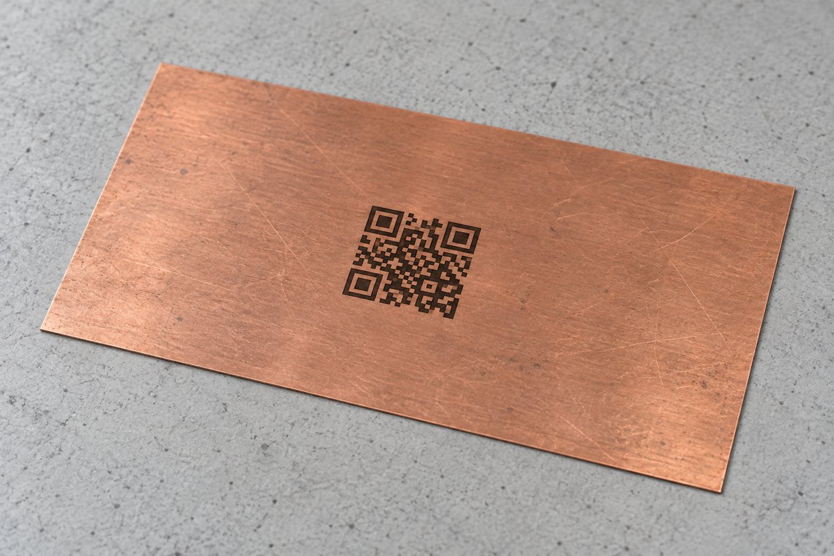
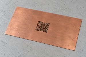
QR code marking on copper
AI illustration of a QR-style marking on a thin copper sheet.

What Is QR Code Marking on Copper?

QR code marking on copper creates a machine-readable pattern on a copper surface. Direct laser marking changes the surface’s appearance or texture; engraving removes material to form the pattern. A PCB can also carry a QR pattern formed in its copper artwork.

Each small square in a QR code is called a module. The reader must distinguish the two module states, recognize the corner patterns, and see a clear border around the symbol. That border is the quiet zone. On reflective copper, the contrast seen by the reader can change when the lighting or viewing angle changes.

The code’s purpose determines its data. A part number identifies a product type. A batch code identifies a production group. A unique serial number identifies an individual board or part. For traceability, that identifier can retrieve manufacturing records without storing all those records inside the code.

Which Methods Work for QR Code Marking on Copper?

Choose the method according to the surface being marked and whether the code must change from unit to unit. Several approaches can create a copper-related pattern, but they do not perform the same operation.

MethodSuitable starting pointImportant limitation
Direct laser markingA variable identifier on a copper surfaceContrast must be achieved within the part’s allowable surface change
Mechanical engravingA robust copper part that can tolerate material removalNot a default method for thin PCB copper foil
Patterned PCB copperA fixed identifier included in board artworkRepeated artwork repeats the identifier; it does not automatically serialize boards
Selective solder mask removalA pattern created by exposing copper beneath the maskThe process acts on the coating and must protect the underlying board

A fixed code and an individual serial number solve different problems. If every board only needs to identify the product model, a repeated artwork code may be sufficient. If each board needs its own test history, the production process must assign and apply a distinct identifier.

Also distinguish direct copper marking from exposing copper through solder mask. They may look similar in a photograph, but their process settings and failure modes differ.

Which Laser Works Best for Marking QR Codes on Copper?

A pulsed fiber laser is one established option for direct copper marking. Green and UV marking systems are additional candidates where the material response or fine-feature requirements call for a different wavelength. The best choice is the one that produces readable modules while staying within the part’s allowable surface change.

Pulsed infrared fiber lasers: Suitable settings can produce contrast on copper, but reflective copper requires careful control of the interaction. Pulse duration, focus, scan speed, and repeated passes affect the result. Raising average power alone does not resolve those variables.

Green and UV marking lasers: These offer different interactions with the material and can be evaluated for non-ferrous metals and fine marking tasks. A shorter wavelength does not automatically make a process safe for PCB foil. The actual spot size, pulse characteristics, and material stack still matter.

For a PCB, first distinguish direct copper marking from removing solder mask. The first changes the metal; the second should remove the intended coating while protecting the copper below. A successful demonstration on a thick copper part does not qualify either process for a finished board.

Compare samples at the intended code size and production speed. Reject a process that gives strong contrast but damages functional copper, or preserves the board but produces inconsistent scans. This gives the equipment choice a measurable target: readable codes on acceptable parts.

Why Won’t a QR Code on Copper Scan?

The most useful first question is whether the failure changes when you move the light or the reader. If it does, investigate reflections before changing the marking depth. If it does not, inspect the code geometry and reader setup.

SymptomWhat it suggestsWhat to check first
Reads only when tiltedAngle-dependent contrast or glareLighting arrangement and reader orientation
Small squares merge or vanishInadequate feature definitionModule edges, focus, and marking resolution
Reader cannot locate the symbolObstructed border or damaged corner patternsQuiet zone and the three finder patterns
Reads before processing but fails afterwardSurface change or contaminationThe operation between the last successful scan and the failure

Confirm that QR decoding is enabled on the reader. Check its working distance and field of view: a code can be sharply marked yet occupy too few image pixels to decode reliably.

Increasing laser power is not a general fix. It may change the surface or spread feature edges without solving glare. Likewise, QR error correction can tolerate some damage, but it cannot compensate for every loss of contrast or missing feature.

How Small Can a QR Code on Copper Be?

Calculate the required area from the encoded data and module size, including the quiet zone. Do not choose a marking area from the visible pattern alone.

A standard QR code requires a quiet zone four modules wide on each side:

Overall side length = (modules per side + 8) × module width

For a Version 1 code with 21 modules per side, an illustrative module width of 0.20 mm gives:

(21 + 8) × 0.20 mm = 5.8 mm per side, including the quiet zone.

This calculation defines the reserved area. It does not establish 0.20 mm as a suitable module size for every copper marking process or reader.

Consider a hypothetical board identifier, B260914001. A code containing that short identifier can retrieve a larger production record from a database. Encoding the full record instead may require more modules and therefore more space at the same module width. Confirm the actual data capacity and error correction setting before finalizing the layout.

If space is limited, shorten unnecessary data before shrinking the modules. Then confirm that the marking process can reproduce the resulting pattern and the intended reader can resolve it.

Should You Mark Copper Before or After Surface Finishing?

Marking before finishing exposes the pattern to later surface changes. Marking afterward gives you the final surface to work with, but may disturb the finish itself. Choose the sequence around both the finish’s function and the first required scan point.

Before finishing: Plating or coating can cover the marked surface or change how it reflects light. A contrast pattern that reads clearly on bare copper may look different afterward. If the mark relies on a particular surface color or texture, evaluate it after the complete finishing sequence.

After finishing: The code can be optimized for the surface the reader will actually see. However, engraving or removing that finish may expose underlying material or change a functional area. A code should not compromise a surface needed for protection, soldering, or electrical contact.

For example, a code required only during final inspection may be applied later than one needed to track the board through earlier production steps. If early processing would obscure the permanent mark, an earlier identifier must remain linked to the final board identifier.

For a PCB order, specify the finish, marking location, and when scanning must begin. A sample that scans before finishing answers a different question from a sample that scans after finishing and assembly.

When Can PCB Laser Marking Damage the Copper Layer?

PCB laser marking can cause damage when it removes or alters copper that the circuit needs. Excessive energy or repeated passes may thin a conductor, change a pad surface, or affect nearby mask and laminate.

A readable code is not proof that the board remains electrically acceptable. A deep mark may improve one aspect of contrast while reducing the copper cross-section. On a functional pad, surface changes may also interfere with its intended use.

Separate the permitted marking area from functional pads and traces during layout and manufacturing review. Do not assume that a visually empty copper area is electrically unimportant: a copper pour may be serving as a plane or current path.

When the process is intended to remove solder mask, review whether it stops at the intended layer. When it is intended to modify copper, define what surface change the design can tolerate. Relevant inspection or electrical checks should follow that mechanism, rather than treating every laser mark as the same risk.

Should You Place a QR Code on PCB Copper or Solder Mask?

Choose a location that remains accessible at the actual scan points. The board’s assembled condition can matter more than how convenient the location looks in the bare-board drawing.

Consider a solder mask area when it provides useful contrast and separates the marking operation from exposed functional copper. Its suitability still depends on mask color, thickness, and the marking process.

Consider a copper area when the identification requirement calls for it and the design provides a suitable region. Include the final finish and reflected light in the readability assessment.

Check for components, shields, connectors, and later coatings that could cover or obscure the symbol.

A panel-rail code can identify a panel during fabrication, but the rail is later removed. If individual boards need traceability afterward, map them to their own identifiers before that link disappears. Keeping a code visible and keeping its history connected are both part of placement planning.
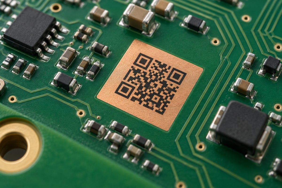
QR code marking on copper
AI illustration of a copper marking area on a PCB.

How Do You Verify a QR Code on Copper After Processing?

Check readability, decoded data, and the marked product separately. Each answers a different question.

Check the physical symbol. Inspect module edges, corner patterns, the quiet zone, and visible surface damage. Read the code with the intended reader at the working distance and lighting used in production. Include relevant finishing, cleaning, assembly, and coating steps in the evaluation.

Check the quality requirement. A successful phone scan demonstrates that one device decoded the symbol under those conditions. It does not establish a specified quality grade. Where grading is required, agree on the applicable verification method and lighting. ISO/IEC 15415 addresses two-dimensional symbol quality, while ISO/IEC 29158 addresses direct part marking quality. Select the applicable method and lighting for the actual marking application; do not assign a grade from a casual scan.

Check the identity and product. In the hypothetical example, B260914001 should retrieve the intended board’s record. A second board accidentally carrying that same identifier might scan perfectly while undermining individual traceability. Check for duplicate or incorrect values, and complete the physical or electrical checks required by the marking process.
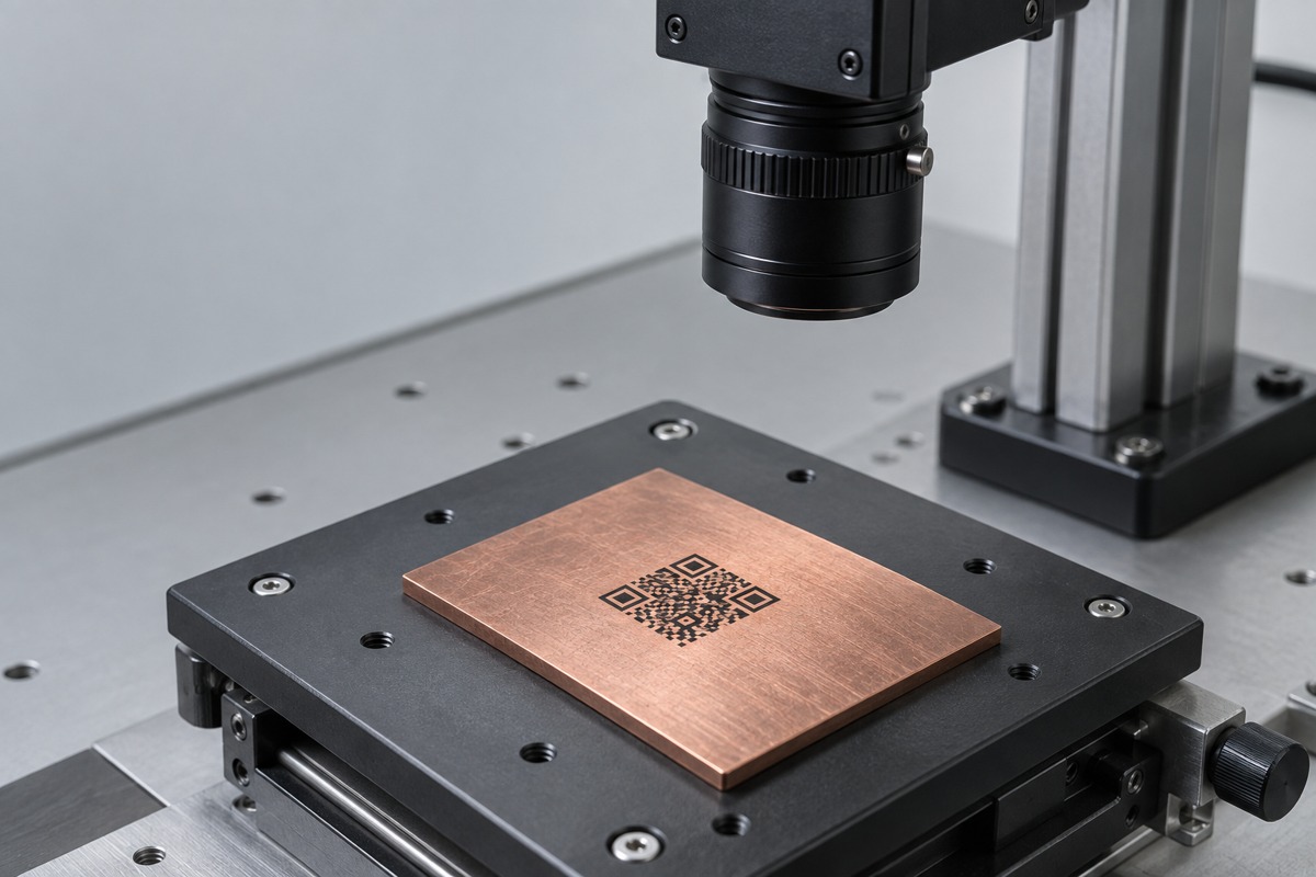
QR code marking on copper
AI illustration of optical inspection; no scan result is represented.

How Can PCB Laser Marking Support PCB and PCBA Traceability?

PCB laser marking gives production records a physical reference on the board. Its value to a buyer is being able to connect a delivered assembly or field return to the relevant manufacturing history.

Batch identification helps narrow an investigation. If a material lot or production batch is affected, linked records can help identify which boards belong to that group. The usefulness of the search depends on the records captured during production.

Individual identification supports board-specific history. A unique code can connect one assembly to its inspection results, test results, and rework events. For the example B260914001, the database holds those records; the symbol supplies the identifier used to find them.

PCB-to-PCBA handoff preserves continuity. The assembler needs to retain the fabricator’s identifier or map it to the assembly identifier. Otherwise, PCB fabrication history and assembly records may remain separate even though both operations use codes.

A manufacturing execution system, or MES, can manage these associations. The marker applies the identifier, the reader checks it, and the production system connects it to records. The QR code does not collect manufacturing data by itself; each relevant operation must record its results against the correct identifier. Smaller operations can use controlled records without a full MES, as long as each code retrieves the correct history.

For your next PCB or PCBA order, define what you need to retrieve when a board is scanned: a production batch, an individual test result, or a repair history. Then specify whether the code must remain accessible after assembly. These decisions help avoid an obscured code or a readable identifier that leads to incomplete records.

FAQs about QR code marking on copper

Can a QR code be marked directly on copper?

Yes. Laser marking can create a readable pattern directly on copper. The process must produce sufficient contrast without exceeding the surface change the part can tolerate. Thin PCB copper needs a different assessment from a solid copper part.

What is the minimum size for a QR code on copper?

There is no universal minimum. It depends on the encoded data, module size, marking accuracy, and reader resolution. Include a quiet zone four modules wide on every side when calculating the required area.

Will a copper QR code remain readable after surface finishing?

Not automatically. Plating or coating can change its appearance and contrast. Evaluate readability after the planned finishing sequence, using the intended reader and lighting conditions.

Does a QR code need an MES to support traceability?

No. Controlled records can support traceability without a full MES. Each identifier must remain linked to the correct production history. An MES can manage those associations, but the code itself does not collect production data.

Should every PCB have a different QR code?

Use a unique identifier when you need individual test results or rework history. A shared batch code can support batch-level tracking, while a fixed product code identifies the model rather than an individual board.

Discuss your PCB fabrication or assembly requirements with EBest Circuit (Best Technology) at sales@bestpcbs.com. Send your Gerber files and quantity, plus the BOM for assembly work, and describe the identification you need. State whether copper marking is mandatory or another board location is acceptable, so the proposed marking approach can be assessed as part of the order. You do not need to choose a laser before making an enquiry. Discuss QR code marking on copper requirements with your enquiry.

You may also like

Certified ISO 9001 PCB Manufacturer in China with Quality Control and Traceability
Tuesday, August 25th, 2026

EBest Circuit is a certified ISO 9001 PCB manufacturer in China supporting bare PCB fabrication, component sourcing, PCB assembly, inspection planning, traceability, and prototype-to-volume production. Buyers can qualify the company, manufacturing scope, technical capability, and order-specific quality records through one RFQ instead of treating the certificate as the only supplier-selection criterion.

Send your released PCB data, quantities, application requirements, acceptance criteria, and required records to sales@bestpcbs.com. EBest Circuit can return a manufacturability review and quotation that identifies the proposed construction, production scope, open engineering questions, inspection plan, and shipment documents.

ISO 9001 PCB manufacturer, quality engineer reviewing a PCB and controlled fabrication documents

What Does ISO 9001 Mean for a PCB Manufacturer?

ISO 9001 certification confirms that the manufacturer’s quality-management system has been independently audited within the legal entity, site, and service scope shown on the certificate. For a PCB order, that system should control requirements, files, approved materials, production instructions, inspection records, nonconformities, corrective actions, and changes.

  • Customer requirements: The quotation, engineering questions, approvals, and purchase order should be reviewed before production release so the build starts from one agreed requirement set.
  • Document control: Gerber or ODB++, drill, stackup, drawing, BOM, centroid, assembly, and test files need identifiable revisions and controlled release status.
  • Supplier control: Laminates, copper-clad materials, surface-finish chemistry, and purchased components should come from evaluated sources under defined acceptance controls.
  • Process control: Fabrication and assembly steps need work instructions, trained personnel, maintained equipment, and monitoring appropriate to the product risk.
  • Corrective action: When a nonconformity occurs, the manufacturer should contain affected material, determine cause, implement action, and verify that the action works.

ISO 9001 does not define the layer count, laminate, copper thickness, via structure, impedance tolerance, surface finish, IPC class, or test limits for an individual board. These product requirements still belong in the fabrication package, purchase order, and acceptance plan. The commercial value of certification is therefore a controlled route for executing the order, not a substitute for the order itself.

How Can Buyers Verify an ISO 9001 PCB Manufacturer’s Certificate?

Verify that the certificate covers the legal entity, production site, and service scope proposed for your PCB order. Record the standard reference, certification body, accreditation information, issue date, and validity status, then match the certified name and address to the quotation and manufacturing route.

ISO 9001 PCB manufacturer, quality team checking certificate identity and scope against a PCB supplier
Certificate Field Buyer Check Risk if Unclear
Legal Entity Match the certified name to the quotation, contract, and invoice entity. A related company may be certified while the contracting entity is outside the scope.
Certified Site Confirm that the fabrication or assembly location proposed for the order is covered. A headquarters certificate may not cover a separate production site.
Service Scope Check whether the wording covers relevant manufacturing or assembly activities. The certificate may apply to sales, design, or another service rather than the quoted process.
Standard and Validity Record the full standard reference and confirm current status with the issuer or an accredited database. An obsolete, suspended, or unverifiable certificate cannot support current qualification.
Certification Body Identify the issuing body and any stated accreditation. A certificate image alone may not establish independent, accredited certification.

ISO’s certification verification guidance explains that certification is performed by independent certification bodies, not by ISO itself. If the issuer, site, or scope cannot be verified, resolve the discrepancy before approving the supplier.

What PCB Manufacturing Capabilities Does EBest Circuit Provide?

EBest Circuit provides defined process ranges for FR4 and HDI fabrication, metal-core PCBs, and ceramic PCBs. Buyers evaluating an ISO 9001 PCB manufacturer can use the table below to screen layer count, board thickness, size, trace and space, hole diameter, aspect ratio, impedance, and thermal requirements before submitting the released stackup for an order-specific feasibility review.

Specification FR4 and HDI PCB MCPCB Ceramic PCB
Maximum Layers 32 layers 10 layers Thick film: 10 layers
DCB: 2 layers
Maximum Thickness 2 layers: 6.0 mm
4 layers and above: 8.0 mm
4.0 mm Thick film: 1.5 mm
DCB: 1 layer 1.3 mm; 2 layers 1.6 mm
Maximum Board Size 610 × 610 mm
100 × 1,300 mm
610 × 1,625 mm Thick film: 200 × 200 mm
DCB: 138 × 178 mm
Minimum Trace / Space Standard: 4/4 mil
HDI: 2/2 mil
6/6 mil Thick film: 6/8 mil
DCB: 12/12 mil
Minimum Hole Diameter Standard: 0.20 mm
HDI: 0.10 mm
0.30 mm 0.10 mm
Maximum Aspect Ratio 8:1 12:1 8:1
Impedance Control >50 Ω: ±10%
≤50 Ω: ±5 Ω
Not specified Not specified
Thermal Conductivity 0.30–0.45 W/m·K Standard: 0.8–1.5 W/m·K
High: 2.0–3.0 W/m·K
Al₂O₃: ≥24 W/m·K
AlN: ≥170 W/m·K

These values describe separate process limits and must not be combined into one assumed build. Submit the stackup, material system, copper distribution, via structure, board dimensions, tolerances, finish, quantity, and acceptance criteria for a marked-up feasibility response. For bare boards, IPC printed-board standards can supply product-level criteria when the purchase documents identify the applicable standard, revision, class, and exceptions.

How Does an ISO 9001 PCB Manufacturer Manage DFM and Engineering Changes?

DFM should convert manufacturing questions into approved, traceable decisions before CAM release. Verbal assumptions and uncontrolled email attachments increase the risk of building the correct data incorrectly or building an obsolete revision correctly.

Step 1: Establish the released input set. Identify the controlling Gerber or ODB++, drill, netlist, drawing, stackup, and order revision. The manufacturer should record receipt and stop release if file names, revision marks, or dimensions conflict.

Step 2: Review manufacturability against the proposed process. Check annular rings, copper-to-edge clearances, drill relationships, solder-mask openings, controlled-impedance structures, panel rails, and any special material or finish notes. Each question should reference the affected feature and proposed disposition.

Step 3: Obtain documented buyer approval. The approved engineering response should state whether the source data changes, whether the manufacturer applies a controlled CAM adjustment, and which revision becomes production authority. Silence must not be treated as approval.

Step 4: Lock the manufacturing dataset. After approval, release one controlled dataset to production and withdraw superseded files from use. If a later change arrives, repeat impact review for tooling, work in progress, materials, assembly files, and test data.

Step 5: Verify the first output. Compare initial-lot evidence with the released drawing and agreed checks. Record discrepancies and disposition before the same process is used for repeat orders or higher volume.

An ISO 9001 PCB manufacturer should retain the approved engineering response with the released production data so later lots can be checked against the same decision history.

How Does an ISO 9001 PCB Manufacturer Control PCB Quality During Production?

PCB quality control must connect the released data to material acceptance, process checks, product inspection, electrical verification, and shipment release. The RFQ should identify which controls are standard for the proposed route and which order-specific inspections or reports need additional planning.

  • Incoming control: Match laminates, copper-clad materials, solder mask, surface-finish inputs, and purchased components to approved specifications or alternatives before use.
  • CAM and process release: Release one approved dataset, stackup, tooling package, and traveler after engineering questions are closed.
  • In-process verification: Define the measurements or coupons used to monitor dimensions, drilling, plating, registration, solder mask, controlled impedance, and other order-critical features.
  • Bare-board inspection and test: State visual and dimensional criteria, electrical-test coverage, sampling, measurement locations, limits, and required report identity.
  • Assembly controls: When PCBA is included, identify incoming component checks, solder-paste inspection, AOI, X-ray, programming, or functional test only where the design and acceptance plan require them.
  • Release and change control: Link accepted lots and shipment documents to the approved revision, then require authorization for changes identified in the purchase agreement.

Electrical test confirms conductor-network continuity against the design data but does not replace dimensional, material, workmanship, or assembly checks. The inspection plan should therefore identify the risk addressed by each method and the evidence used for lot release.

How Does ISO 9001 Improve PCB Traceability and Production Consistency?

A controlled traceability plan connects the released revision, approved material, production route, inspection results, and shipped lot. Define the identification depth during quotation so the prototype records can become the controlled baseline for pilot and volume production.

ISO 9001 PCB manufacturer, PCB lots moving through AOI inspection and traceability record review
Order Stage Control Objective Expected Output
Prototype Confirm design feasibility, manufacturing assumptions, and inspection access. Resolved engineering questions, released files, and documented build observations
Pilot or Low Volume Verify repeatability, approved materials, process settings, and record completeness. Stable route, first-article results, controlled deviations, and production-ready documentation
Volume Production Maintain the released baseline while monitoring lots, changes, and nonconformities. Lot-linked inspection, test, release, and shipment records at the agreed level

Traceability depth should match the product and contractual risk. A commercial prototype may need basic lot and revision identification, while a regulated or high-reliability program may require material batches, process route, operator or equipment records, inspection results, deviations, and shipment identity. Ask the supplier to demonstrate how a reported defect would be traced to the affected lot and released data.

What Quality Documents Can You Request From an ISO 9001 PCB Manufacturer?

Request the records needed to approve the lot, investigate a failure, or demonstrate compliance with the purchase requirements. Each document should identify the order or lot, applicable revision, test or inspection method, result, and acceptance basis.

  • Certificate of conformance: Identify the purchase order, part number, revision, shipment lot, and requirement set covered by the declaration.
  • Electrical-test record: Define test coverage, method, netlist identity, result, and board or lot relationship for opens-and-shorts verification.
  • Visual and dimensional report: State the inspected drawing features, sampling, measured values, workmanship criteria, and acceptance limits.
  • Material evidence: Request laminate, copper, finish, or other material certificates only where material identity is contractually controlled.
  • Microsection or impedance report: When required, identify coupon or board location, measured features, target, tolerance, frequency, and acceptance result.
  • PCBA inspection or test record: For assembly orders, define applicable AOI, X-ray, programming, functional test, fixture, firmware, test limits, and result format.

The certificate of conformance should identify the order or lot and the applicable requirement set. If raw measurement data, material evidence or inspection images are required, include them in the RFQ so the supplier can plan record generation and retention.

How Much Does It Cost to Work With an ISO 9001 PCB Manufacturer?

ISO 9001 certification is not a standalone line-item price; cost and lead time are driven by the board, order scope and evidence package operated within the QMS. Incomplete or conflicting inputs cause quote revisions because the manufacturer cannot select a stable process and inspection plan.

Cost Driver Commercial Impact RFQ Input
Board Construction Layer count, material, copper, via structure, finish, and tolerances determine process steps and yield margin. Released stackup, fabrication drawing, and data package
Order Quantity Tooling, engineering, and setup are distributed differently across prototype and production quantities. Prototype, pilot, and forecast quantities
Inspection and Test Coupons, microsections, impedance, special sampling, fixtures, and reports add planned work. Method, frequency, limits, and required records
Documentation Customer-specific certificates, raw data, retention, and approval packages require preparation and review. Shipment-document checklist and retention period
Components and Assembly Availability, approved alternatives, package types, programming, and functional test affect the PCBA route. BOM, CPL, drawings, substitution rules, and test package
Schedule Material procurement, engineering closure, fabrication, sourcing, assembly, inspection, and transport have separate durations. Required delivery date and priorities

Compare quotations only after confirming that suppliers priced the same specifications, quantities, inspection scope, documentation, and delivery point. A lower quote based on missing records or an unapproved material assumption is not the same offer.

An ISO 9001 PCB manufacturer can quote more accurately when technical requirements and shipment records are defined before engineering review rather than added after production planning.

Why Choose EBest Circuit as Your ISO 9001 PCB Manufacturer in China?

EBest Circuit combines an ISO 9001:2015-certified quality system with PCB engineering, fabrication, component sourcing, assembly, and prototype-to-volume support in China. The advantage is a single manufacturing response that connects technical feasibility, production scope, quality records, and commercial quotation to the same released project.

  • Verified quality-system foundation: Buyers can review EBest Circuit’s ISO 9001:2015 certificate together with the legal entity, site, and service scope used for the order.
  • Defined fabrication ranges: The current matrix covers FR4 and HDI fabrication, metal-core PCBs, and ceramic PCBs, including board size, thickness, trace and space, hole, aspect-ratio, impedance, and thermal limits that can be checked against the released design.
  • One-stop PCB and PCBA scope: PCB design support, prototyping, fabrication, component sourcing, assembly, inspection planning, and shipment documentation can be coordinated through one supplier response.
  • Controlled DFM and release: Engineering questions, proposed manufacturing adjustments, approved revisions, and superseded data can be resolved before production release.
  • Prototype-to-volume continuity: Material, process, inspection, traceability, and document requirements can be identified during prototyping and retained as quantities increase.
  • Order-specific evidence: Certificates, inspection results, electrical-test records, material evidence, and PCBA test records can be quoted according to the actual acceptance package rather than assumed after shipment.

Request EBest Circuit’s current ISO 9001:2015 certificate together with a marked-up stackup, manufacturing route, inspection plan, traceability fields, and deliverable list. This gives engineering, procurement, and quality teams one comparable package for supplier approval and quotation review.

What Files Should You Send to an ISO 9001 PCB Manufacturer?

Send one revision-aligned package that defines the product, quantity, acceptance criteria and required deliverables. The manufacturer can then return specific engineering questions and a quote based on an identifiable scope.

  • Bare PCB: Gerber or ODB++, NC drill, netlist where available, fabrication drawing, stackup, controlled-impedance information, and panel requirements.
  • Optional assembly scope: If PCBA is included, add the BOM with approved manufacturer part numbers, centroid or pick-and-place data, assembly drawings, polarity notes, and special handling requirements.
  • Commercial: Prototype and production quantities, delivery destination, required date, and any forecast relevant to material planning.
  • Quality: Applicable standards and class, inspection and test methods, sampling or full-test requirements, traceability level, and deviation-approval route.
  • Deliverables: Certificate of conformance, test report, inspection data, material evidence, or other records required with the shipment.

If one item is not finalized, mark it as an open decision rather than leaving the supplier to infer it. The quotation should identify the assumption, its cost or schedule effect, and the approval needed before release.

FAQs About ISO 9001 PCB Manufacturers

Q1: Is ISO 9001 certification mandatory for every PCB purchase?

A1: Certification is required only when the contract, market, risk controls, or approved-supplier policy calls for it. When ISO 9001 is a sourcing requirement, identify the acceptable standard reference, legal entity, production site, service scope, and verification evidence before requesting or approving a quotation.

Q2: Can an ISO 9001 PCB manufacturer provide PCB assembly services?

A2: PCB assembly can be included when the supplier’s controlled scope supports the required PCBA processes. Confirm component sourcing, approved alternatives, workmanship criteria, inspection, programming, functional testing, traceability, and shipment records so the assembly quotation covers the complete acceptance package.

Q3: Does one ISO 9001 certificate cover every branch or factory?

A3: Coverage is limited to the entities and sites identified by the certificate and its scope. If quotation, fabrication, assembly, inspection, or shipment involves another location, request written confirmation of that site’s role, quality-system coverage, transferred requirements, and retained records before supplier approval.

Q4: Does ISO 9001 guarantee defect-free PCBs?

A4: ISO 9001 does not guarantee a defect-free PCB. Product conformity still depends on complete design inputs, capable manufacturing processes, appropriate inspection and testing, clear acceptance limits, and effective containment and corrective action when a nonconformity is found.

Q5: What certifications may matter in addition to ISO 9001?

A5: Additional credentials must match the market, product, and contract. Buyers may evaluate IATF 16949 for automotive supply chains, ISO 13485 for medical-device quality systems, AS9100D for aerospace quality management, UL recognition, RoHS, or REACH evidence where applicable. Verify the entity, site, scope, validity, and order relevance of each item.

Q6: Can the manufacturer substitute an equivalent laminate?

A6: A laminate substitution is acceptable only when the released requirements or buyer approval route permits it. The supplier should identify the proposed material, property comparison, stackup effect, impedance impact, availability, and approval status before purchasing or releasing the alternative to production.

Q7: How often should a supplier’s ISO 9001 certificate be rechecked?

A7: Recheck the certificate whenever its identity or validity may affect supplier approval. Minimum triggers include initial qualification, approaching expiry, a legal-entity or site change, a revised service scope, and the periodic interval defined by the approved-supplier program. Record the certificate identity, source, verification date, and reviewer.

Q8: Does an ISO 9001-certified supplier still need an initial-lot review?

A8: An initial-lot review remains necessary when the drawing, product risk, or buyer procedure requires it. The review checks whether the approved data, material, process route, inspection plan, and records produce an acceptable board before repeat orders or a higher-volume release.

Q9: Can a certificate of conformance replace detailed test reports?

A9: A certificate of conformance is sufficient only when the purchase agreement accepts it as the complete release evidence. If measured results, raw data, inspection images, impedance reports, or material certificates are required, list each document separately in the RFQ, quotation, and shipment-document checklist.

Q10: Who should approve a PCB manufacturing deviation?

A10: The buyer representative named by the contract or change-control procedure must approve the deviation. The documented disposition should identify the affected requirement, part and revision, quantity, lot, temporary or permanent status, acceptance rationale, expiry or review point, and required follow-up action.

Conclusion

EBest Circuit offers buyers a certified PCB manufacturing partner in China with defined process ranges for FR4 and HDI fabrication, metal-core PCBs, and ceramic PCBs, plus PCBA services, controlled engineering release, traceability, and order-specific records. The RFQ should connect the applicable process range to the exact board construction, quantities, acceptance criteria, changes, and evidence required for the project.

Send your Gerber or ODB++ package, drawing, stackup, BOM if assembly is required, quantities, acceptance criteria, and record list to sales@bestpcbs.com. Ask EBest Circuit for a marked-up manufacturing response, applicable certificate, inspection plan, and quotation tied to the released PCB or PCBA requirements.

You may also like

Printed Circuit Board Labels: PCB Marking, QR Codes & Traceability Guide
Wednesday, May 13th, 2026

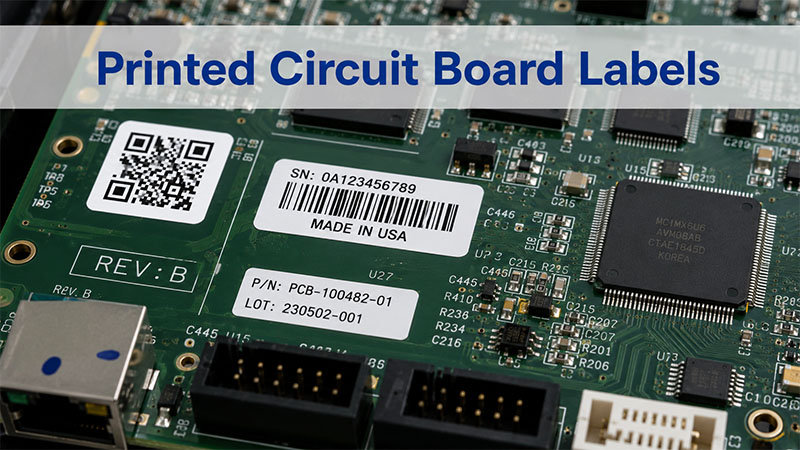
Printed circuit board labels are identification marks used on PCBs or PCB assemblies to show key information such as part numbers, revision codes, serial numbers, QR codes, barcodes, batch numbers, and inspection data. This article explains how PCB labels support board identification, traceability, quality control, and smarter production management in modern electronics manufacturing.

EBest Circuit (Best Technology) is an experienced PCB and PCBA manufacturer supporting customers with PCB fabrication, component sourcing, PCBA assembly, DFM review, testing, and traceability-focused production support. For projects that require printed circuit board labels, QR codes, serial numbers, batch tracking, or custom PCB identification, our engineering team can help review the labeling method, placement, material, and manufacturing process before production. If you are planning a PCB or PCBA project and want practical advice on labeling and traceability, pls feel free to contact us at sales@bestpcbs.com.

printed circuit board labels

What Are Printed Circuit Board Labels?

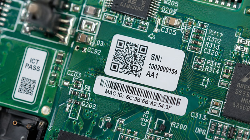
Printed circuit board labels help manufacturers identify, track, and manage PCBs during fabrication, assembly, testing, shipping, and after-sales support. A label can show a part number, revision code, batch number, serial number, QR code, barcode, or inspection mark.

In simple words, a PCB label works like an identity card for a circuit board. It tells engineers what the board is, where it came from, and which production record belongs to it.

A label may appear as silkscreen text, laser marking, a QR code, a barcode, or a high-temperature adhesive label. Each method serves a different purpose. For example, silkscreen works well for fixed text, while QR codes work better for traceability data.

Therefore, PCB labels do more than make a board look organized. They also help production teams control quality, reduce mix-ups, and find records faster.

Why Are Printed Circuit Board Labels Important?

PCB production involves many steps. Engineers need to check materials, boards, components, assembly data, inspection results, and shipment details. Without clear labels, teams may spend more time finding the right information.

That is why labels matter. They help link each board to a specific order, production batch, test result, or customer project. As a result, the whole manufacturing flow becomes easier to manage.

For example, two PCBs may look almost the same but belong to different revisions. A small revision code can help operators avoid using the wrong version. In addition, a QR code can connect the board to digital records in a manufacturing system.

For medical, automotive, industrial, communication, and aerospace electronics, this level of control becomes even more valuable. These products often need clear records and stable quality tracking.

What Information Should a PCB Label Include?

A PCB label should show the information that helps production, inspection, and future support. However, the label should not carry too much data. A crowded label becomes hard to read and hard to scan.

Common label information includes:

Label InformationMain Purpose
Part numberIdentifies the PCB or PCBA model
Revision codeShows the design version
Batch numberLinks the board to one production lot
Serial numberGives each board a unique identity
Date codeShows the production or assembly date
QR codeConnects the board to digital records
BarcodeSupports fast scanning in production
Inspection markShows quality control status
Customer codeMatches the board with customer records

For simple prototype boards, part number and revision code may be enough. However, production PCB assemblies often need serial numbers, QR codes, and batch tracking.

Also, the label format should stay consistent from batch to batch. Consistency helps engineers, quality teams, and customers read the data in the same way.

How Do Printed Circuit Board Labels Support Traceability?

Traceability means that a team can track a board through its full production history. Labels make this possible by giving each PCB a clear identity.

During PCB fabrication, the label may connect to material batch, panel number, surface finish, and production date. During PCBA assembly, the same board may also connect to solder paste batch, SMT line, component lots, AOI results, X-ray inspection, and final test data.

Therefore, if a quality issue appears later, engineers can scan the code and review the board’s history. This helps them find the source of the issue faster.

In addition, traceability supports inventory control. Warehouses can scan barcodes or QR codes when boards move through kitting, assembly, testing, packing, and shipping.

For customers, this creates more confidence. They receive boards with clear identity and better production records.

How Are Printed Circuit Board Labels Printed or Marked?

Manufacturers can print or mark PCB labels in several ways. The best method depends on the label content, board size, process temperature, and traceability needs.

  • Silkscreen marking is common in PCB fabrication. It shows component reference designators, polarity marks, logos, part numbers, and simple text. Because silkscreen works best for fixed information, it suits data that does not change from board to board.
  • Laser marking works well for QR codes, serial numbers, date codes, and permanent marks. The laser marks the board surface directly. As a result, the code will not peel off like an adhesive label.
  • Adhesive labels offer flexibility. Manufacturers can print barcodes, QR codes, serial numbers, and customer-specific data on them. However, the label material must suit heat, cleaning, and handling conditions.
  • Thermal transfer printing also supports variable data. Many factories use this method to print high-temperature PCB labels with clear barcodes and QR codes.

In many cases, manufacturers combine several methods. For example, a PCB may use silkscreen for fixed text and laser marking for a unique QR code.

Printed Circuit Board Labels vs Silkscreen Marking: What Is the Difference?

Silkscreen marking and PCB labels are related, but they do not mean the same thing.

Silkscreen refers to printed text and symbols on the PCB surface. It usually appears during the PCB fabrication process. Engineers use it for component names, polarity marks, connector labels, logos, and assembly guidance.

PCB labels cover a wider range. They may include silkscreen, laser marking, QR codes, barcodes, serial numbers, or adhesive labels. So, silkscreen can be part of PCB labeling, but it is not the only method.

ItemSilkscreen MarkingPCB Label
Main purposeAssembly guidanceIdentification and traceability
Common contentRef designators, polarity, logosSerial number, batch code, QR code
Variable dataLimitedStrong support
Process stagePCB fabricationFabrication, assembly, testing, or shipping
Best useVisual guidanceTracking and production control

In practice, both methods often work together. Silkscreen helps operators assemble the board. Meanwhile, labels help teams track the board through production and quality control.

Can Custom Printed Circuit Board Labels Include QR Codes?

Yes. Custom printed circuit board labels can include QR codes, barcodes, serial numbers, batch codes, and customer part numbers.

QR codes work especially well for modern PCB traceability. A small QR code can connect a board to a large amount of digital data. For example, it can link to production date, inspection results, component lots, test reports, firmware version, or shipment records.

This is useful because a PCB surface has limited space. Instead of printing long text on the board, a QR code can store or connect to the needed data.

However, engineers need to plan the QR code carefully. The code must have enough size, contrast, and open space around it. Otherwise, scanners may read it poorly.

Also, the code should stay visible after assembly. Components, heatsinks, connectors, batteries, cables, and enclosures may cover some areas. Therefore, label position matters as much as label content.

What Materials Are Used for PCB Labels?

PCB labels need stronger materials than ordinary paper labels. Electronics production may involve heat, soldering, cleaning, handling, and long-term operation.

  • Polyimide labels are popular for high-temperature PCB processes. They can handle heat better than many standard label materials. Because of this, manufacturers often use them for barcode and serial number labels.
  • Polyester labels suit many general electronics products. They offer clean print quality and stable appearance. However, engineers should check the exact temperature rating before use.
  • Laser marking does not add a separate label material. Instead, the laser creates a mark directly on the board surface. This method offers strong durability and a clean appearance.
  • Silkscreen ink works well for fixed markings. It can show board names, reference designators, polarity marks, and simple identification text.
  • Thermal transfer labels can produce clear QR codes and barcodes. They work well when paired with the right ribbon and label substrate.

The right material depends on the process. Therefore, engineers should consider temperature, cleaning chemicals, surface finish, and product environment before choosing the label type.

Where Should Labels Be Placed on a PCB?

Label placement affects readability and manufacturing efficiency. A good label should be easy to see, easy to scan, and safe from process problems.

In most cases, the label should sit on a flat area with enough open space. It should also avoid pads, vias, test points, mounting holes, and copper-exposed areas.

In addition, engineers should keep labels away from high-heat components when they use adhesive materials. Power devices, LED modules, transformers, and heatsinks may create heat that affects label life.

Visibility also matters. A label may look good in the PCB design file, but a connector or shield can cover it after assembly. Therefore, the team should review the final assembled structure.

For QR codes and barcodes, scanning angle and distance also matter. A code that looks clear to the eye may still fail in production scanning if it is too small or poorly placed.

That is why DFM review is helpful. A PCB manufacturer can check label position before fabrication and suggest better options.

How Do PCB Labels Improve Quality Control?

PCB labels help quality teams identify boards quickly and record inspection results accurately. This reduces confusion during production.

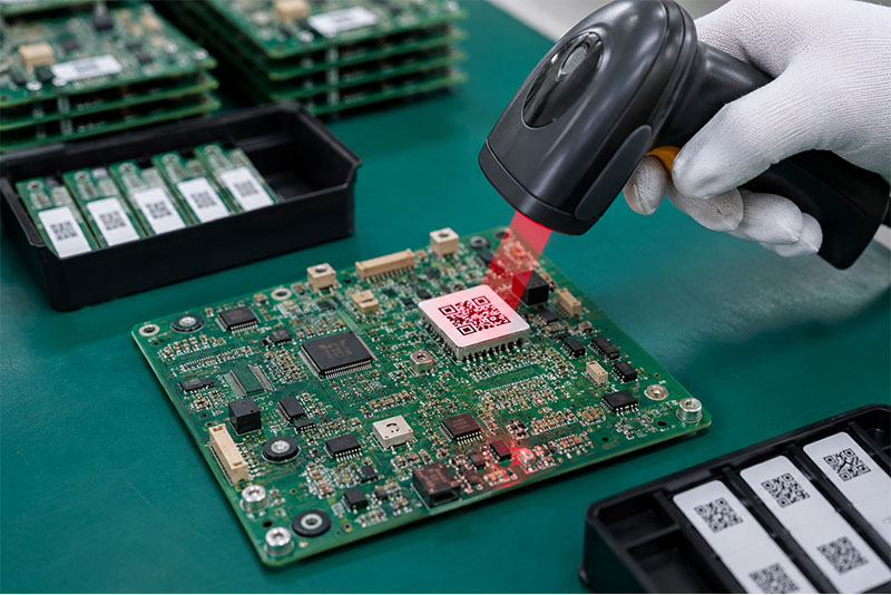
For example, operators can scan a barcode before SMT assembly. Then, the system can connect the board to solder paste batch, component lot, machine setup, and reflow profile.

After assembly, quality teams can scan the same code during AOI, X-ray inspection, ICT, functional testing, and final inspection. As a result, each board receives a clear quality record.

This process also helps when a board needs review. Engineers can check the serial number and see what happened during production. They can review test data, repair notes, or inspection images.

For customers, this creates a more transparent process. They can manage product versions, warranty records, and field feedback more easily.

In short, PCB labels turn a physical board into a traceable product. That makes quality control faster and more organized.

Which Industries Need Reliable PCB Labeling?

Many electronics industries use PCB labels. However, some sectors need stronger identification and traceability than others.

  • Medical electronics need clear tracking because device quality and documentation matter greatly. Labels help link each PCB assembly to production and inspection records.
  • Automotive electronics also rely on traceability. Control modules, sensors, lighting boards, and power electronics often need batch control and long-term records.
  • Industrial automation products may stay in service for many years. Clear labels help maintenance teams identify versions and replace parts correctly.
  • Communication equipment often includes different board revisions and test configurations. Labels help engineers manage these details.
  • Aerospace and UAV electronics usually need stable process control and detailed records. Labels support this need from prototype to production.

Even consumer electronics can benefit from labels. They help with inventory, warranty, repair, and shipment management.

Therefore, reliable labeling supports both high-end products and everyday electronics manufacturing.

How to Choose the Right Printed Circuit Board Labels

The best label choice depends on what the board needs to show and how the product will be used.

  • First, define the purpose. Do you need simple identification, batch tracking, serial number control, QR code scanning, or full traceability? This decision shapes the label method.
  • Next, check the process. If the board must pass through reflow soldering, choose a high-temperature label or laser marking. If the label only appears after final testing, an adhesive label may work well.
  • Then, review the environment. A PCB used in industrial power equipment may need a more durable label than a low-power consumer board.
  • Also, think about scanning. If the production line uses barcode or QR code scanners, the label must have the right size, contrast, and placement.

Here is a simple guide:

RequirementRecommended Method
Fixed text or logoSilkscreen
Unique serial numberLaser marking or printed label
QR code traceabilityLaser marking or high-resolution label
High-temperature processPolyimide label or laser marking
Long-term durabilityLaser marking
Low-cost board IDSilkscreen
Production scanningBarcode or QR code label

The best option is not always the most complex one. It is the method that stays readable and fits the manufacturing flow.

Why Choose an Experienced PCB Manufacturer for Printed Circuit Board Labels?

PCB labeling may seem like a small detail. However, it affects PCB design, fabrication, assembly, testing, packing, and traceability.

An experienced PCB manufacturer can review the label area during DFM checking. The team can confirm whether the label size, position, and marking method fit the board layout.

For example, if a QR code is too small, the manufacturer can suggest a larger size. If a label sits too close to a component, the engineer can move it before production. In addition, if the board needs high-temperature resistance, the supplier can suggest a better material.

For PCBA projects, timing also matters. Some labels should appear before SMT assembly. Others should appear after testing. The right sequence helps the factory track boards without slowing production.

EBest Circuit supports PCB fabrication, PCBA assembly, component sourcing, DFM review, testing, and production-quality support. For projects that need QR codes, serial numbers, custom labels, or traceability control, early communication helps build a smoother production process.

In a nutshell, printed circuit board labels help manufacturers identify boards, control revisions, track batches, manage QR codes, and improve traceability. They also support smoother production, faster inspection, and better after-sales support.

For simple PCBs, silkscreen may provide enough identification. For advanced PCB assemblies, serial numbers, QR codes, barcodes, and durable labels can create stronger process control.

Therefore, engineers should plan PCB labeling early. They should consider label content, material, marking method, placement, scanning needs, and long-term readability.

When the label strategy fits the product and process, every board becomes easier to track, inspect, ship, and support. If you are planning a PCB or PCBA project that requires custom labels, QR codes, serial numbers, or traceability support, feel free to contact EBest Circuit at sales@bestpcbs.com for practical manufacturing advice.

FAQs About Printed Circuit Board Labels

1. What is a printed circuit board label?
A printed circuit board label is an identification mark on a PCB or PCBA. It may show a part number, revision code, batch number, serial number, barcode, or QR code.

2. Are PCB labels the same as silkscreen?
No. Silkscreen is one marking method. PCB labels can also include laser marking, adhesive labels, QR codes, barcodes, and serial numbers.

3. Can a PCB label include a QR code?
Yes. A QR code can connect the board to production records, inspection results, component lots, test data, and shipment information.

4. What label material is best for PCB assembly?
Polyimide labels and laser marking work well for high-temperature processes. However, the best choice depends on temperature, cleaning method, and product use.

5. Where should a PCB label go?
A PCB label should sit in a flat, visible, and scannable area. It should avoid pads, vias, test points, holes, high-heat areas, and covered zones.

6. Do all PCBs need labels?
Most production PCBs need some form of identification. Simple boards may only need silkscreen text. Complex PCB assemblies may need QR codes and serial numbers.

7. Can custom PCB labels support mass production?
Yes. Custom labels can support batch tracking, unique serial numbers, QR codes, customer part numbers, warehouse scanning, and quality control.

8. Is laser marking better than adhesive labeling?
Laser marking offers strong durability and a clean surface. Adhesive labels offer more flexibility for printed data. The better choice depends on the board design and process.

You may also like