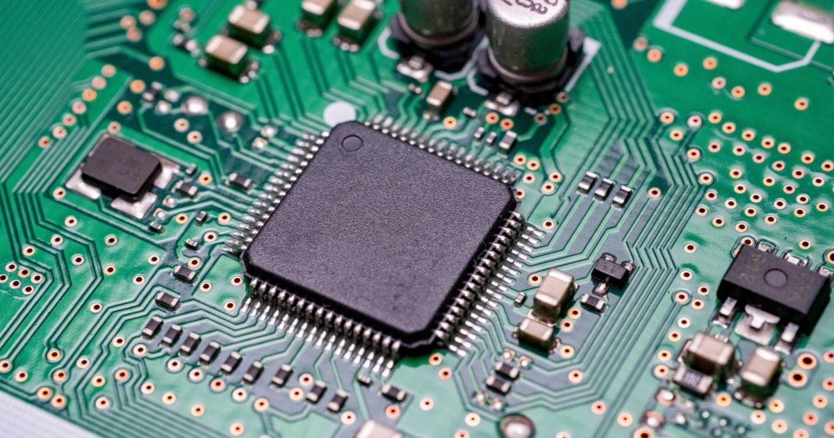
A PCB heat sink is effective only when the complete path from semiconductor junction to ambient air is controlled. A large finned part cannot compensate for a poor package interface, inadequate copper spreading, trapped air or uncontrolled mounting pressure. The practical design task is therefore to budget every thermal resistance, confirm mechanical compatibility and verify the assembled board under its worst credible operating condition.
This guide explains how designers and technical buyers can make that decision without treating a catalog heat-sink rating as a guaranteed board temperature. It covers top- and bottom-side paths, thermal interface materials, thermal vias, airflow, fabrication data and measurement. Select the cooling architecture from the device temperature limit and calculated total heat path, then validate it on the manufactured assembly.

What Is a PCB Heat Sink and How Does Heat Flow From the Component to the Ambient?
A PCB heat sink is a thermally conductive structure that spreads heat from a board-mounted source and increases the surface area available to the surrounding air. Heat first conducts from the semiconductor junction through its package. It then crosses a case, exposed pad or board interface, spreads through metal and finally leaves by convection and radiation. Each interface adds thermal resistance.
A top-mounted sink usually receives heat through the package case. A bottom-side sink may instead receive heat through an exposed pad, copper planes and thermal vias. Texas Instruments shows this board-through path in its thermal design guidance. Neither arrangement is universally superior: the correct path is the one supported by the package construction and layout.
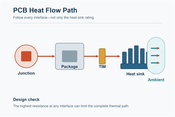
A larger heat sink cannot compensate for excessive thermal resistance at the interface. If a thick or poorly compressed thermal pad dominates the heat path, increasing the fin area will provide little improvement. Measure temperatures at the package, interface, heat-sink base, and ambient air, then compare the results with the calculated thermal-resistance chain.
When Does a PCB Need a Heat Sink?
A PCB needs a heat sink when the predicted junction temperature exceeds the allowable target after realistic copper spreading, airflow and operating duty are included. Start with maximum dissipated power, maximum local ambient temperature and the device temperature limit. Apply a design margin for unit variation, dust, fan aging, enclosure recirculation and uncertain interfaces.
Warning signs include protection trips at high load, a concentrated hot spot near a power package, unacceptable neighboring-component temperature or a calculated thermal budget that the bare board cannot meet. Power converters, motor drives, LED modules, processors and RF stages often deserve early analysis, but product category alone is not proof that a sink is required.
Use the datasheet thermal model only within its stated test conditions. A junction-to-ambient value measured on a reference board is not automatically transferable to a different stack-up or enclosure. Compare three candidates: improved board spreading, a board-plus-sink path and an alternative substrate. Choose the lowest-risk solution that meets temperature, space, cost, service and assembly constraints.
Is the Component Package Compatible With a Top-Mounted PCB Heat Sink?
Top mounting is acceptable only when the package manufacturer identifies a usable heat-transfer surface and the permitted mechanical load is compatible with the attachment. A plastic package top may not be the primary thermal path. Surface markings, mold draft, lid shape and nearby components can also prevent uniform contact.
Check the datasheet for junction-to-case definitions, exposed-pad intent, package coplanarity, maximum load and keep-out guidance. Confirm that the heat sink does not short leads, block connectors, interfere with rework or bridge components of different heights. Electrically conductive sinks may require an insulating TIM, but insulation increases thermal resistance and must be included in the budget.
When the exposed pad is the intended path, routing heat down through the board may be more reliable than pressing on the package top. Before layout release, obtain the package drawing, sink drawing, retention drawing and tolerance stack. A physical fit check should include the assembled solder height, not just nominal CAD bodies.
How Do You Calculate the Thermal-Resistance Budget for a PCB Heat Sink?
The maximum total thermal resistance equals the permitted junction-to-ambient temperature rise divided by worst-case power dissipation.
Rθ,total,max = (Tj,target – Ta,max) / Pd
For a case-mounted path, subtract the known junction-to-case and interface resistances to obtain the maximum allowable sink-to-ambient resistance:
Rθ,sa,max = (Tj,target – Ta,max) / Pd – Rθ,jc – Rθ,cs
Suppose a design target is 110°C, maximum local ambient is 50°C and dissipation is 6 W. The total budget is 10°C/W. If the applicable junction-to-case path is 2°C/W and the controlled interface is 1°C/W, the sink and its airflow must provide no more than 7°C/W. This is an illustrative calculation, not a part recommendation; the inputs must come from the selected device, TIM and actual environment.
For a bottom-side path, include package-to-pad, solder, via/plane spreading, board-to-sink interface and sink-to-air terms. Parallel heat paths may exist, but simple addition is valid only for the defined series branch. Analog Devices provides a useful thermal-circuit approach. Test sensitivity to power, ambient, interface resistance and airflow before committing to a marginal value.
What Types and Materials of PCB Heat Sinks Are Commonly Used?
Aluminum finned sinks are common because they balance conductivity, mass, manufacturability and cost, while copper is reserved for cases that justify greater spreading performance and weight. Fin spacing, base thickness, contact area, and mounting pressure can influence the assembled thermal resistance as strongly as the alloy choice.
- Stamped or formed sinks: light and economical for moderate loads, but thin bases may spread concentrated heat less effectively.
- Extruded aluminum sinks: provide repeatable fin geometry and many catalog profiles; cutting, drilling and finish must match the assembly drawing.
- Bonded, folded or skived-fin sinks: increase surface density where volume is constrained, but airflow pressure drop and cleanability require review.
- Board-level clip-on sinks: simplify assembly for compatible packages; retention force and package tolerance remain design inputs.
- Chassis-coupled spreaders: move heat to an enclosure wall. They can reduce local fin volume but make mechanical tolerances and user-touch temperature part of the design.
- Bottom-side heat spreaders: connect via fields or copper regions to a sink below the PCB. They keep the package top accessible but require a deliberate board path.
Surface finish can affect corrosion resistance, emissivity and electrical behavior, but it does not remove the need for flat contact. Specify whether the sink is electrically floating, grounded or insulated, and verify creepage and clearance around it.
How Do You Choose the Right PCB Heat Sink for Power, Size and Airflow?
Choose a heat sink by the required sink-to-ambient resistance at the actual airflow, then screen it for envelope, mass, attachment and manufacturing tolerance. A catalog rating is usable only when its orientation, air velocity and test method resemble the product.
| Selection input | What to specify | Failure if omitted | Verification |
|---|---|---|---|
| Thermal load | Worst-case loss, duty cycle and nearby heat sources | Sink sized to nominal rather than peak condition | Loss calculation and powered prototype |
| Ambient | Local inlet and recirculated-air temperature | Bench test understates enclosure temperature | Thermocouples at inlet and sink region |
| Airflow | Natural or forced flow, velocity range and direction | Catalog performance is not reproduced | Airflow measurement and fan-fault test |
| Envelope | XYZ clearance, keep-outs and service access | Collision, blocked connector or poor rework access | CAD tolerance review and first-article fit check |
| Attachment | Clip, adhesive, screw or chassis load path | Package damage or sink movement | Assembly-force control and mechanical inspection |
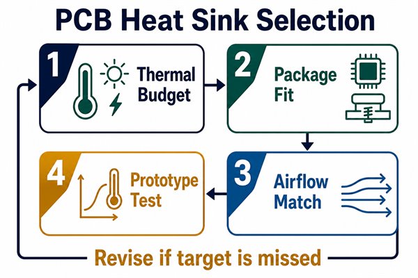
When airflow is uncertain, compare at least two fin profiles or orientations across the expected velocity range. Thermal simulation can identify sensitivities, but a manufactured prototype is still needed because contact quality, board warpage and enclosure leakage are difficult to predict accurately.
When Should You Use a Heat Sink Instead of Thermal Vias, MCPCB or Embedded Copper?
Use an external heat sink when the board alone cannot provide the required ambient interface or when heat must be moved to a controlled airflow or chassis surface. Use thermal vias and copper planes first when the package is designed to transfer heat through an exposed pad and the required spreading is achievable within a conventional multilayer board.
An MCPCB can shorten the path for surface-mounted heat sources distributed on one side, especially where electrical routing is comparatively simple. Embedded or thick copper can improve lateral spreading and current capacity, but it does not by itself guarantee low sink-to-air resistance. Complex multilayer interconnect, isolation requirements and component-side routing may favor a conventional PCB plus a defined external sink.
These approaches are often combined: an exposed pad, via array, internal copper, and bottom heat sink can form one continuous path. Compare total resistance, electrical isolation, layer count, assembly sequence, repairability, weight and supply risk. Do not select an alternative substrate from bulk conductivity alone; calculate the complete path and confirm that the stack-up and assembly process are manufacturable.
How Should a Heat Sink Be Mounted Without Damaging the PCB or Component?
The retention system should apply repeatable, balanced pressure through a load path that does not bend the package or PCB beyond their allowable limits. Screws, clips, push pins and adhesives each need an assembly specification rather than an operator judgment.
Step 1 — establish datum surfaces: start with the package drawing, PCB mechanical drawing and heat-sink contact geometry, then identify the thermal contact surface and the board, chassis or mounting holes that carry the retention load. Route that load through designed supports rather than component solder joints; document the load path in the assembly drawing and reject a layout that cannot show where the reaction force is carried.
Step 2 — review clearances: evaluate the complete tolerance stack in the 3D assembly, including leads, passives, connectors, creepage, routing keep-outs, fastener heads and tool access. Use the governing component drawing, insulation requirement and enclosure specification as the clearance sources; a worst-case interference or inaccessible fastener requires a layout or hardware change before the first article.
Step 3 — control the interface: release the exact TIM part number, placement pattern, bond-line or compressed thickness range and electrical-isolation requirement from the approved BOM and material data. Clean and inspect both contact surfaces before application because debris, trapped air, incomplete coverage or excessive material can increase interface resistance; record the first-article coverage or witness pattern and confirm required isolation before powering the assembly.
Step 4 — apply balanced retention: obtain the allowable package pressure or force from the device packaging guide and derive fastener torque, spring compression or clip force in the approved attachment drawing rather than using an operator-selected value. Tighten multi-point mounts in the released sequence while supporting the PCB so the sink remains parallel to the package; uneven loading can tilt the sink, bow the board or damage package corners. Record the controlled tool setting and verify the final gap or spring position against the assembly specification. AMD emphasizes planned mounting holes and controlled multi-point loading in its heat-sink mounting guidance.
Step 5 — inspect and test: use the released inspection plan to check sink seating, fastener engagement, board bow, electrical clearance and component damage before power is applied. Run the thermal verification at the defined dissipation, ambient, airflow and orientation, with measurement locations stated in the test plan; compare temperatures and mechanical measurements with the device limit and project acceptance criteria, then retain the results with the first-article record.
Heavy sinks also need shock and vibration review. The component solder joints should not become the only structural restraint. If adhesive is used, validate cure, bond-line thickness, aging, rework and compatibility with the package surface.
How Do TIM Thickness, Surface Flatness and Mounting Pressure Affect Heat Transfer?
A TIM should fill microscopic air gaps with the thinnest reliable bond line that the tolerance stack and insulation requirement permit. Increasing thickness usually increases resistance, while insufficient material or pressure leaves voids. Excessive pressure can bow the board, crack a package or squeeze material away from the interface.
Grease can create a thin interface but requires controlled application and lifecycle review. Pads simplify handling and can provide electrical isolation, but compression and thickness matter. Phase-change materials and adhesives solve different assembly problems and should not be substituted without new thermal and reliability validation.
Specify sink-base flatness, surface cleanliness, TIM placement and retention force as one system. Inspect witness patterns during development, but do not treat visual coverage as a thermal measurement. Re-test after thermal cycling when pump-out, settling or fastener relaxation is credible.
How Should Copper Areas, Thermal Vias and PCB Layout Work With a Heat Sink?
Copper and thermal vias must connect the device’s intended thermal pad to a sufficiently large spreading region and then to the heat sink without creating an assembly defect. Additional vias are useful only until the via-and-plane section is no longer a significant share of the total thermal resistance, and the selected construction must remain manufacturable.
Start from the component land-pattern recommendation. Specify via diameter, finished hole, pitch, plating, fill or cap requirement and connection to internal planes. Open vias in a solderable pad can wick solder and contribute to voiding; tenting or filling choices must match the assembly process. Analog Devices explains why an exposed paddle soldered to a land and connected into planes provides a lower-impedance path.
Maintain copper balance to limit bow, preserve electrical isolation and avoid splitting the thermal region with unnecessary voids. Keep heat-sensitive parts away from the exhaust side of the path. If the sink mounts below the board, include the board-to-sink contact area, solder-mask condition and component keep-out. Verify the final stack-up and via construction with the PCB fabricator before release.
How Do Airflow, Fin Orientation and Enclosure Design Affect PCB Heat Sink Performance?
Fins perform only when air can enter, travel along their channels and leave without recirculating hot exhaust back to the inlet. In natural convection, orient channels to support buoyant upward flow where the product orientation is known. In forced air, align fins with the actual stream and account for pressure drop.
A nearby wall, cable bundle or tall capacitor can block a nominally adequate sink. Multiple sinks can preheat one another. Fan specifications alone do not establish board-level velocity because vents, filters and leakage divide the flow. The relevant ambient is the air reaching the sink, not room temperature.
Measure inlet, outlet, sink base and critical component temperatures with the enclosure closed. Include low-line/high-line electrical conditions where they change loss, minimum fan speed, obstructed-filter or fan-fault states where required, and all intended product orientations.
What Heat Sink Requirements Should Be Defined in PCB Fabrication and Assembly Files?
The released data package must translate the thermal model into unambiguous board geometry, material, interface and assembly controls. A thermal intent note without dimensions or acceptance criteria is not sufficient.
| Document | Required heat-sink information | Independent check |
|---|---|---|
| PCB fabrication drawing | Stack-up, copper weights, via construction, fill/cap, tolerances, mounting holes and keep-outs | Fabricator DFM response matches the thermal path |
| Gerber/ODB++/IPC-2581 data | Thermal lands, solder-mask openings, plane connections and mechanical layers | CAM view agrees with drawing and land pattern |
| Assembly drawing | Sink orientation, hardware, insulators, TIM location, tightening sequence and torque/force | First article assembled using only released instructions |
| BOM | Exact sink, TIM, clip, washer, fastener and approved alternatives | Dimensions and material declarations are current |
| Inspection/test plan | Seating, bow, clearance, torque and thermal test conditions | Acceptance limits trace to design requirements |
Also identify electrically conductive surfaces and isolation requirements. Procurement should not approve a sink substitute from outer dimensions alone; base flatness, alloy, finish, fin geometry and mounting details may change performance.
How Should PCB Heat Sink Problems Be Diagnosed and Thermal Performance Be Verified?
Diagnose the thermal path node by node under controlled power, ambient and airflow rather than replacing the heat sink first. A hot junction with a relatively cool sink often indicates a poor interface or internal board bottleneck; a uniformly hot sink may indicate insufficient airflow or surface area.
Step 1 — reproduce the condition: rebuild the reported operating state using the recorded power loss, local ambient, enclosure configuration, board orientation and fan command. Hold these inputs long enough to reach the stability criterion in the test plan; otherwise two runs may appear different because of setup or warm-up variation rather than a design change. Save the complete condition log with the baseline temperature result.
Step 2 — verify instrumentation: select calibrated thermocouples, embedded sensors or infrared equipment that can resolve the expected temperature difference, and place each sensor at the location defined by the device vendor or test plan. Control infrared emissivity and route contact probes so they do not create a meaningful heat path; repeat a baseline reading to confirm stable, plausible measurements before diagnosing the assembly.
Step 3 — map temperatures: measure the package or vendor-defined proxy point, accessible PCB spreading region, sink base, fin region, air inlet and exhaust under the same stabilized load. Compare the temperature differences between adjacent nodes with the calculated thermal path; an unexplained large drop identifies where interface contact, board spreading or airflow requires further inspection. Retain the temperature map and measurement locations for comparison after each change.
Step 4 — isolate variables: change one controlled factor at a time, such as TIM application, airflow, sink orientation or mounting force—while holding power, ambient and the remaining assembly conditions constant. Changing several factors together can hide the true cause; repeat the baseline and modified run, then compare the measured change with the predicted sensitivity before accepting the diagnosis.
Step 5 — confirm production controls: use the released drawing, BOM and inspection plan to check TIM identity and coverage, fastener or spring condition, board bow, component identity and relevant assembly defects across the sample quantity defined by the quality plan. A single good unit cannot establish process control; record the distribution and disposition any unit that fails the mechanical or thermal acceptance criteria.
Step 6 — repeat at worst case: establish maximum credible power, ambient, airflow restriction, orientation, aging state and applicable fault conditions from the product risk assessment rather than inventing a generic stress point. Run the stabilized test with the same sensor locations and compare the result with the component temperature limit and product margin requirement; release the design only when the worst-case report, deviations and corrective actions are approved.
FAQs About PCB Heat Sinks
Q1: Can a heat sink be attached directly to a PCB?
A1: Yes, if designed mounting points carry the load and the interface reaches an intended board heat-spreading region. Do not rely on the hot component’s solder joints to support a heavy sink.
Q2: Are thermal vias enough without a heat sink?
A2: They can be enough when the completed board-to-air resistance meets the junction-temperature target. Their effectiveness depends on via construction, copper spreading, board thickness and airflow.
Q3: Can thermal paste replace a thermal pad?
A3: Not automatically. Paste may reduce bond-line thickness, but it may not provide the electrical isolation, gap tolerance, handling or lifecycle behavior required by the design.
Q4: Should heat-sink fins be vertical?
A4: For natural convection, channels should support unobstructed upward air movement in the intended product orientation. Forced-air designs should align them with measured flow.
Q5: Does a larger PCB heat sink always cool better?
A5: No. Added size brings little benefit when the package interface, board path or airflow is the dominant resistance.
Q6: How do I know whether the heat sink is working?
A6: Confirm that the junction or validated proxy remains below its design target under worst-case power, local ambient and airflow. Also verify mounting stability and neighboring-component temperatures.
Q7: Does a hot heat sink mean the design is failing?
A7: Not by itself. A warm sink can show that heat is crossing the interface successfully. Judge the design from the junction limit, local ambient, airflow and neighboring-component temperatures rather than sink temperature alone.
Q8: Is there a universal mounting torque for PCB heat sinks?
A8: No universal torque is safe for every package and retention system. Use the device, heat-sink and fastener specifications, then verify seating, board bow and interface compression on the assembled tolerance stack.
Q9: Must an aluminum PCB heat sink be electrically grounded?
A9: Grounding or isolation depends on the electrical architecture and safety requirements. Confirm clearances, accessible-metal requirements and whether the TIM provides verified electrical insulation before releasing the mounting design.
Q10: Should the thermal interface be rechecked after environmental testing?
A10: Yes, when cycling, vibration, aging or fastener relaxation can change contact pressure or TIM condition. Repeat the relevant temperature measurements and inspect retention, seating and interface evidence after the defined stress sequence.
Conclusion
Before releasing your PCB heat sink design for fabrication, send EBest Circuit the Gerber/ODB++ files, stack-up, BOM, component loss estimates, heat-sink drawing, TIM specification, enclosure constraints, expected airflow and thermal acceptance limits. These inputs allow the engineering review to identify unresolved copper-distribution, thermal-via, mounting and assembly requirements that affect manufacturability and quotation. Email sales@bestpcbs.com to request a PCB fabrication and assembly quotation.