PCB manufacturing PCB manufacturing
Home > Blog

PCB Thermal Management

PCB Heat Sink: Design, Selection and Thermal Testing
Tuesday, August 18th, 2026

A PCB heat sink is effective only when the complete path from semiconductor junction to ambient air is controlled. A large finned part cannot compensate for a poor package interface, inadequate copper spreading, trapped air or uncontrolled mounting pressure. The practical design task is therefore to budget every thermal resistance, confirm mechanical compatibility and verify the assembled board under its worst credible operating condition.

This guide explains how designers and technical buyers can make that decision without treating a catalog heat-sink rating as a guaranteed board temperature. It covers top- and bottom-side paths, thermal interface materials, thermal vias, airflow, fabrication data and measurement. Select the cooling architecture from the device temperature limit and calculated total heat path, then validate it on the manufactured assembly.

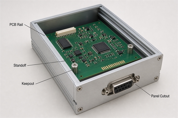
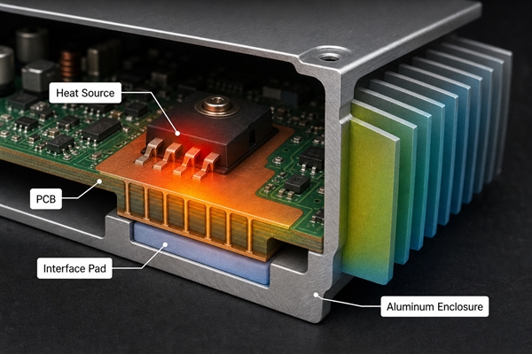
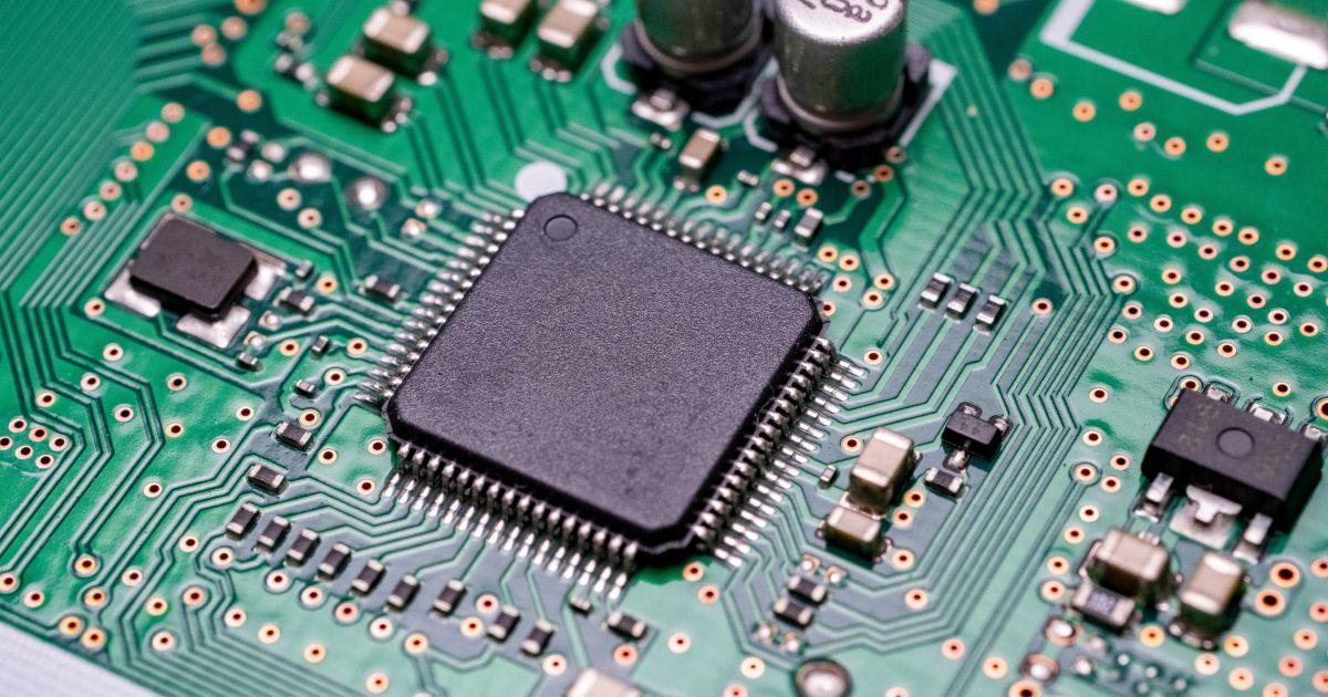
Populated printed circuit board with a finned aluminum heat sink mounted over a power component

What Is a PCB Heat Sink and How Does Heat Flow From the Component to the Ambient?

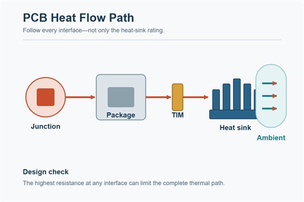
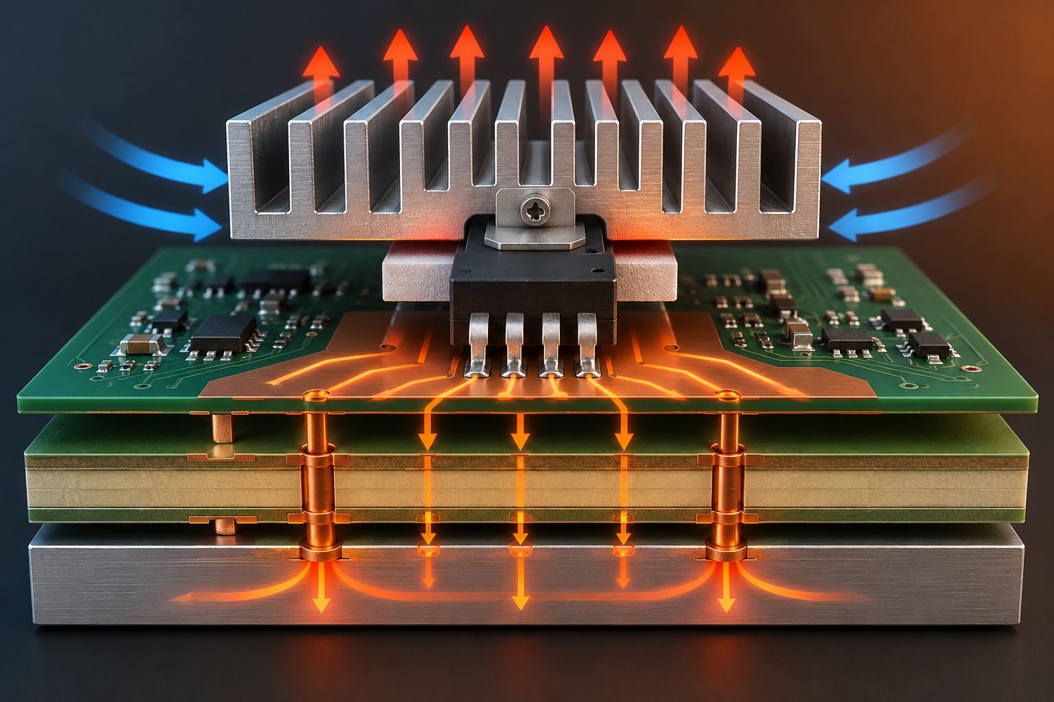
A PCB heat sink is a thermally conductive structure that spreads heat from a board-mounted source and increases the surface area available to the surrounding air. Heat first conducts from the semiconductor junction through its package. It then crosses a case, exposed pad or board interface, spreads through metal and finally leaves by convection and radiation. Each interface adds thermal resistance.

A top-mounted sink usually receives heat through the package case. A bottom-side sink may instead receive heat through an exposed pad, copper planes and thermal vias. Texas Instruments shows this board-through path in its thermal design guidance. Neither arrangement is universally superior: the correct path is the one supported by the package construction and layout.

Diagram showing heat flowing from a semiconductor junction through the package and heat sink to ambient air

A larger heat sink cannot compensate for excessive thermal resistance at the interface. If a thick or poorly compressed thermal pad dominates the heat path, increasing the fin area will provide little improvement. Measure temperatures at the package, interface, heat-sink base, and ambient air, then compare the results with the calculated thermal-resistance chain.

When Does a PCB Need a Heat Sink?

A PCB needs a heat sink when the predicted junction temperature exceeds the allowable target after realistic copper spreading, airflow and operating duty are included. Start with maximum dissipated power, maximum local ambient temperature and the device temperature limit. Apply a design margin for unit variation, dust, fan aging, enclosure recirculation and uncertain interfaces.

Warning signs include protection trips at high load, a concentrated hot spot near a power package, unacceptable neighboring-component temperature or a calculated thermal budget that the bare board cannot meet. Power converters, motor drives, LED modules, processors and RF stages often deserve early analysis, but product category alone is not proof that a sink is required.

Use the datasheet thermal model only within its stated test conditions. A junction-to-ambient value measured on a reference board is not automatically transferable to a different stack-up or enclosure. Compare three candidates: improved board spreading, a board-plus-sink path and an alternative substrate. Choose the lowest-risk solution that meets temperature, space, cost, service and assembly constraints.

Is the Component Package Compatible With a Top-Mounted PCB Heat Sink?

Top mounting is acceptable only when the package manufacturer identifies a usable heat-transfer surface and the permitted mechanical load is compatible with the attachment. A plastic package top may not be the primary thermal path. Surface markings, mold draft, lid shape and nearby components can also prevent uniform contact.

Check the datasheet for junction-to-case definitions, exposed-pad intent, package coplanarity, maximum load and keep-out guidance. Confirm that the heat sink does not short leads, block connectors, interfere with rework or bridge components of different heights. Electrically conductive sinks may require an insulating TIM, but insulation increases thermal resistance and must be included in the budget.

When the exposed pad is the intended path, routing heat down through the board may be more reliable than pressing on the package top. Before layout release, obtain the package drawing, sink drawing, retention drawing and tolerance stack. A physical fit check should include the assembled solder height, not just nominal CAD bodies.

How Do You Calculate the Thermal-Resistance Budget for a PCB Heat Sink?

The maximum total thermal resistance equals the permitted junction-to-ambient temperature rise divided by worst-case power dissipation.

Rθ,total,max = (Tj,target – Ta,max) / Pd

For a case-mounted path, subtract the known junction-to-case and interface resistances to obtain the maximum allowable sink-to-ambient resistance:

Rθ,sa,max = (Tj,target – Ta,max) / Pd – Rθ,jc – Rθ,cs

Suppose a design target is 110°C, maximum local ambient is 50°C and dissipation is 6 W. The total budget is 10°C/W. If the applicable junction-to-case path is 2°C/W and the controlled interface is 1°C/W, the sink and its airflow must provide no more than 7°C/W. This is an illustrative calculation, not a part recommendation; the inputs must come from the selected device, TIM and actual environment.

For a bottom-side path, include package-to-pad, solder, via/plane spreading, board-to-sink interface and sink-to-air terms. Parallel heat paths may exist, but simple addition is valid only for the defined series branch. Analog Devices provides a useful thermal-circuit approach. Test sensitivity to power, ambient, interface resistance and airflow before committing to a marginal value.

What Types and Materials of PCB Heat Sinks Are Commonly Used?

Aluminum finned sinks are common because they balance conductivity, mass, manufacturability and cost, while copper is reserved for cases that justify greater spreading performance and weight. Fin spacing, base thickness, contact area, and mounting pressure can influence the assembled thermal resistance as strongly as the alloy choice.

  • Stamped or formed sinks: light and economical for moderate loads, but thin bases may spread concentrated heat less effectively.
  • Extruded aluminum sinks: provide repeatable fin geometry and many catalog profiles; cutting, drilling and finish must match the assembly drawing.
  • Bonded, folded or skived-fin sinks: increase surface density where volume is constrained, but airflow pressure drop and cleanability require review.
  • Board-level clip-on sinks: simplify assembly for compatible packages; retention force and package tolerance remain design inputs.
  • Chassis-coupled spreaders: move heat to an enclosure wall. They can reduce local fin volume but make mechanical tolerances and user-touch temperature part of the design.
  • Bottom-side heat spreaders: connect via fields or copper regions to a sink below the PCB. They keep the package top accessible but require a deliberate board path.

Surface finish can affect corrosion resistance, emissivity and electrical behavior, but it does not remove the need for flat contact. Specify whether the sink is electrically floating, grounded or insulated, and verify creepage and clearance around it.

How Do You Choose the Right PCB Heat Sink for Power, Size and Airflow?

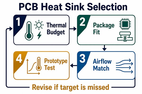
Choose a heat sink by the required sink-to-ambient resistance at the actual airflow, then screen it for envelope, mass, attachment and manufacturing tolerance. A catalog rating is usable only when its orientation, air velocity and test method resemble the product.

Selection input What to specify Failure if omitted Verification
Thermal load Worst-case loss, duty cycle and nearby heat sources Sink sized to nominal rather than peak condition Loss calculation and powered prototype
Ambient Local inlet and recirculated-air temperature Bench test understates enclosure temperature Thermocouples at inlet and sink region
Airflow Natural or forced flow, velocity range and direction Catalog performance is not reproduced Airflow measurement and fan-fault test
Envelope XYZ clearance, keep-outs and service access Collision, blocked connector or poor rework access CAD tolerance review and first-article fit check
Attachment Clip, adhesive, screw or chassis load path Package damage or sink movement Assembly-force control and mechanical inspection
Four-stage PCB heat sink selection process from thermal budget through prototype measurement

When airflow is uncertain, compare at least two fin profiles or orientations across the expected velocity range. Thermal simulation can identify sensitivities, but a manufactured prototype is still needed because contact quality, board warpage and enclosure leakage are difficult to predict accurately.

When Should You Use a Heat Sink Instead of Thermal Vias, MCPCB or Embedded Copper?

Use an external heat sink when the board alone cannot provide the required ambient interface or when heat must be moved to a controlled airflow or chassis surface. Use thermal vias and copper planes first when the package is designed to transfer heat through an exposed pad and the required spreading is achievable within a conventional multilayer board.

An MCPCB can shorten the path for surface-mounted heat sources distributed on one side, especially where electrical routing is comparatively simple. Embedded or thick copper can improve lateral spreading and current capacity, but it does not by itself guarantee low sink-to-air resistance. Complex multilayer interconnect, isolation requirements and component-side routing may favor a conventional PCB plus a defined external sink.

These approaches are often combined: an exposed pad, via array, internal copper, and bottom heat sink can form one continuous path. Compare total resistance, electrical isolation, layer count, assembly sequence, repairability, weight and supply risk. Do not select an alternative substrate from bulk conductivity alone; calculate the complete path and confirm that the stack-up and assembly process are manufacturable.

How Should a Heat Sink Be Mounted Without Damaging the PCB or Component?

The retention system should apply repeatable, balanced pressure through a load path that does not bend the package or PCB beyond their allowable limits. Screws, clips, push pins and adhesives each need an assembly specification rather than an operator judgment.

Step 1 — establish datum surfaces: start with the package drawing, PCB mechanical drawing and heat-sink contact geometry, then identify the thermal contact surface and the board, chassis or mounting holes that carry the retention load. Route that load through designed supports rather than component solder joints; document the load path in the assembly drawing and reject a layout that cannot show where the reaction force is carried.

Step 2 — review clearances: evaluate the complete tolerance stack in the 3D assembly, including leads, passives, connectors, creepage, routing keep-outs, fastener heads and tool access. Use the governing component drawing, insulation requirement and enclosure specification as the clearance sources; a worst-case interference or inaccessible fastener requires a layout or hardware change before the first article.

Step 3 — control the interface: release the exact TIM part number, placement pattern, bond-line or compressed thickness range and electrical-isolation requirement from the approved BOM and material data. Clean and inspect both contact surfaces before application because debris, trapped air, incomplete coverage or excessive material can increase interface resistance; record the first-article coverage or witness pattern and confirm required isolation before powering the assembly.

Step 4 — apply balanced retention: obtain the allowable package pressure or force from the device packaging guide and derive fastener torque, spring compression or clip force in the approved attachment drawing rather than using an operator-selected value. Tighten multi-point mounts in the released sequence while supporting the PCB so the sink remains parallel to the package; uneven loading can tilt the sink, bow the board or damage package corners. Record the controlled tool setting and verify the final gap or spring position against the assembly specification. AMD emphasizes planned mounting holes and controlled multi-point loading in its heat-sink mounting guidance.

Step 5 — inspect and test: use the released inspection plan to check sink seating, fastener engagement, board bow, electrical clearance and component damage before power is applied. Run the thermal verification at the defined dissipation, ambient, airflow and orientation, with measurement locations stated in the test plan; compare temperatures and mechanical measurements with the device limit and project acceptance criteria, then retain the results with the first-article record.

Heavy sinks also need shock and vibration review. The component solder joints should not become the only structural restraint. If adhesive is used, validate cure, bond-line thickness, aging, rework and compatibility with the package surface.

How Do TIM Thickness, Surface Flatness and Mounting Pressure Affect Heat Transfer?

A TIM should fill microscopic air gaps with the thinnest reliable bond line that the tolerance stack and insulation requirement permit. Increasing thickness usually increases resistance, while insufficient material or pressure leaves voids. Excessive pressure can bow the board, crack a package or squeeze material away from the interface.

Grease can create a thin interface but requires controlled application and lifecycle review. Pads simplify handling and can provide electrical isolation, but compression and thickness matter. Phase-change materials and adhesives solve different assembly problems and should not be substituted without new thermal and reliability validation.

Specify sink-base flatness, surface cleanliness, TIM placement and retention force as one system. Inspect witness patterns during development, but do not treat visual coverage as a thermal measurement. Re-test after thermal cycling when pump-out, settling or fastener relaxation is credible.

How Should Copper Areas, Thermal Vias and PCB Layout Work With a Heat Sink?

Copper and thermal vias must connect the device’s intended thermal pad to a sufficiently large spreading region and then to the heat sink without creating an assembly defect. Additional vias are useful only until the via-and-plane section is no longer a significant share of the total thermal resistance, and the selected construction must remain manufacturable.

Start from the component land-pattern recommendation. Specify via diameter, finished hole, pitch, plating, fill or cap requirement and connection to internal planes. Open vias in a solderable pad can wick solder and contribute to voiding; tenting or filling choices must match the assembly process. Analog Devices explains why an exposed paddle soldered to a land and connected into planes provides a lower-impedance path.

Maintain copper balance to limit bow, preserve electrical isolation and avoid splitting the thermal region with unnecessary voids. Keep heat-sensitive parts away from the exhaust side of the path. If the sink mounts below the board, include the board-to-sink contact area, solder-mask condition and component keep-out. Verify the final stack-up and via construction with the PCB fabricator before release.

How Do Airflow, Fin Orientation and Enclosure Design Affect PCB Heat Sink Performance?

Fins perform only when air can enter, travel along their channels and leave without recirculating hot exhaust back to the inlet. In natural convection, orient channels to support buoyant upward flow where the product orientation is known. In forced air, align fins with the actual stream and account for pressure drop.

A nearby wall, cable bundle or tall capacitor can block a nominally adequate sink. Multiple sinks can preheat one another. Fan specifications alone do not establish board-level velocity because vents, filters and leakage divide the flow. The relevant ambient is the air reaching the sink, not room temperature.

Measure inlet, outlet, sink base and critical component temperatures with the enclosure closed. Include low-line/high-line electrical conditions where they change loss, minimum fan speed, obstructed-filter or fan-fault states where required, and all intended product orientations.

What Heat Sink Requirements Should Be Defined in PCB Fabrication and Assembly Files?

The released data package must translate the thermal model into unambiguous board geometry, material, interface and assembly controls. A thermal intent note without dimensions or acceptance criteria is not sufficient.

Document Required heat-sink information Independent check
PCB fabrication drawing Stack-up, copper weights, via construction, fill/cap, tolerances, mounting holes and keep-outs Fabricator DFM response matches the thermal path
Gerber/ODB++/IPC-2581 data Thermal lands, solder-mask openings, plane connections and mechanical layers CAM view agrees with drawing and land pattern
Assembly drawing Sink orientation, hardware, insulators, TIM location, tightening sequence and torque/force First article assembled using only released instructions
BOM Exact sink, TIM, clip, washer, fastener and approved alternatives Dimensions and material declarations are current
Inspection/test plan Seating, bow, clearance, torque and thermal test conditions Acceptance limits trace to design requirements

Also identify electrically conductive surfaces and isolation requirements. Procurement should not approve a sink substitute from outer dimensions alone; base flatness, alloy, finish, fin geometry and mounting details may change performance.

How Should PCB Heat Sink Problems Be Diagnosed and Thermal Performance Be Verified?

Diagnose the thermal path node by node under controlled power, ambient and airflow rather than replacing the heat sink first. A hot junction with a relatively cool sink often indicates a poor interface or internal board bottleneck; a uniformly hot sink may indicate insufficient airflow or surface area.

Step 1 — reproduce the condition: rebuild the reported operating state using the recorded power loss, local ambient, enclosure configuration, board orientation and fan command. Hold these inputs long enough to reach the stability criterion in the test plan; otherwise two runs may appear different because of setup or warm-up variation rather than a design change. Save the complete condition log with the baseline temperature result.

Step 2 — verify instrumentation: select calibrated thermocouples, embedded sensors or infrared equipment that can resolve the expected temperature difference, and place each sensor at the location defined by the device vendor or test plan. Control infrared emissivity and route contact probes so they do not create a meaningful heat path; repeat a baseline reading to confirm stable, plausible measurements before diagnosing the assembly.

Step 3 — map temperatures: measure the package or vendor-defined proxy point, accessible PCB spreading region, sink base, fin region, air inlet and exhaust under the same stabilized load. Compare the temperature differences between adjacent nodes with the calculated thermal path; an unexplained large drop identifies where interface contact, board spreading or airflow requires further inspection. Retain the temperature map and measurement locations for comparison after each change.

Step 4 — isolate variables: change one controlled factor at a time, such as TIM application, airflow, sink orientation or mounting force—while holding power, ambient and the remaining assembly conditions constant. Changing several factors together can hide the true cause; repeat the baseline and modified run, then compare the measured change with the predicted sensitivity before accepting the diagnosis.

Step 5 — confirm production controls: use the released drawing, BOM and inspection plan to check TIM identity and coverage, fastener or spring condition, board bow, component identity and relevant assembly defects across the sample quantity defined by the quality plan. A single good unit cannot establish process control; record the distribution and disposition any unit that fails the mechanical or thermal acceptance criteria.

Step 6 — repeat at worst case: establish maximum credible power, ambient, airflow restriction, orientation, aging state and applicable fault conditions from the product risk assessment rather than inventing a generic stress point. Run the stabilized test with the same sensor locations and compare the result with the component temperature limit and product margin requirement; release the design only when the worst-case report, deviations and corrective actions are approved.

FAQs About PCB Heat Sinks

Q1: Can a heat sink be attached directly to a PCB?

A1: Yes, if designed mounting points carry the load and the interface reaches an intended board heat-spreading region. Do not rely on the hot component’s solder joints to support a heavy sink.

Q2: Are thermal vias enough without a heat sink?

A2: They can be enough when the completed board-to-air resistance meets the junction-temperature target. Their effectiveness depends on via construction, copper spreading, board thickness and airflow.

Q3: Can thermal paste replace a thermal pad?

A3: Not automatically. Paste may reduce bond-line thickness, but it may not provide the electrical isolation, gap tolerance, handling or lifecycle behavior required by the design.

Q4: Should heat-sink fins be vertical?

A4: For natural convection, channels should support unobstructed upward air movement in the intended product orientation. Forced-air designs should align them with measured flow.

Q5: Does a larger PCB heat sink always cool better?

A5: No. Added size brings little benefit when the package interface, board path or airflow is the dominant resistance.

Q6: How do I know whether the heat sink is working?

A6: Confirm that the junction or validated proxy remains below its design target under worst-case power, local ambient and airflow. Also verify mounting stability and neighboring-component temperatures.

Q7: Does a hot heat sink mean the design is failing?

A7: Not by itself. A warm sink can show that heat is crossing the interface successfully. Judge the design from the junction limit, local ambient, airflow and neighboring-component temperatures rather than sink temperature alone.

Q8: Is there a universal mounting torque for PCB heat sinks?

A8: No universal torque is safe for every package and retention system. Use the device, heat-sink and fastener specifications, then verify seating, board bow and interface compression on the assembled tolerance stack.

Q9: Must an aluminum PCB heat sink be electrically grounded?

A9: Grounding or isolation depends on the electrical architecture and safety requirements. Confirm clearances, accessible-metal requirements and whether the TIM provides verified electrical insulation before releasing the mounting design.

Q10: Should the thermal interface be rechecked after environmental testing?

A10: Yes, when cycling, vibration, aging or fastener relaxation can change contact pressure or TIM condition. Repeat the relevant temperature measurements and inspect retention, seating and interface evidence after the defined stress sequence.

Conclusion

Before releasing your PCB heat sink design for fabrication, send EBest Circuit the Gerber/ODB++ files, stack-up, BOM, component loss estimates, heat-sink drawing, TIM specification, enclosure constraints, expected airflow and thermal acceptance limits. These inputs allow the engineering review to identify unresolved copper-distribution, thermal-via, mounting and assembly requirements that affect manufacturability and quotation. Email sales@bestpcbs.com to request a PCB fabrication and assembly quotation.

You may also like

Copper Thermal Conductivity vs Temperature for PCB Design
Monday, August 17th, 2026

Copper thermal conductivity vs temperature data can look precise while still producing the wrong PCB decision. The commonly quoted room-temperature value describes bulk copper under defined conditions; it does not automatically represent a finished board, a plated feature, or the complete component-to-cooler heat path.

PCB buyers therefore need to confirm the copper temperature and condition, the released stackup and heat-spreading geometry, and the drawings, fabrication limits, and test inputs required before production. This guide turns reference conductivity data into concise, manufacturable PCB checks.

Copper thermal conductivity vs temperature
Copper thermal conductivity vs temperature review at a PCB thermal-analysis bench.

Copper Thermal Conductivity vs Temperature Chart

Copper is often assigned a single thermal conductivity value, but that shortcut can mislead a PCB thermal review. The value depends on temperature, material condition, and purity. It also describes bulk copper—not the effective thermal conductivity of a finished multilayer board.

The table below is a practical reference for pure copper from 100 K to 1,200 K. It shows the expected downward trend as temperature rises through the range relevant to many industrial calculations.

Temperature (K)Approx. temperature (°C)Thermal conductivity k (W/m·K)
100-173480
150-123429
200-73413
250-23406
30027401
400127393
600327379
800527366
1,000727352
1,200927339

For an ordinary PCB operating near room temperature, 401 W/m·K is a reasonable first-pass value for bulk copper. For a high-temperature calculation, use a value matched to the expected copper temperature—not the ambient air temperature—and retain margin for interfaces and manufacturing variation.

Copper Thermal Conductivity Temperature Dependence Explained

In copper, mobile electrons carry most of the heat. As temperature rises, atomic vibrations increase and scatter those electrons more frequently. The result is lower thermal conductivity across the normal and elevated-temperature range.

The behavior is not one simple straight line across every temperature. At cryogenic temperatures, conductivity can rise sharply to a peak and then fall again near absolute zero. The peak is highly sensitive to purity and defects, so a room-temperature copper value cannot be extended into a cryogenic model.

  • Temperature range: State the minimum, normal, and maximum copper temperature used in the calculation.
  • Copper condition: Identify the relevant copper grade, temper, plating, and any alloyed or bonded layers.
  • Heat-flow direction: Separate in-plane spreading through copper from through-board heat flow across dielectric layers.
  • Boundary conditions: Define the heat source, contact area, cooling interface, airflow, and allowed temperature rise.

A useful supplier question is not only “What is copper’s k value?” It is “Which value and temperature range were used in the thermal model, and does the released stackup support that heat path?”

Thermal Conductivity of Copper at Various Temperatures

Published datasets agree on the broad room-to-high-temperature trend: copper is near 400 W/m·K around room temperature and gradually declines as temperature rises. One Zenodo dataset lists 401 W/m·K at 273 K, 398 W/m·K at 300 K, 392 W/m·K at 400 K, and 383 W/m·K at 600 K.

Cryogenic data require more care. NIST publishes OFHC copper curve fits from 4 K to 300 K for several residual resistance ratio (RRR) values. RRR is a practical indicator of purity and defect scattering; higher-RRR copper can reach a much larger low-temperature conductivity peak than ordinary copper.

  • Room and elevated temperatures: Use a temperature-matched value and document the source.
  • Cryogenic service: Specify the copper grade and an appropriate RRR assumption or material certificate.
  • Wide operating range: Use a curve or temperature bands instead of one constant value.
  • Production release: Keep the thermal-model assumption aligned with the copper actually purchased and fabricated.

For PCB purchasing, do not request “high-purity copper” as an undefined phrase. Put the required copper specification, thickness, finished-copper tolerance, surface finish, and any evidence requirement into the drawing or procurement package.

What Is the Thermal Conductivity of Copper at Room Temperature?

At approximately 20-27°C, pure copper is commonly treated as about 400-401 W/m·K. That number is useful for material comparison and early thermal estimates, but it should not be copied directly into a board-level claim.

A PCB contains copper foils, plated holes, resin, glass reinforcement, solder mask, surface finish, solder, components, and interfaces. The copper may spread heat efficiently along the plane of a layer, while through-thickness heat transfer is restricted by dielectric materials and small contact areas.

  • Use 401 W/m·K: For a documented first-pass bulk-copper estimate near room temperature.
  • Use a lower temperature-specific value: When copper operates well above room temperature.
  • Use effective PCB properties: When modeling the complete stackup or through-board heat flow.
  • Use test correlation: When temperature limits are tight, interfaces dominate, or safety/reliability depends on the prediction.

Before RFQ, the customer should identify whether the value applies to raw copper, a copper feature, one PCB layer, or the assembled thermal path. This prevents a material constant from becoming an unsupported finished-product requirement.

Copper Conductivity vs Temperature for PCB Heat Spreading

Temperature-dependent copper conductivity matters, but geometry usually controls whether the available copper can move enough heat. A thin trace and a wide copper plane can use the same material value while producing very different temperature rises.

  • Copper thickness and area: Confirm base copper, finished copper, plating contribution, plane coverage, neck-downs, and current/heat bottlenecks.
  • Layer location: Identify whether the principal heat-spreading layer is external or buried and what dielectric separates it from the source.
  • Thermal vias: Define finished hole size, plating, quantity, pitch, fill/cap requirements, and the receiving copper area.
  • Interfaces: Include solder joints, thermal pads, dielectric layers, coatings, mounting pressure, and contact resistance in the model.
  • Manufacturing tolerances: Review whether minimum feature sizes, annular rings, registration, copper balance, and finished thickness can support the proposed heat path.

EBest Circuit (Best Technology) can review the released PCB data for manufacturability, stackup, copper distribution, via structures, fabrication, assembly, inspection, and test coordination. The customer remains responsible for system heat loads, component junction limits, airflow, enclosure cooling, and final product validation unless a separate scope is agreed.

Copper thermal conductivity vs temperature
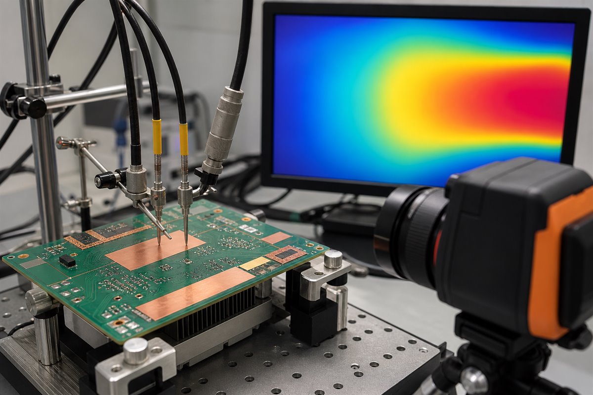
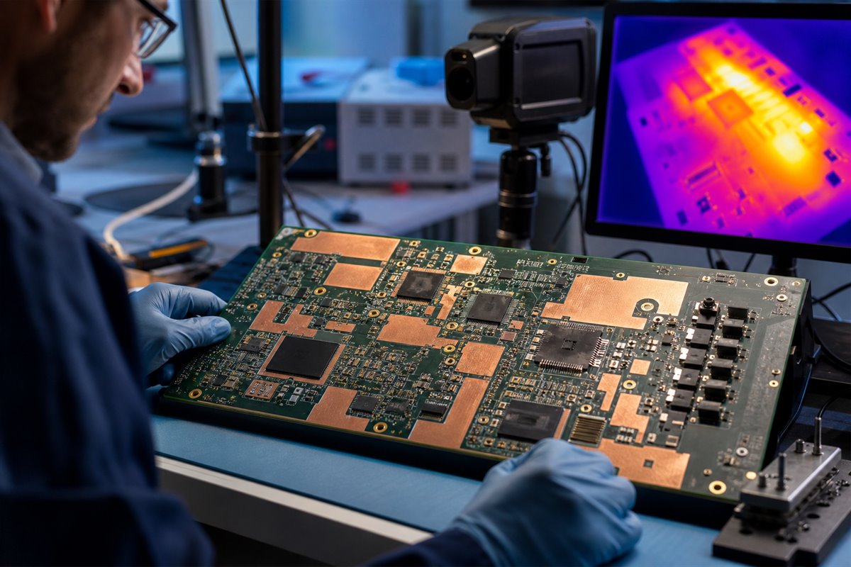
PCB copper heat-spreading measurement with probes and thermal imaging.

Copper Thermal Conductivity vs Aluminum for PCB Tradeoffs

At room temperature, copper conducts heat substantially better than aluminum: approximately 401 W/m·K versus about 237 W/m·K for pure aluminum. Copper can therefore move more heat through the same idealized cross-section, but conductivity alone does not select the best PCB construction.

Decision factorCopperAluminum-base option
Thermal conductivityAbout 401 W/m·KAbout 237 W/m·K
WeightHeavierLighter
PCB roleFoil, planes, and viasMetal-core base
Buyer checkCopper geometryDielectric and base

Choose the construction by the complete heat path, electrical isolation, weight, mechanical needs, achievable geometry, cost, and validation plan. A copper-heavy FR-4 board, an MCPCB, and a ceramic PCB solve different constraints; none should be selected from one W/m·K number alone.

PCB Project Example: Copper Thermal Conductivity in Heat-Spreading Checks

In one customer order, EBest Circuit reviewed a compact 47 × 34.5 mm, 12-layer FR-4 TG180 PCB built to IPC Class 3. The build combined blind vias from L1-L2 and L12-L11, buried vias from L2-L11, resin-plugged and plated-flat vias, a 2.0 mm finished thickness, and ENIG. Before production, the customer required the production stackup and CAM artwork for approval.

The thermal and manufacturing concern was not selecting another handbook conductivity value. The order data did not confirm the proposed 1 oz outer copper, while the residual copper area differed significantly among layers. Those details affect the real heat-spreading geometry, copper balance, and buildability even though bulk copper near room temperature remains about 401 W/m·K.

  • Outer-copper clarification: The customer had not confirmed 1 oz outer copper. EBest Circuit therefore kept it open in the EQ and production stackup instead of treating it as an approved input.
  • Via feasibility: The blind/buried sequence and resin-plugged, plated-flat vias required manufacturing review. The customer retained a ±2 mil via tolerance, so the released drawing and inspection basis had to preserve that decision.
  • Test-coupon confirmation: The COC mentioned a test coupon, but this order did not include impedance control. The customer confirmed that no coupon was needed, so the production documents were aligned with the agreed scope.
  • Copper balance decision: Because residual copper differed substantially by layer, engineering recommended a 1.0% bow-and-twist control. The customer did not accept the recommendation, so the decision was recorded and the production data remained customer-controlled.
  • Release gate: EBest Circuit issued the production stackup and CAM artwork for customer approval. Production could begin only after those documents were confirmed.

This order shows why copper thermal conductivity must be checked together with the actual stackup and released copper geometry. The credible supplier action was to surface unresolved data, preserve the customer's decisions, and gate production on approved manufacturing documents—not to claim that the 401 W/m·K material value alone guaranteed board temperature.

Copper thermal conductivity vs temperature
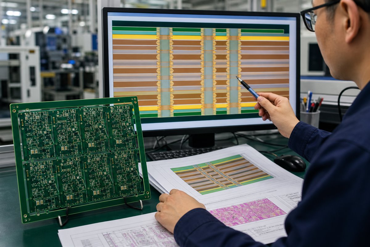
Production stackup and CAM review before releasing a 12-layer PCB order.

Copper Thermal Conductivity vs Temperature FAQs

Does copper thermal conductivity decrease as temperature increases?

Across typical room and elevated-temperature ranges, yes. Reference tables show a gradual decline as temperature rises. Cryogenic behavior is different and depends strongly on purity and RRR.

What copper thermal conductivity value should I use at room temperature?

About 400-401 W/m·K is a common bulk-copper reference near 20-27°C. State the source and do not treat it as the effective conductivity of the complete PCB.

Can I use one copper conductivity value for the full PCB temperature range?

Only for a rough model over a narrow range with adequate margin. For wide or critical ranges, use temperature-dependent data or defined temperature bands and correlate the model with testing.

Does thicker copper automatically solve a PCB hotspot?

No. Thickness can help, but plane area, bottlenecks, layer position, vias, dielectric interfaces, component attachment, and cooling boundary conditions also control the result.

What should I send for a PCB thermal and DFM review?

Send the controlled fabrication data, stackup, finished-copper requirements, drill data, BOM and placement data for assembly, expected operating range, heat-source information, thermal-interface assumptions, and the temperatures or test points that must be verified.

For a copper thermal conductivity vs temperature manufacturability review, contact EBest Circuit (Best Technology) at sales@bestpcbs.com with the controlled board package and operating assumptions. The review can then focus on the files, tolerances, heat-spreading features, and verification inputs that affect fabrication and assembly risk.

You may also like

Heat Transfer Coefficient of Copper: H Value Guide
Friday, June 26th, 2026

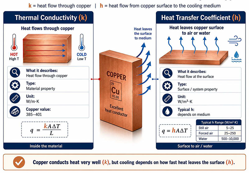
Heat transfer coefficient of copper is an important concept in thermal management, especially for heat sinks, copper core PCBs, heavy copper PCBs, copper inlay boards, PCB bus bars, heat pipes, cold plates, vapor chambers, and power electronics assemblies. Many people search for this term expecting one fixed value, just like the thermal conductivity of copper. In reality, these two terms are different. Copper has a high thermal conductivity, usually around 385–401 W/m·K for pure copper at room temperature, which describes how well heat travels through copper itself.

The heat transfer coefficient, often represented by h, describes how efficiently heat moves from a copper surface to a surrounding medium, such as air, water, oil, steam, or another contact surface. It is usually measured in W/m²·K and depends on cooling medium, airflow or liquid flow, surface area, surface finish, temperature difference, contact quality, and the full thermal path. For PCB, PCBA, heat sink, LED module assembly, EV charger, AI server power board, and industrial power electronics design, this distinction is important: copper can spread heat very well, but the heat still needs a real exit path.

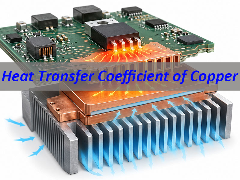
Heat Transfer Coefficient of Copper

What Is the Heat Transfer Coefficient of Copper?

The heat transfer coefficient of copper describes the rate at which heat moves between a copper surface and its surrounding environment. In heat transfer calculations, it is usually written as h.

The basic heat transfer equation is:

Q = h × A × ΔT

Where:

SymbolMeaning
QHeat transfer rate
hHeat transfer coefficient
AHeat transfer surface area
ΔTTemperature difference between the copper surface and the surrounding medium

This formula shows that heat transfer is not controlled by copper alone. Even if copper conducts heat quickly inside the material, the heat must still leave the copper surface.

For example, imagine the same copper plate used in three different conditions:

Copper ConditionHeat Transfer Result
Copper plate in still airHeat leaves slowly
Copper plate with fan airflowHeat leaves faster
Copper plate cooled by flowing waterHeat leaves much faster

The copper material is the same in all three cases. What changes is the cooling environment. That is why the heat transfer coefficient must always be discussed together with the actual working condition.

In simple terms:

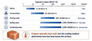
Copper helps heat spread. The surrounding medium decides how fast heat leaves.

Is the Heat Transfer Coefficient of Copper a Fixed Value?

No. The heat transfer coefficient of copper is not a fixed material value. This is the key point to understand before using it in thermal design. Copper thermal conductivity is a material property, while the heat transfer coefficient is a surface and system property.

Pure copper has high thermal conductivity because free electrons can carry thermal energy efficiently through its metallic structure. That is why copper is widely used in heat spreaders, heat pipes, cold plates, copper base PCBs, and high-current conductive parts. However, the h value depends on how heat leaves the copper surface, not only on the copper itself.

Copper ConditionHeat Transfer Result
Still airLow
Forced airflowHigher
Flowing waterMuch higher
Copper tubeFlow-dependent
Poor contactLimited
Good contactImproved

For example, a copper heat sink in still air may have limited cooling performance because air removes heat slowly. With stronger airflow, heat removal improves because moving air reduces the warm boundary layer near the copper surface. A copper cold plate with flowing water can transfer heat much more effectively than air cooling. A copper tube in a heat exchanger also depends on flow speed, tube diameter, wall thickness, and fouling.

So the better engineering question is not simply “What is the heat transfer coefficient of copper?” A more accurate question is: What is the heat transfer coefficient of this copper surface under this cooling condition?

This small change makes the answer more practical. It helps engineers evaluate copper parts based on real working conditions instead of treating copper as if it has one universal h value.

What Is the Unit of Heat Transfer Coefficient of Copper?

The standard unit of heat transfer coefficient is:

W/m²·K

It can also be written as:

W/(m²·K)

This means watts of heat transferred per square meter of surface area for every one kelvin of temperature difference.

This unit is different from the unit used for copper thermal conductivity.

ParameterSymbolUnitWhat It Describes
Thermal conductivity of copperkW/m·KHeat conduction through copper
Heat transfer coefficienthW/m²·KHeat exchange from surface to fluid
Overall heat transfer coefficientUW/m²·KTotal heat transfer through a full system

This distinction is useful because many users confuse these values.

For example, copper thermal conductivity may be around 401 W/m·K, but that does not mean the heat transfer coefficient of copper is 401 W/m²·K. The first value describes conduction through copper. The second type of value describes convection or surface heat exchange.

In PCB thermal design, both values matter. Copper thermal conductivity helps heat move through copper traces, planes, coins, or cores. The heat transfer coefficient affects how heat leaves the board through air, a heat sink, a housing, or a liquid cooling structure.

What Is the Difference Between Heat Transfer Coefficient and Thermal Conductivity of Copper?

Thermal conductivity and heat transfer coefficient are closely related, but they describe different stages of heat movement.

Thermal conductivity of copper answers this question:

How well does heat move through copper?

Heat transfer coefficient of copper answers this question:

How well does heat move from the copper surface to air, water, or another surrounding medium?

A practical example is a copper heat sink. The copper base spreads heat quickly from a hot component. This reduces local hot spots. But the heat still needs to move from the copper surface into the surrounding air. If airflow is weak, the copper heat sink may still run hot.

Another example is a copper core PCB. The copper core can spread heat from LEDs, MOSFETs, power ICs, or charging modules. But if the board does not have good contact with a housing or heat sink, the heat may remain inside the assembly.

So thermal design has two parts:

Heat Transfer StageMain Design Focus
Heat spreading inside copperCopper thickness, copper area, copper purity, copper path
Heat removal from copper surfaceAirflow, water flow, surface area, heat sink, housing contact

This is why high copper thermal conductivity alone does not guarantee low operating temperature. A good design must include a complete thermal path.

For PCBs, this means engineers should review copper thickness, copper plane area, via structure, dielectric thermal conductivity, component placement, soldering quality, surface finish, housing contact, and airflow path together.

Heat Transfer Coefficient of Copper

What Are Typical Heat Transfer Coefficient Values for Copper in Air and Water?

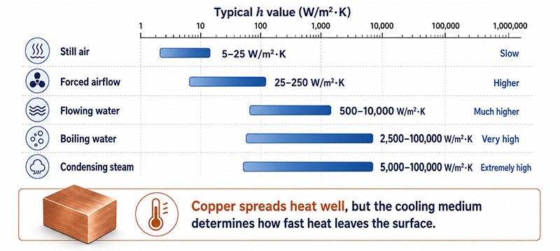
Copper does not have one fixed h value, but engineers often use typical ranges based on the cooling condition. These values are general reference ranges. Actual values should be verified by thermal simulation, testing, or project-specific calculation.

Cooling ConditionTypical Heat Transfer Coefficient Range
Natural convection in air5–25 W/m²·K
Forced convection in air25–250 W/m²·K
Water cooling500–10,000 W/m²·K
Boiling water or phase-change cooling2,500–100,000 W/m²·K
Condensing steam5,000–100,000 W/m²·K

These ranges explain why cooling method matters so much.

A copper plate in still air may not remove heat quickly, even though copper itself has excellent thermal conductivity. If a fan is added, the warm boundary layer near the copper surface becomes thinner, and heat leaves faster. If water is used as the cooling medium, heat removal can increase dramatically.

This is why high-power systems often use copper cold plates, copper tubes, heat pipes, or vapor chambers.

For PCB applications, air cooling may be enough for moderate power designs. For high-power LED modules, EV chargers, laser drivers, AI server power boards, or inverter modules, the design may require metal base PCBs, copper inlay, heavy copper, heat sinks, or liquid cooling assistance.

The key point is simple:

The copper part spreads heat. The cooling method removes heat. Both must work together.

Heat Transfer Coefficient of Copper

What Factors Affect the Heat Transfer Coefficient of Copper?

Several factors influence the heat transfer coefficient of copper in real applications. Understanding these factors helps engineers avoid thermal design mistakes.

Cooling Medium

  • Air, water, oil, and steam have different heat transfer behavior.
  • Air cooling is simple, clean, and low-cost, but its heat transfer coefficient is usually lower. Water cooling provides much stronger heat removal and is often used in high-power electronics, server cooling, EV charging, laser systems, and industrial power modules.
  • Oil cooling may be used in transformers or special power systems because it can offer insulation and stable thermal behavior. Steam condensation and boiling systems can provide very high heat transfer, but they require more complex design control.

Flow Speed

  • Flow speed has a major effect on h value. Still air creates a thick thermal boundary layer around the copper surface, which limits heat removal. Moving air reduces this layer and improves cooling.
  • The same logic applies to liquid cooling. Faster water flow usually improves heat transfer, but it also increases pressure drop and pump requirements. A practical design must balance thermal performance, noise, pressure loss, reliability, and cost.

Surface Area

  • A larger surface area allows more heat to leave. This is why heat sinks use fins. It is also why copper tubes, copper coils, and cold plates are shaped to increase contact area with air or liquid.
  • In PCB design, copper planes, thermal vias, exposed copper pads, copper coins, copper inlays, and metal bases can increase the useful heat spreading area.
  • However, more copper area only helps when the heat has a real exit path. A large copper plane inside a sealed product may spread heat, but the product can still overheat if the enclosure cannot release that heat.

Surface Condition

  • Copper surface condition also matters. Oxidation, roughness, plating, solder mask, contamination, and coating can change practical heat transfer.
  • For example, exposed copper may exchange heat differently from copper covered by solder mask. Nickel, tin, silver, ENIG, OSP, or other finishes may also influence surface contact, oxidation resistance, and assembly behavior.
  • In PCB production, surface finish is not chosen only for thermal reasons. It also affects solderability, shelf life, wire bonding, contact reliability, and cost.

Contact Resistance

  • When copper touches another material, the contact interface can become a thermal bottleneck. Air gaps, uneven pressure, poor soldering, weak thermal interface material, and rough surfaces can all increase contact resistance.
  • This is common in PCBA thermal issues. The copper may be thick enough, but the heat still cannot pass efficiently into the heat sink or metal housing.

Geometry

  • Copper geometry affects heat transfer. A copper plate, pipe, tube, rod, wire, coil, heat pipe, and copper coin all behave differently.
  • For example, the heat transfer coefficient of a copper tube depends on tube diameter, wall thickness, fluid velocity, internal surface condition, external cooling medium, and temperature difference. It cannot be judged only by the copper material.
  • In PCB design, geometry also matters. A short and wide copper path usually performs better than a long and narrow heat path. Thermal vias placed close to the heat source are usually more effective than vias placed far away.

How Does Copper Compare With Aluminum, Stainless Steel, and Other Metals?

Copper is one of the most practical metals for thermal design. Silver has higher thermal conductivity, but copper is more widely used because it offers a better balance of performance, cost, availability, machinability, and electrical conductivity.

MaterialApproximate Thermal ConductivityThermal Design Comment
Silver~429 W/m·KExcellent conductivity, but expensive
Copper~385–401 W/m·KStrong heat spreading and electrical conduction
Aluminum~205–237 W/m·KLightweight and cost-effective
Brass~80–120 W/m·KBetter mechanical/corrosion properties than pure copper, lower heat transfer
Stainless steel~14–16 W/m·KStrong and corrosion-resistant, but poor thermal conductor

Copper usually performs better than aluminum when fast heat spreading is required. This is useful when heat is concentrated in a small area, such as under a power IC, MOSFET, IGBT, LED chip, or laser diode.

Aluminum has lower thermal conductivity than copper, but it is lighter and more cost-effective. That is why aluminum heat sinks and aluminum PCBs are widely used in LED lighting, consumer electronics, automotive modules, and industrial control products.

Stainless steel is not usually selected for heat spreading. It is used when strength, corrosion resistance, or mechanical stability is more important than heat transfer.

The best material depends on the application:

Application NeedBetter Material Choice
Highest practical heat spreadingCopper
Lightweight heat sinkAluminum
High current and heat spreading togetherCopper
Low-cost LED thermal substrateAluminum PCB
Electrical insulation plus high thermal pathCeramic PCB
Corrosion-resistant structureStainless steel
Compact high-power moduleCopper core PCB or copper inlay PCB

For many real products, the best solution is not a single material. A thermal design may combine copper for heat spreading, aluminum for large fin area, ceramic for insulation, and thermal interface material for contact improvement.

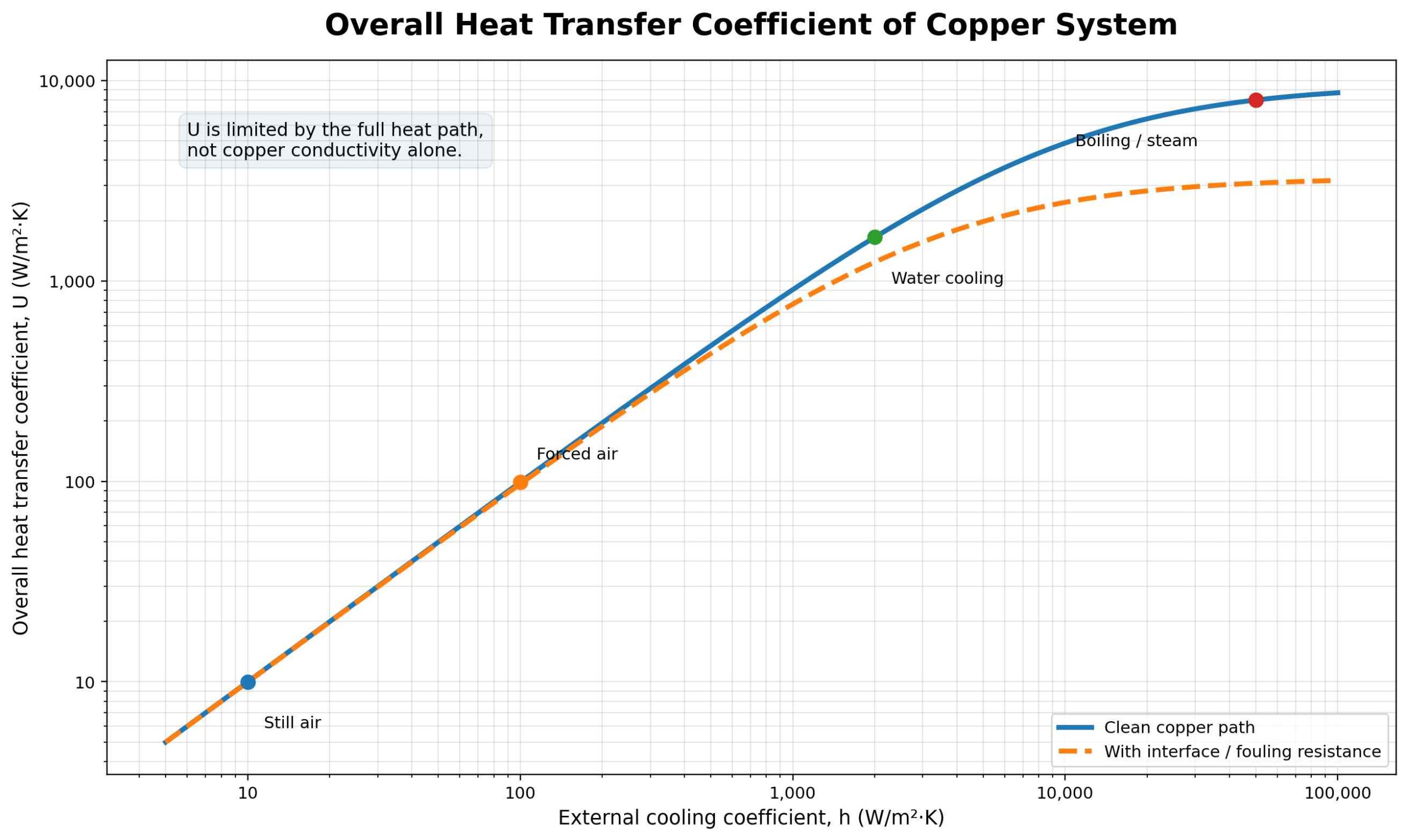
What Is the Overall Heat Transfer Coefficient of Copper?

The overall heat transfer coefficient, usually written as U, describes total heat transfer through a complete system. It includes all thermal resistance in the heat path.

This is different from the convective heat transfer coefficient h, which usually describes heat exchange at one surface.

For example, a copper tube heat exchanger may include:

  • Heat transfer from hot fluid to the inner copper wall
  • Heat conduction through the copper tube wall
  • Heat transfer from the outer copper surface to air or water
  • Fouling, oxidation, or coating resistance
  • Contact resistance at joints or interfaces

The U-value combines these effects. This makes it useful for heat exchangers, cold plates, copper tubes, liquid cooling systems, and multilayer thermal structures.

The same concept applies to PCB thermal design.

A copper core PCB thermal path may include:

Thermal Path SegmentPossible Thermal Issue
Component junction to packagePackage thermal resistance
Package to solder jointSolder voids or poor wetting
Solder joint to copper padPad size and copper connection
Copper pad to copper plane/coreCopper thickness and layout
Copper layer to dielectricDielectric thermal conductivity
Board to heat sink or housingContact resistance and flatness
Housing to airAirflow and surface area

This is why real thermal performance cannot be judged by copper alone. Copper is important, but the complete heat path decides the final temperature.

Heat Transfer Coefficient of Copper

Why Does the Heat Transfer Coefficient of Copper Matter in PCB, PCBA, and Heat Sink Design?

Copper is central to PCB manufacturing because it supports both electrical conduction and heat spreading. In high-power products, copper is not only a circuit material. It becomes part of the thermal management structure.

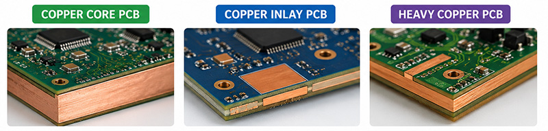
Heavy Copper PCB

  • Heavy copper PCB uses thicker copper to carry higher current and reduce resistance-related heating. It is often used in power supplies, EV chargers, battery systems, industrial controllers, motor drives, and automotive electronics.
  • Heavy copper also helps spread heat from power components. However, thicker copper does not automatically solve every thermal problem. Designers must also check trace width, copper balance, etching tolerance, soldering quality, thermal relief design, and the final heat exit path.
  • A common mistake is adding thick copper without improving airflow, heat sink contact, or board-to-housing conduction. In that case, heat spreads across the board but may not leave the product efficiently.

Copper Core PCB

Copper core PCB uses a copper base or copper core to move heat away from components. Compared with standard FR4, copper core structures offer much stronger heat spreading.

Copper core PCB is useful for:

  • High-power LED modules
  • Automotive lighting
  • MOSFET and IGBT boards
  • EV charging systems
  • Industrial power modules
  • Compact power conversion boards

The copper core spreads heat quickly, while the final temperature depends on dielectric thermal conductivity, copper thickness, contact area, heat sink design, and airflow.

Copper Inlay and Copper Coin PCB

  • Copper inlay and copper coin PCB structures place copper directly under high-heat components. This creates a shorter thermal path from the component to the heat dissipation structure.
  • These designs are useful when heat is concentrated in a small area, such as under power ICs, RF devices, LEDs, high-current terminals, or power modules.
  • For manufacturing, copper inlay and copper coin designs need careful DFM review. The supplier should check cavity tolerance, bonding reliability, copper thickness, lamination control, solderability, and board flatness.

Thermal Vias and Copper Planes

Thermal vias transfer heat from one PCB layer to another. Copper planes spread heat across a wider area. Together, they help reduce hot spots.

For better performance:

  • Place thermal vias close to the heat source
  • Use enough via quantity and copper plating thickness
  • Connect vias to large copper planes
  • Avoid isolated copper areas with no heat exit path
  • Consider solder wicking risk under components
  • Check whether vias should be filled, capped, or tented

Thermal vias are useful, but they are not magic. If the bottom side has no heat sink, no airflow, or no metal housing contact, the improvement may be limited.

Heat Sink and Housing Contact

  • A copper PCB or copper heat spreader needs a good contact path to the heat sink or enclosure. Poor contact pressure, uneven surfaces, air gaps, or weak thermal pads can reduce heat transfer.
  • For high-power PCBA, mechanical assembly matters as much as PCB material. Screw positions, flatness, thermal grease, gap pad compression, and enclosure material should be reviewed during design.

Common Design Mistakes

Many thermal problems are caused by layout and structure decisions made before production. Common mistakes include:

MistakeWhy It Causes Problems
Treating copper thermal conductivity as h valueLeads to wrong thermal assumptions
Adding copper without a heat exit pathHeat spreads but remains inside the product
Ignoring dielectric thermal resistanceMetal base performance becomes limited
Using too few thermal viasHeat cannot move efficiently between layers
Placing thermal vias too far from the heat sourceThermal path becomes longer
Covering key copper areas with solder maskSurface heat transfer and contact may be reduced
Poor heat sink contactContact resistance becomes the bottleneck
Ignoring solder voids under power partsJunction temperature may rise
Choosing heavy copper without DFM reviewEtching, spacing, soldering, and warpage risks increase

What Should Buyers Check Before Ordering Copper-Based Thermal PCBs?

For buyers and engineers, the right questions before ordering are important. A reliable PCB manufacturer should review not only board dimensions and copper thickness, but also the real thermal and electrical requirements.

Before ordering, check:

Item to CheckWhy It Matters
Copper thicknessAffects current capacity and heat spreading
Copper distributionAffects warpage, etching, and thermal balance
Base materialFR4, aluminum, copper, or ceramic changes the thermal path
Dielectric thermal conductivityCritical in metal core PCB
Thermal via designAffects heat transfer between layers
Surface finishAffects solderability, oxidation, and contact reliability
Solder mask openingAffects exposed copper and heat sink contact
Heat sink contact areaDetermines practical heat removal
Operating currentAffects Joule heating and trace temperature rise
Component power lossDetermines hot spot risk
Assembly methodAffects solder voids, contact, and reliability
Product environmentAirflow, enclosure, temperature, and humidity matter

This is where PCB manufacturing experience becomes important. A design may look correct in a schematic, but production details can affect thermal performance. DFM review helps identify these risks before fabrication and assembly.

At Best Technology, thermal PCB projects are usually reviewed from several angles: copper structure, material selection, stack-up, thermal path, manufacturability, assembly reliability, and application environment.

Heat Transfer Coefficient of Copper

FAQs About Heat Transfer Coefficient of Copper

Q1: What is the heat transfer coefficient of copper in W/m²·K?
There is no single universal value. Typical values may range from low natural air convection to very high liquid cooling or phase-change cooling values, depending on actual working conditions.

Q2: What is the heat transfer coefficient of copper to air?
Copper-to-air heat transfer is usually limited in still air. Forced airflow improves heat removal by reducing the warm boundary layer near the copper surface.

Q3: What is the heat transfer coefficient of copper and water?
Copper-to-water heat transfer is usually much stronger than copper-to-air heat transfer. This is why copper tubes, cold plates, and liquid cooling blocks are used in high-power systems.

Q4: Is copper better than aluminum for heat transfer?
Copper has higher thermal conductivity than aluminum, so it spreads heat faster. Aluminum is lighter and more cost-effective, so it is still widely used for heat sinks and LED aluminum PCBs.

Q5: Is copper better than stainless steel for thermal management?
Yes, when heat spreading is the main goal. Copper conducts heat much better than stainless steel. Stainless steel is usually chosen for strength, corrosion resistance, or structure.

Q6: What is the overall heat transfer coefficient of copper?
The overall heat transfer coefficient, or U-value, describes heat transfer through a complete system. It includes convection, conduction, surface condition, contact resistance, and other thermal barriers.

Q7: Why does the heat transfer coefficient of copper matter in PCB design?
It matters because copper spreads heat inside the PCB, but heat must still leave the board through air, heat sinks, metal housings, or liquid cooling. Good thermal PCB design must consider the complete heat path.

Q8: Can thicker copper always improve PCB heat dissipation?
Thicker copper can improve heat spreading and current capacity, but it does not always reduce final temperature. The board also needs a proper heat exit path, such as airflow, a heat sink, a metal base, or housing contact.

Q9: What PCB types are suitable for high thermal performance?
Common options include heavy copper PCB, copper core PCB, aluminum PCB, ceramic PCB, copper inlay PCB, and copper coin PCB. The best choice depends on power density, insulation requirement, current load, cost, and assembly structure.

To sum up, the heat transfer coefficient of copper is important in thermal design, but it should not be treated as a fixed copper material property. Copper has excellent thermal conductivity, which allows it to spread heat quickly. The heat transfer coefficient describes how efficiently heat leaves or enters the copper surface under specific cooling conditions.

For PCB and PCBA applications, copper plays a key role in heat spreading, current carrying, and product reliability. Heavy copper PCB, copper core PCB, copper inlay PCB, copper coin PCB, thermal vias, and copper planes can all improve thermal performance when they are designed with a complete heat path.

The best thermal design is not just about using more copper. It is about selecting the right copper structure, material stack-up, dielectric layer, surface finish, heat sink contact, airflow path, and assembly process.

At EBest Circuit (Best Technology), we support thermal management PCB and PCBA solutions, including copper core PCB, heavy copper PCB, aluminum PCB, ceramic PCB, copper inlay PCB, copper coin PCB, and full and partial turnkey PCB assembly. If your project involves LED modules, EV chargers, AI server power boards, industrial control boards, automotive PCBA, or high-current electronics, you can send your Gerber files, BOM, stack-up, copper thickness, and heat dissipation requirements to sales@bestpcbs.com for an engineering review and quotation.
You may also like

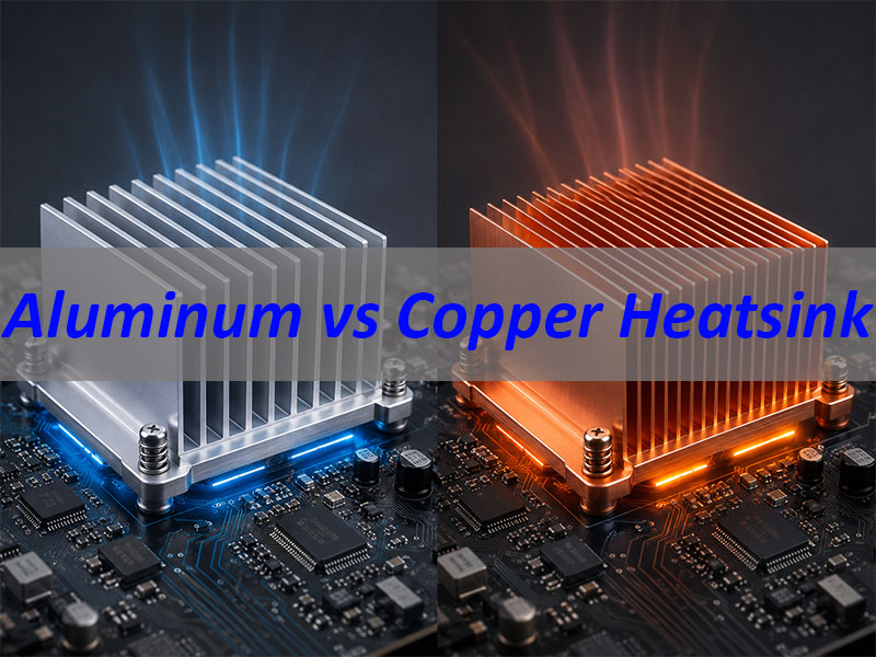
Aluminum vs Copper Heatsink: Which Is Better for PCB and PCBA Cooling?
Tuesday, June 23rd, 2026

When engineers compare an aluminum vs copper heatsink, they are usually looking for a better way to move heat away from electronic components. In PCB and PCBA projects, the heatsink is only one part of the thermal path. Heat must pass through solder joints, copper pads, PCB materials, thermal vias, metal cores, and finally to the heatsink, enclosure, or air. If this path is not well designed, even a high-performance heatsink may not fully solve overheating.

EBest Circuit (Best Technology) supports thermal management PCB and PCBA solutions, including aluminum PCB, copper core PCB, ceramic PCB, heavy copper PCB, and full turnkey PCB assembly. Since copper thermal conductivity is much higher than many common PCB materials, copper-based structures can help spread heat faster in high-power and high-current applications. Our engineering team can help review your PCB structure, copper thickness, material selection, component layout, and assembly requirements before production. If your project involves LED PCB, power electronics, automotive PCBA, industrial control boards, or high-current circuits, you can send your Gerber files, BOM, or thermal requirements to sales@bestpcbs.com for a practical engineering review.

Aluminum vs Copper Heatsink

Aluminum vs Copper Heatsink: What Is the Main Difference?

The main difference is simple: copper conducts heat better, while aluminum offers a better balance of weight, cost, and manufacturability.

Copper is useful when heat is concentrated in a small area. It can move heat away from power components faster, which helps reduce local hotspots.

Aluminum is lighter and easier to form into fins. Since heatsinks need surface area to release heat into air, aluminum is widely used for large cooling structures.

FactorCopperAluminum
Thermal conductivityHigherLower
WeightHeavyLight
CostHigherLower
Best useHotspots, compact high-power areasLarge fins, general cooling
PCB/PCBA roleHeat spreader, copper core, heavy copperAluminum PCB, MCPCB, external heatsink

In real products, many designs use both materials. A copper base spreads heat quickly, while aluminum fins provide larger cooling area with lower weight and cost.

Why Does Heatsink Material Matter in PCB and PCBA Thermal Design?

Heatsink material matters because it affects how quickly heat leaves critical components. But in PCB and PCBA design, it should not be selected alone.

A typical thermal path looks like this:

Component → solder joint → copper pad → PCB structure → heatsink → air or enclosure

If the PCB structure blocks heat transfer, the heatsink cannot work efficiently. For example, standard FR4 may not be enough for high-power LEDs, MOSFETs, IGBTs, or dense power modules.

Before choosing a heatsink, engineers should check:

  • Heat source position
  • Power density
  • Copper thickness
  • Thermal vias
  • Metal core material
  • Dielectric thermal conductivity
  • Component layout
  • Mounting pressure
  • Airflow and enclosure design

For low-power boards, FR4 with copper pours and thermal vias may be enough. For high-power products, aluminum PCB, copper core PCB, ceramic PCB, or heavy copper PCB may be more suitable.

Aluminum vs Copper Heatsink

Aluminum vs Copper Heatsink: Which Has Better Thermal Conductivity?

Copper has better thermal conductivity than aluminum.

Pure copper is usually around 385–401 W/m·K. Common aluminum materials are often around 205–237 W/m·K, depending on alloy grade and processing.

This means copper moves heat faster inside the material. When a component creates a small hotspot, copper can spread that heat more effectively.

However, heatsink performance also depends on surface area and airflow. Aluminum can be extruded into large fin structures, which helps release heat into the air at a lower cost and weight.

For PCB and PCBA cooling, the material choice often follows this logic:

NeedSuitable Option
Faster heat spreadingCopper core PCB, copper base, heavy copper
Lightweight coolingAluminum PCB, aluminum heatsink
High insulation and heat transferCeramic PCB
High current carryingHeavy copper PCB
General LED coolingAluminum PCB

Copper wins in conductivity. Aluminum often wins in cost, weight, and production practicality.

Why Are Most Heatsinks Made of Aluminum Instead of Copper?

Most heatsinks are made of aluminum because it is light, cost-effective, and easy to process.

Copper conducts heat better, but it is much heavier and more expensive. For the same size, copper is more than three times heavier than aluminum. In many PCBA products, that weight can create mechanical stress on the board or enclosure.

Aluminum can also be extruded into thin fins. This gives the heatsink more surface area, which is important for air cooling.

Aluminum is widely used in:

  • LED lighting modules
  • Power supply boards
  • Automotive electronics
  • Industrial control equipment
  • Communication devices
  • Consumer electronics
  • Aluminum PCB assemblies

Copper is usually used where its higher thermal conductivity brings clear value, such as copper bases, heat spreaders, copper cores, or high-power zones.

That is why aluminum is more common, but copper remains important in demanding thermal designs.

Do Copper Heatsinks Cool Faster Than Aluminum Heatsinks?

Copper can absorb and spread heat faster than aluminum. This is useful when heat is concentrated in a small area.

Typical examples include MOSFETs, IGBTs, power ICs, LED chips, processors, and high-current components. These parts can create local hotspots if heat is not moved away quickly.

But cooling speed is not decided by material alone. It also depends on:

  • Contact area
  • Thermal interface material
  • Mounting pressure
  • Fin design
  • Airflow
  • PCB copper area
  • Thermal via design
  • Soldering quality

A full copper heatsink may perform well, but it can be too heavy or expensive. In many cases, a copper base with aluminum fins is more practical.

At the PCB level, copper core PCB or heavy copper PCB can also help spread heat before it reaches the external heatsink. This can be more effective than simply adding a larger heatsink later.

Is Aluminum or Copper Better for PCB and PCBA Cooling?

For PCB and PCBA cooling, aluminum and copper solve different problems.

Aluminum is better when the product needs a lightweight, cost-controlled, and manufacturable cooling structure. It is widely used in LED PCB, power supply PCB, and many metal core PCB applications.

Copper is better when the design has high heat density, high current, or limited space. It is often used in copper core PCB, heavy copper PCB, copper inlay PCB, copper heat spreaders, or high-power thermal zones.

A practical selection rule is:

ApplicationCommon Thermal Choice
LED lightingAluminum PCB + aluminum heatsink
High-power LEDAluminum PCB, copper base, or ceramic PCB
Power supplyHeavy copper PCB + heatsink
Automotive power moduleCopper core PCB or ceramic PCB
Industrial control PCBAHeavy copper PCB or aluminum heatsink
High-current circuitHeavy copper, copper bus bar, copper core
Compact high-power moduleCopper spreader, ceramic PCB, copper core

The best material is not always the most expensive one. The right choice is the structure that keeps component temperature within a safe range while meeting cost, size, and reliability targets.

Aluminum vs Copper Heatsink

What Are the Weight and Cost Differences Between Aluminum and Copper Heatsinks?

Weight and cost are two major reasons aluminum is more common.

Copper has a density of about 8.96 g/cm³, while aluminum is about 2.70 g/cm³. For the same volume, copper is more than three times heavier.

This matters because many heatsinks are mounted directly on or near the PCBA. Extra weight can increase mechanical stress, screw requirements, vibration risk, shipping cost, and assembly difficulty.

Copper also costs more. It may require more careful machining and assembly control.

Aluminum is easier to process and better for large fin structures. It provides useful cooling area without making the product too heavy.

Still, the cheapest option is not always the best option. If poor thermal design causes overheating, unstable performance, LED lumen decay, or early failure, the total cost becomes much higher.

A cost-effective thermal design should match the PCB structure, heatsink material, and assembly process from the beginning.

When Should You Choose Copper-Based Thermal Solutions?

Choose copper-based thermal solutions when heat must move quickly from a small or high-power area.

Copper is suitable when the design has:

  • High heat density
  • High current
  • Limited board space
  • Compact structure
  • Strict temperature limits
  • Poor airflow
  • High reliability requirements

In PCB and PCBA manufacturing, copper-based solutions may include:

  • Copper core PCB
  • Heavy copper PCB
  • Copper inlay PCB
  • Copper coin PCB
  • Copper heat spreader
  • Copper base heatsink
  • Copper bus bar assembly

These options are common in power electronics, automotive modules, LED power boards, motor control, communication amplifiers, charging equipment, and other high-power products.

Copper should be used where its performance brings clear value. For many projects, copper near the heat source plus aluminum for larger dissipation area is a more balanced solution.

When Should You Choose Aluminum-Based Thermal Solutions?

Choose aluminum-based thermal solutions when the product needs good heat dissipation, lower weight, easier production, and better cost control.

Aluminum is suitable when the design has:

  • Moderate heat load
  • Larger cooling area
  • Cost-sensitive production
  • Weight-sensitive structure
  • LED lighting application
  • Good airflow or enclosure cooling
  • Mass production demand

In PCB and PCBA projects, aluminum is widely used in aluminum PCB, metal core PCB, LED PCB, power supply PCB, automotive lighting PCB, and industrial lighting modules.

Aluminum PCB is especially common in LED thermal management. It transfers heat from LED chips through the dielectric layer to the aluminum base, then to the heatsink or housing.

If the thermal requirement is not extreme, aluminum-based design is often the most practical choice. It offers a strong balance of performance, cost, weight, and manufacturability.

Why Choose EBest Circuit for PCB and PCBA Thermal Management Solutions?

Choosing between aluminum and copper heatsinks is only one part of thermal design. In many electronic products, the PCB and PCBA structure decide whether heat can move away from components efficiently.

EBest Circuit, also known as Best Technology, provides PCB and PCBA solutions for products that require stable heat dissipation. We support aluminum PCB, copper core PCB, ceramic PCB, heavy copper PCB, FR4 PCB, rigid-flex PCB, and turnkey PCB assembly.
We help customers select suitable thermal structures based on:

  • Power density
  • Current load
  • Heat source position
  • Product size
  • Working environment
  • Electrical insulation needs
  • Prototype or mass production quantity
  • Cost target

For LED lighting, automotive electronics, industrial control, power modules, communication equipment, medical electronics, and high-current PCBA projects, thermal performance is directly linked to reliability.

Our engineering team can help review Gerber files, stack-up, copper thickness, dielectric material, thermal vias, surface finish, BOM, component placement, and assembly requirements before production.
This helps identify thermal risks early, instead of discovering problems after PCBA testing or field use.

EBest Circuit supports both PCB fabrication and PCBA assembly, helping customers turn thermal design requirements into manufacturable products.

FAQs About Aluminum vs Copper Heatsink

1. Is copper better than aluminum for heatsinks?

Copper transfers heat faster, but aluminum is lighter, cheaper, and easier to form into large fin structures. Copper is better for high heat density. Aluminum is more practical for many general cooling designs.

2. Why are aluminum heatsinks more common than copper heatsinks?

Aluminum heatsinks are more common because they balance cooling performance, weight, cost, and manufacturability. Many products do not need full copper cooling.

3. Does copper dissipate heat better than aluminum?

Copper conducts heat better inside the material. But heat dissipation also depends on surface area, airflow, fin design, thermal interface material, and mounting quality.

4. Is a full copper heatsink worth it?

A full copper heatsink may be useful for compact, high-power products. For many designs, a copper base with aluminum fins gives a better balance.

5. Is aluminum or copper better for LED PCB cooling?

Aluminum PCB is commonly used for LED cooling because it is lightweight and cost-effective. Copper may be used for high-power LED modules that need faster heat spreading.

6. Is copper core PCB better than aluminum PCB?

Copper core PCB usually spreads heat better, but it costs more and is heavier. Aluminum PCB is suitable for many LED and power applications. Copper core PCB is better for higher heat density.

7. Can aluminum and copper be used together in one cooling design?

Yes. Many designs use copper near the heat source and aluminum for larger fin areas. This helps balance thermal performance, weight, and cost.

8. Can a heatsink solve all PCB overheating problems?

No. A heatsink works only when heat can reach it efficiently. If the PCB structure, solder pad, thermal vias, or dielectric material limit heat transfer, a larger heatsink may not fully solve the problem.

9. Which PCB material is best for thermal management?

There is no single best material for all products. Aluminum PCB suits many LED and power applications. Copper core PCB supports high heat density. Heavy copper PCB supports high current. Ceramic PCB is suitable for high thermal conductivity and insulation.
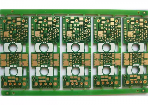
Choosing the right heatsink material is important, but reliable cooling depends on the full PCB and PCBA thermal path. If your project requires aluminum PCB, copper core PCB, ceramic PCB, heavy copper PCB, or turnkey PCBA with better heat dissipation, you can send your Gerber files, BOM, or thermal requirements to EBest Circuit at sales@bestpcbs.com for engineering review.

You may also like

PCB Thermal Conductivity Guide: Materials, Heat Dissipation & Thermal Design
Thursday, March 5th, 2026

If you work with electronic devices, you’ve probably heard of PCB thermal conductivity. But do you know what it really means? Or why it matters for your projects? This guide breaks down everything you need to know—from key materials to design tips

What Is PCB Thermal Conductivity?

PCB thermal conductivity refers to the ability of a printed circuit board material to transfer heat from one location to another. It is typically measured in W/m·K (Watts per meter-Kelvin).

A higher thermal conductivity value means heat travels more efficiently through the board. This helps prevent local hot spots and keeps electronic components operating within safe temperature limits.

Electronic components generate heat during operation. If the PCB cannot dissipate this heat effectively, several problems may occur:

  • Component overheating
  • Reduced electrical performance
  • Accelerated material aging
  • Solder joint fatigue
  • Unexpected system failure

Because of these risks, thermal performance is now a critical parameter in PCB design.
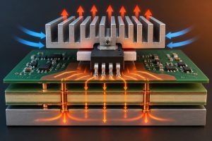
What Is PCB Thermal Conductivity?

What Is PCB Thermal Conductivity?

Why Thermal Conductivity is Important in PCB?

Thermal conductivity becomes especially important in systems such as:

  • LED lighting modules
  • automotive power electronics
  • RF communication equipment
  • industrial motor controllers
  • high-density computing hardware

In these systems, components like MOSFETs, power regulators, and RF amplifiers can generate significant heat during operation. A properly designed PCB spreads that heat efficiently across copper planes and into external cooling systems.
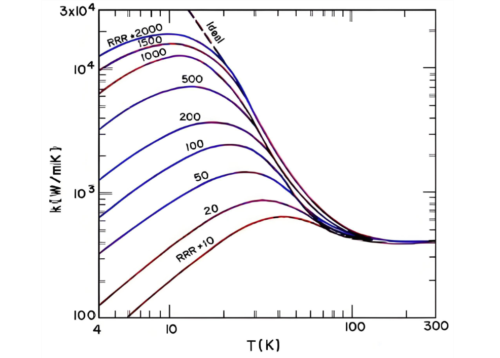
Thermal Conductivity of Common PCB Materials

Different PCB materials conduct heat at different rates. The base laminate, metal layers, and structural design all influence overall thermal performance.

The following table shows typical thermal conductivity values for common PCB materials.

PCB MaterialThermal Conductivity (W/m·K)Typical Applications
FR-4 Standard Laminate0.3 – 0.4Consumer electronics
High-Tg FR-40.4 – 0.6Industrial electronics
Aluminum PCB1 – 3LED lighting, power modules
Copper~385Heat spreading layer
Ceramic (Alumina)20 – 30RF modules, high-power circuits
Aluminum Nitride (AlN)140 – 180High-power semiconductor modules

Most standard PCBs use FR-4 epoxy glass laminate. While FR-4 is cost-effective and electrically stable, its thermal conductivity is relatively low. This is why designers often rely on copper planes and thermal vias to improve heat flow.

Which PCB Material Has the Highest Thermal Conductivity?

Among commonly used PCB materials, ceramic substrates offer the highest thermal conductivity.

Aluminum nitride (AlN) stands out because it combines high thermal conductivity with excellent electrical insulation. Its thermal conductivity can exceed 170 W/m·K, which is hundreds of times higher than standard FR-4. Despite its excellent thermal properties, AlN is significantly more expensive than FR-4. Manufacturing complexity is also higher.

Therefore, ceramic PCBs are usually reserved for applications that require extreme thermal performance, such as:

  • power semiconductor modules
  • high-frequency RF systems
  • aerospace electronics
  • high-power laser drivers

For most industrial products, aluminum PCB or optimized FR-4 stack-ups provide sufficient thermal performance at a more reasonable cost.

How Does Copper Thickness Affect PCB Thermal Conductivity?

Copper plays a major role in PCB heat spreading. Although the base laminate may have low thermal conductivity, copper traces and planes help move heat away from components. Copper has a thermal conductivity of approximately 385 W/m·K, which is extremely high compared with FR-4.

Increasing copper thickness improves thermal performance in several ways:

  1. Thicker copper spreads heat across a larger area.
  2. Reduced resistance helps decrease power loss.
  3. Heat moves more evenly through copper planes.

Typical PCB copper thickness values include:

Copper WeightThickness
1 oz~35 µm
2 oz~70 µm
3 oz~105 µm
4 oz~140 µm

Power electronics designs often use 2 oz or thicker copper. Heavy copper PCBs can reach 6 oz or even higher for extreme current applications. However, thicker copper also introduces design considerations:

  • trace spacing requirements increase
  • etching becomes more challenging
  • manufacturing cost rises

Therefore, engineers usually balance copper thickness with other thermal management methods such as thermal vias and heat sinks.

How Can You Improve PCB Thermal Conductivity in Design?

Even when using standard FR-4 materials, designers can significantly improve heat dissipation through thoughtful PCB layout and structure. Several design techniques are commonly used.

1. Use Larger Copper Planes

Copper planes distribute heat across the board surface, you can use large ground planes or power planes act as heat spreaders.

2. Add Thermal Vias

Thermal vias create vertical heat paths between layers. They allow heat to move from the component side to inner copper planes or heat sinks.

3. Select Metal Core PCB

Metal core PCBs use aluminum or copper substrates. These materials improve thermal conductivity and enable efficient heat transfer.

4. Optimize Component Placement

Components that generate significant heat should not be crowded together. Proper spacing helps air circulation and reduces temperature buildup.

5. Use Heat Sinks

External heat sinks remove heat from the PCB and release it into the surrounding environment.

What Is the Difference Between Thermal Conductivity and Thermal Resistance in PCB?

Thermal conductivity and thermal resistance are related but different concepts.

  • Thermal conductivity describes how well a material conducts heat.
  • Thermal resistance measures how difficult it is for heat to travel through a structure.

The relationship can be expressed as:

Thermal Resistance = Thickness / (Thermal Conductivity × Area)

In PCB design, this means:

  • thicker materials increase thermal resistance
  • higher conductivity materials reduce resistance
  • larger heat transfer areas improve cooling

Designers often calculate thermal resistance when evaluating cooling performance. A lower thermal resistance means heat can flow away from components more easily.

Where Are High Thermal Conductivity PCBs Used?

High thermal conductivity PCBs appear in many modern electronic systems. As power density increases, thermal design becomes more critical.

Common applications include:

  • LED lighting systems
  • automotive control modules
  • power converters and inverters
  • telecom base stations
  • RF amplifiers
  • industrial automation equipment

Similarly, power electronics used in electric vehicles require efficient thermal management. Heavy copper PCBs and thermal vias help maintain stable operating temperatures. In RF systems, excessive heat can affect signal stability, thermal control therefore supports both reliability and electrical performance.

Why Choose EBest as Your High Thermal Conductivity PCB Manufacturer?

At EBest Circuit (Best Technology), we focus on supporting engineers who require reliable PCB fabrication and assembly solutions for high-performance electronics. Our team has over 19 of experience in PCB and PCBA manufacturing. Our facilities operate in both China and Vietnam, allowing us to support global supply chains and flexible production requirements.

We work closely with customers during the early engineering stage. Our engineering team reviews design files and provides practical DFM feedback that helps improve manufacturability and thermal performance.

Our capabilities include:

  • multilayer PCB fabrication up to complex stack-ups
  • aluminum PCB and metal core PCB manufacturing
  • heavy copper PCB production
  • thermal via drilling and filling technologies
  • SMT and THT assembly services
  • component sourcing and turnkey PCBA

For PCB fabrication, thermal design consultation, or turnkey PCBA services, feel free to contact our team at sales@bestpcbs.com.

FAQ About PCB Thermal Conductivity

1. How can I improve PCB heat dissipation?

    Several design methods improve PCB heat dissipation. Common techniques include:

    • using thicker copper layers
    • adding thermal vias
    • increasing copper plane area
    • selecting aluminum PCB substrates
    • attaching external heat sinks

    2. What PCB material is best for thermal management?

    Ceramic materials such as aluminum nitride offer the highest thermal conductivity. However, aluminum PCBs provide an excellent balance between cost and performance. Many LED and power electronics systems use aluminum substrates. For general applications, optimized FR-4 with thermal vias can also deliver effective thermal management.

    3. Does thicker copper improve thermal conductivity?

    Yes. Thicker copper improves heat spreading across the board. Copper conducts heat extremely well. Increasing copper thickness creates larger thermal paths that help distribute heat more evenly.

    4. Is aluminum PCB better for heat dissipation?

    Yes. Aluminum PCBs provide significantly better heat dissipation than standard FR-4 boards.

    The aluminum base acts as a heat spreader and transfers heat quickly to external cooling systems.

    You may also like