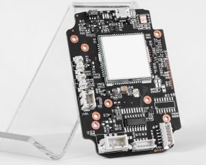
A capacitive touch PCB turns copper electrodes into buttons, sliders, wheels, touchpads or proximity sensors by measuring a change in capacitance. Reliable operation depends on the complete sensing stack, not only the copper pattern, so the PCB, overlay, adhesive, enclosure, controller settings and validation plan must be developed together.
EBest Circuit supports PCB design review, prototyping, component sourcing, fabrication and assembly for touch-control projects. Reviewing the electrode layout alongside the mechanical stack and test plan can uncover conflicts before they lead to enclosure rework or another prototype spin.
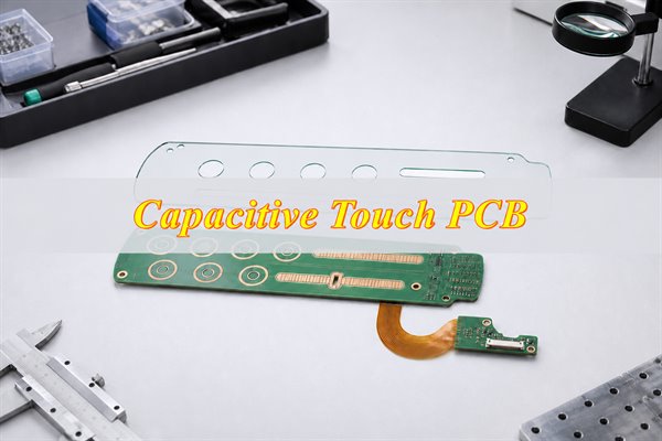
Are you worried about capacitive touch PCB performance after final assembly?
- Will the buttons still respond after the final glass or plastic overlay is installed?
- Could a charger, motor, display or wet surface cause false touches in the finished product?
- Will prototype tuning remain stable after adhesive, enclosure and production tolerances are introduced?
Drawing on more than 20 years of PCB and PCBA experience, EBest Circuit provides one-stop support by reviewing the sensor board, mechanical stack and production package as one release set.
- Mechanical-stack review: Align electrode geometry with the actual overlay, adhesive and enclosure so sensitivity is assessed in the finished construction.
- Layout and noise review: Check sensor routes, nearby switching nets, ground structures and shielding against the selected touch controller guidance.
- Prototype-to-production control: Freeze the approved PCB, overlay, firmware and test revision so later builds can be compared against the same baseline.
Ready to start your capacitive touch PCB project? Contact sales@bestpcbs.com to get a quote for your project.
What Is a Capacitive Touch PCB and When Should You Use It?
A capacitive touch board is appropriate when a product needs a sealed or low-wear interface and its enclosure can provide a controlled dielectric path between the user’s finger and the sensor electrode. Typical formats include buttons, sliders, wheels, touchpads and proximity inputs. A different input method may be safer behind a thick conductive cover, under uncontrolled liquid exposure or with gloves that the selected controller cannot reliably detect.
The sensor controller repeatedly measures the electrode’s baseline capacitance. A finger changes the electric field and produces a measurable delta. In self-capacitance sensing, one electrode is measured relative to its surroundings; in mutual-capacitance sensing, the controller measures coupling between transmit and receive electrodes. The controller architecture determines electrode topology, routing rules, scan method and tuning limits, so its reference design must be selected before the sensor layout is frozen.
- Use touch buttons: Choose individual electrodes when the interface needs discrete commands and clear activation zones.
- Use sliders or wheels: Choose segmented electrodes when firmware must estimate position across adjacent channels.
- Use proximity sensing: Choose a suitable controller and larger sensing field when detection must occur before physical contact.
Which Capacitive Touch PCB Structure Fits Your Product?
Select the sensor PCB construction by the mechanical path between the electrode and the touch surface. Rigid FR-4 suits supported flat panels, flex suits curved or tightly constrained interfaces, and rigid-flex connects fixed sensor and electronics zones through an integral flexible section. Whether the sensor is integrated with or separated from the main controller is a second architecture decision, not a PCB construction category.
Make this choice before layout freeze: construction changes the sensing distance, bend and registration controls, interconnection method and assembly checks.
| Sensor PCB Construction | Best Fit | Main Constraint | Verification Focus |
| Rigid FR-4 sensor PCB | Flat, mechanically supported control panels | Board-to-overlay spacing, panel flatness and enclosure support | Overlay stack, dimensional registration and assembled sensitivity |
| Flexible sensor circuit | Curved surfaces, thin interfaces or electrodes remote from the controller | Static or dynamic bend definition, coverlay and stiffener transition | Installed shape, bend condition, overlay stack and assembly variation |
| Rigid-flex sensor assembly | Fixed sensor and electronics zones requiring a permanent folded interconnect | Rigid-flex stack-up, transition geometry and installation sequence | Transition integrity, final folded geometry, overlay registration and assembled response |
Choose the PCB construction first, then choose the integration architecture. A separate sensor daughterboard can use rigid, flex or rigid-flex construction; select it when serviceability, panel replacement or separation from a noisy main board justifies an added connector or cable. Verify the resulting parasitic capacitance, ground-reference interaction, mechanical alignment and complete-system tuning.
If the sensor remains flat and the interconnect is short, rigid FR-4 normally provides simpler dimensional control. Use flex or rigid-flex when following a curved housing, reducing an air gap or relocating electronics provides enough benefit to justify additional bend, transition and assembly controls.
How Should a Capacitive Touch Button PCB Electrode Be Designed?
A touch electrode should cover the intended activation area without creating excessive baseline capacitance or overlap with adjacent sensors. Use the selected controller’s design guide as the geometry source, then verify the released pattern through the final overlay.
- Activation footprint: Map the visible icon and expected finger contact area to the electrode so the intended button produces a clear response without extending into an adjacent activation zone.
- Pattern topology: Use a solid or vendor-approved hatched region for a button and interleaved segments for a slider or wheel. Copying a button pad into a position sensor prevents the controller from resolving movement correctly.
- Trace exit: Route the sensor connection directly away from the pad, avoid wrapping it around neighboring electrodes and limit parallel exposure to switching nets. Treat the trace as part of the sensing capacitance, not as an ordinary digital connection.
- Channel consistency: Keep comparable buttons geometrically consistent unless the tuning plan explicitly compensates for different overlays, nearby metal or enclosure conditions. Unplanned differences can create unequal thresholds and user feel.
- Edge clearance: Check bezels, fasteners, displays, conductive coatings and chassis parts near every pad because they can redirect the field or raise baseline capacitance. Review the worst mechanical tolerance, not only nominal CAD alignment.
- Release evidence: Put electrodes, keep-outs, hatch patterns and sensor routes in controlled fabrication data. Approve the design only after the smallest and largest permitted pad/overlay conditions meet touch-delta, noise-margin and adjacent-channel criteria in the assembled enclosure.
How Do Overlay Material, Adhesive and Air Gaps Change Touch Sensitivity?
The overlay stack controls how strongly the finger couples to the electrode: greater distance and unintended air gaps usually weaken the touch signal, while dielectric material and consistent bonding determine how repeatable that coupling remains. Treat the complete stack as a sensor-design input before freezing the PCB layout.
- Material definition: Identify glass, polycarbonate, acrylic, printed film or coating by the released material specification because dielectric behavior and rigidity affect coupling differently.
- Total sensing distance: Control overlay, adhesive, paint and coating thickness together. A nominal cover dimension alone misses the layers that separate the finger from the electrode.
- Bonded interface: Specify adhesive type, bonded area, compression and permitted voids. An uncontrolled air gap can weaken or vary the signal even when the PCB and cover meet their individual dimensions.
- Mechanical features: Review molded ribs, local curvature, printed graphics and registration tolerance over each pad. Metal-filled ink or uneven geometry can change the field locally and make channels behave differently.
- Verification extremes: Use the controller vendor’s overlay guidance as the starting boundary, then test the thickest permitted stack, worst registration and relevant temperature/humidity conditions on representative assemblies.
How Should Capacitive Touch Sensor PCB Layout Control Noise and Parasitics?
Layout on a capacitive touch PCB must keep sensor capacitance stable and distinguishable from power, display, communication and switching noise. Short sensor routes, controlled separation and a controller-specific guard or shield strategy reduce coupling, but indiscriminate ground copper near or beneath the electrode can increase parasitic capacitance and reduce sensitivity.
- Sensor routing: Route each sensor trace directly to the controller, avoid long parallel exposure to clocks or switching nodes and treat its length as part of channel capacitance.
- Aggressor separation: Keep DC/DC converters, display clocks, high-current LED drivers and motor switching away from the sensor region where mechanics permit. If crossing is unavoidable, follow the controller guidance and avoid a long shared path.
- Ground placement: Select clearance, hatched ground, shield electrodes or driven shielding from controller documentation and measured SNR. A copied solid-ground rule can raise parasitic capacitance and reduce touch margin.
- Guard structures: Add a guard ring only when it provides the intended discharge or field boundary without consuming unacceptable channel margin; verify the result on the assembled stack.
- Power integrity: Apply the controller’s required decoupling and filtering, then measure channel noise with the actual charger, display and actuators operating.
- Layer and review record: Minimize vias, document layer changes and close the layout review with a channel map covering route length, nearby aggressors, shield/ground condition, mechanical stack and validation mode.
How Can a Capacitive Touch PCB Resist Water, EMI and False Touches?
False-touch resistance comes from combining electrode topology, shielding, clean power, controller algorithms and product-level validation. No single copper feature proves water or EMI immunity, and a design that works on a dry bench may fail when a wet film bridges neighboring electrodes or a switching load shifts the baseline.
- Liquid condition: Specify droplets, wet fingers, cleaning liquid, condensation and continuous flow separately. A water film can bridge electrodes, so dry-bench operation does not predict every exposure mode.
- Detection architecture: Evaluate mutual-capacitance sensing, shield electrodes, guard arrangements or firmware discrimination against the selected controller. Approve the option only when it preserves intended-touch margin as well as rejecting the defined liquid condition.
- Noise states: Operate chargers, displays, radios, relays, motors and converters during touch testing. Conducted or radiated interference can resemble a touch signal even when isolated channel data looks clean.
- False-outcome record: Log missed touches, false activations, neighboring-button activation and recovery after the disturbance. A pass/fail result without the failure type does not support tuning or root-cause analysis.
- ESD path: Review the overlay edge, enclosure, chassis and PCB protection path as one system. Protection must divert discharge energy from sensor/controller nodes without adding capacitance that destroys sensing margin.
What Must Be Frozen Before a Capacitive Touch PCB Prototype?
A useful prototype must freeze the sensor electronics, mechanical stack and firmware baseline together. If the PCB is tested with a temporary overlay or different adhesive, its behavior cannot reliably predict the finished product.
- Electronics identity: Freeze the controller, BOM, PCB stack-up, copper/solder-mask layers and firmware revision. A component or firmware change can shift baseline, filtering or channel behavior.
- Representative mechanics: Use the production-intent overlay, adhesive, printed graphics, enclosure features, connector/cable and nearby metal parts. Temporary covers or hand-held spacing do not represent the released field path.
- Raw-data access: Provide a debug method that exposes baseline, touch delta, noise or controller diagnostics. A binary button indication alone cannot show whether margin is shrinking.
- Sample variation: Include assemblies across permitted PCB, overlay, adhesive and registration tolerances rather than tuning one hand-selected unit.
- Controlled options: Populate alternate tuning footprints only when the evaluation plan defines the option, measured variable and selection criterion; uncontrolled variants make results ambiguous.
- Revision record: Bind every measurement to PCB, BOM, firmware, overlay and enclosure revisions plus power state and test mode so the result can be reproduced.
How Are Capacitive Touch PCBs Manufactured and Assembled?
Manufacturing must preserve the approved electrode geometry, dielectric stack, cleanliness and assembly registration while keeping the electronics build traceable. Bare-board electrical testing can confirm continuity and isolation, but only an assembled functional test can show whether the touch system responds correctly through the final overlay.
- Release controlled production data: Confirm Gerber or ODB++, NC drill, stack-up, electrode layer, solder-mask requirements, BOM, CPL, assembly drawings and revision identity. Misinterpreting the controlled copper source can create an electrode-geometry defect that survives basic continuity testing.
- Review manufacturability and panel handling: Check electrode clearances, flex transitions where applicable, fiducials, tooling, breakaway features and the effect of rails or tabs on the sensor area. Record the approved conditions in the production handoff; uncontrolled panel features can disturb the sensing field or damage sensitive geometry during handling.
- Fabricate and electrically inspect the bare board: Image, etch, laminate, drill, plate, apply solder mask and finish according to the released construction. Electrical test verifies opens and shorts; dimensional and visual inspection confirms the electrode artwork, registration and surface condition before assembly.
- Control components and substitutions: Match the touch controller, passives, connectors and protection components to the approved BOM. Any proposed substitute must be reviewed for pinout, capacitance, leakage, package, firmware support and supply-noise behavior so a mismatch does not create unstable sensing after release.
- Assemble the electronics: Print solder paste, place components and run the approved reflow process while protecting exposed or overlay-facing sensor surfaces from residues and mechanical damage. Inspection confirms polarity, placement and visible joints; hidden terminations require the inspection method defined for that package.
- Join the mechanical sensing stack: Align the PCB or flex electrode with the overlay, adhesive and enclosure using the approved drawing or fixture. Voids, contamination, skew and uneven compression create a functional failure risk and are recorded as defects because they can change coupling even when the electronics are correct.
- Program, tune and functionally verify: Load the controlled firmware, apply the intended calibration procedure and test every input through the assembled overlay. Release evidence should identify unit, hardware revision, firmware, test conditions and pass/fail criteria so any false or missed detection failure blocks release.
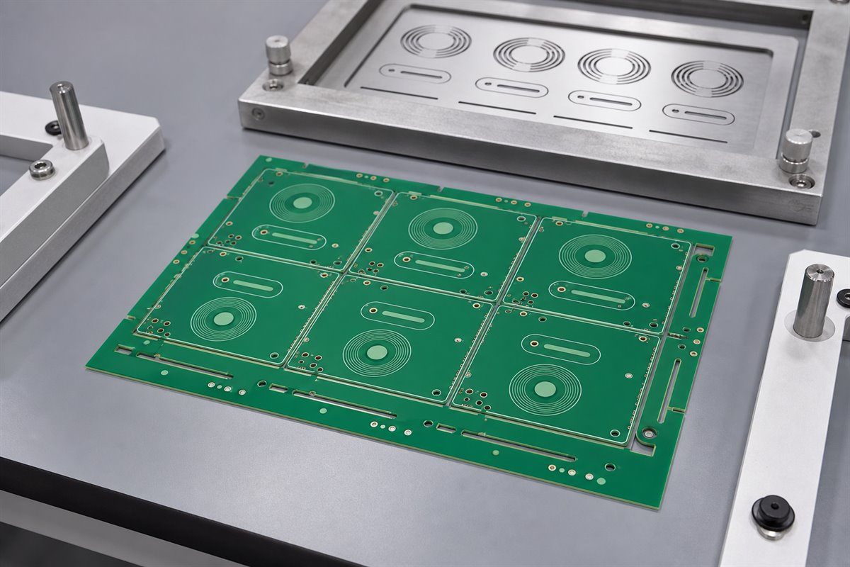
This sequence separates four different proofs: artwork and construction inspection, bare-board electrical test, assembly inspection and functional touch verification. A purchasing specification should name which records are required instead of treating one inspection result as proof of the entire system.
How Should Capacitive Touch PCB Testing and Tuning Be Planned?
Testing should measure touch separation from noise across real mechanical, electrical and environmental variation. A finger demonstration on one open board is only a bring-up check; production release needs controlled samples, repeatable stimuli, recorded controller data and acceptance criteria linked to the intended product.
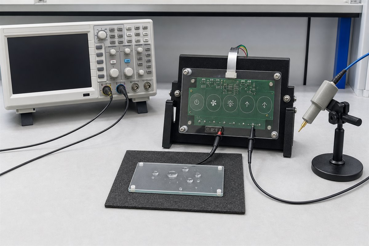
- Baseline and touch margin: Record baseline capacitance or the controller’s equivalent raw value, touch delta, noise and neighboring-channel response. Set thresholds only after the worst measured separation is understood.
- Engineering tuning: Adjust thresholds, filters, scan timing and shield settings within the controller’s supported range, then retain the raw before/after data and firmware identity.
- Mechanical variation: Repeat measurements across permitted overlay, adhesive and registration tolerances. A tuning value derived from one nominal assembly cannot prove production margin.
- System disturbance: Exercise charger, display, radio, motor and converter states on the complete product and record both false and missed detections by channel.
- Environmental conditions: Apply specified dry-finger, glove, liquid, temperature or humidity conditions with stabilization and recovery criteria defined in the test plan.
- Production functional test: Use a controlled fixture or actuation method to check every channel and log unit identity, hardware revision, firmware, test condition and result.
Release only when the recorded sample range, assembled stack, test configuration, acceptance thresholds and exceptions provide a reproducible baseline for later lots or field-return comparison.
Where Are Capacitive Touch PCBs Used in Medical, Aerospace and Industrial Products?
Capacitive touch interfaces can serve sealed control surfaces in medical, aerospace and industrial products, but each application changes the failure consequences and verification burden. The examples below are design-review scenarios, not claims about completed EBest Circuit customer programs.
- Medical control-panel example: A device interface may need cleaning-fluid tolerance, clear feedback and controlled behavior with approved gloves. Review the overlay chemistry, liquid exposure, alarm-related command risk, usability validation and the quality-system requirements assigned to that product.
- Aerospace interface example: A cabin or equipment-panel control may face vibration, temperature variation, ESD and electromagnetic disturbances. Confirm whether touch input is suitable for the command criticality and specify tactile, visual or audible feedback plus a safe response to ambiguous activation.
- Industrial HMI example: A machine panel may encounter wet gloves, oil, metal enclosures, inverters and motor noise. Separate touch electronics from switching nodes where practical, review grounding at system level and test during the machine’s highest-disturbance operating states.
Certifications held by a supplier do not automatically certify a board or finished device. The order must identify its applicable quality plan, documentation, inspection, traceability and product-level compliance responsibilities before production release.
Why Choose EBest Circuit for Capacitive Touch PCB Projects?
EBest Circuit can support the connected tasks that move a touch-control design from released files to verified assemblies. PCB review, prototyping, sourcing, fabrication and assembly stay tied to the same product definition and revision.
- Design review: Identify electrode, routing and mechanical-stack questions before they become prototype respins.
- Prototype support: Build controlled samples that let the project compare tuning changes against known hardware revisions.
- Rigid and flex options: Align the sensor construction with flat, curved or space-constrained product mechanics to avoid unnecessary interconnects.
- Component sourcing: Keep touch controllers, protection parts and approved alternates aligned with the released BOM.
- PCB assembly: Reduce handoff gaps between bare-board fabrication, component placement and functional test preparation.
- Production continuity: Keep approved files and revision identity controlled when a validated prototype moves toward repeat builds.
What Files Are Needed for a Capacitive Touch PCB Quote?
A useful quotation needs both standard PCB/PCBA production data and the mechanical sensing-stack information that changes touch behavior. Sending only a schematic or board image leaves electrode construction, assembly scope and test responsibility unresolved.
- PCB fabrication: Gerber or ODB++, NC drill, stack-up, board outline, copper requirements, surface finish and fabrication notes.
- Assembly: BOM with manufacturer part numbers, CPL/pick-and-place file, assembly drawings, approved substitutions and programming instructions.
- Touch mechanics: Electrode drawing, overlay material/thickness/tolerance, adhesive stack, printed coating and enclosure or bezel drawing.
- Functional context: Touch-controller part number, firmware/tuning ownership, input types, expected gloves or liquid exposure and interface feedback.
- Verification: Required inspections, electrical test, functional test method, acceptance criteria, records and traceability level.
- Commercial scope: Prototype and production quantities, delivery destination, packaging needs and controlled revision.
When functional test development is requested, also provide a known-good unit or an approved behavior specification. The test team then has a measurable release target instead of an unspecified instruction to “test the touch buttons.”
FAQs About Capacitive Touch PCB Design and Manufacturing
Q1: Can a capacitive touch electrode be placed on an inner PCB layer?
A1: It may be possible when the added dielectric distance still leaves verified sensing margin. Use the controller guidance to evaluate the layer stack, copper above the pad and overlay distance, then compare raw channel data with the outer-layer option before release.
Q2: Should solder mask be opened over a touch electrode?
A2: Usually not when the electrode senses through a cover and does not need electrical contact. Keeping the mask can protect the copper, but the released mask thickness and any opening must match the tested construction instead of being changed as a cosmetic fabrication decision.
Q3: Can an LED backlight be placed behind a capacitive touch button?
A3: Yes, if the optical opening, LED drive and electrode pattern are evaluated together. The cutout can reduce sensing area, while LED switching can inject noise. Measure the channel with the backlight off, dimmed and at maximum intended activity.
Q4: Can sensor channels pass through a connector or cable?
A4: They can, but the interconnect becomes part of the capacitive and noise environment. Review length, adjacent conductors, shielding, connector contamination and motion, then tune and verify the complete connected assembly rather than qualifying only the local sensor board.
Q5: How should unused touch-controller channels be handled?
A5: Follow the selected controller’s datasheet instead of applying a universal tie-off rule. An unused input may require disabling, grounding or another defined state. Record the firmware and hardware treatment so production inspection can distinguish an intentional condition from an assembly fault.
Q6: Should production functional testing also tune every unit?
A6: Only when the controller and released process explicitly use controlled per-unit calibration. Otherwise, production should apply the approved configuration and verify acceptance limits. Uncontrolled unit-by-unit threshold adjustment can hide mechanical or assembly variation instead of detecting it.
Q7: Can protective shipping film affect final touch inspection?
A7: Yes, when the film adds distance, traps moisture or differs from the intended user surface. Specify whether testing occurs with the film installed or removed, and do not mix both conditions in one acceptance dataset without separate limits.
Q8: Is ENIG required for capacitive touch electrodes?
A8: Not when the electrode remains under solder mask or an overlay and does not need exposed contact. Select the surface finish for the complete PCB’s solderability, exposed-contact and storage requirements, then verify that the released mask openings match the sensor construction.
Q9: Can panel rails or breakaway tabs affect a touch electrode?
A9: Yes, when temporary copper, tooling or mechanical stress sits close to the sensing area. Review the panelized geometry as well as the finished outline, control tab location and depaneling stress, and confirm that post-depanel channel data matches the approved sample.
Q10: Who should own capacitive touch firmware settings?
A10: Assign one owner for thresholds, filters, calibration and released firmware identity. The PCB supplier can build and test against an approved configuration, but hardware acceptance becomes ambiguous when engineering, assembly and production use different unrecorded settings.
Conclusion
A capacitive touch interface is ready for release only when every controlled input matches the tested build. The electrode, overlay, adhesive, enclosure, routing, controller settings and validation records must carry the same revision identity. Acceptance should come from stable operation through the intended mechanical stack and disturbance conditions, not an open-bench finger demonstration.
EBest Circuit provides PCB design review, prototyping, fabrication, component sourcing and assembly support for capacitive touch projects. For a free DFM review and quotation, send your PCB files, BOM, CPL, overlay/enclosure drawings, controller information, test requirements and quantities to sales@bestpcbs.com.