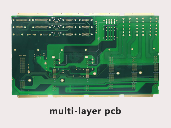
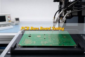
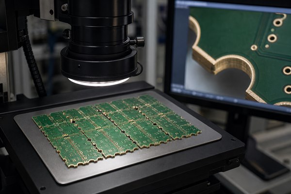
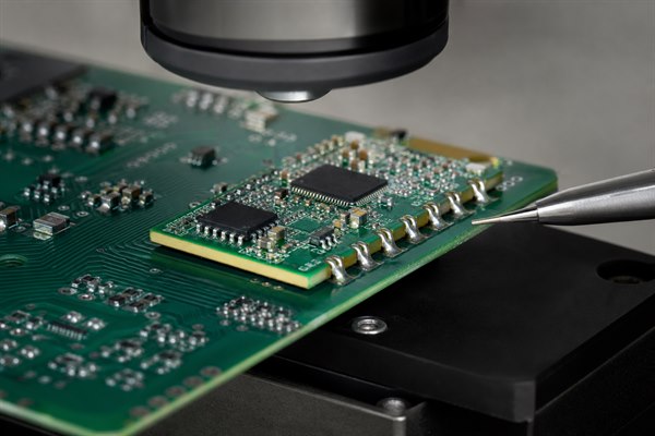
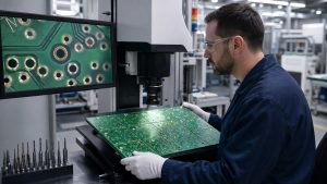
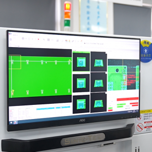
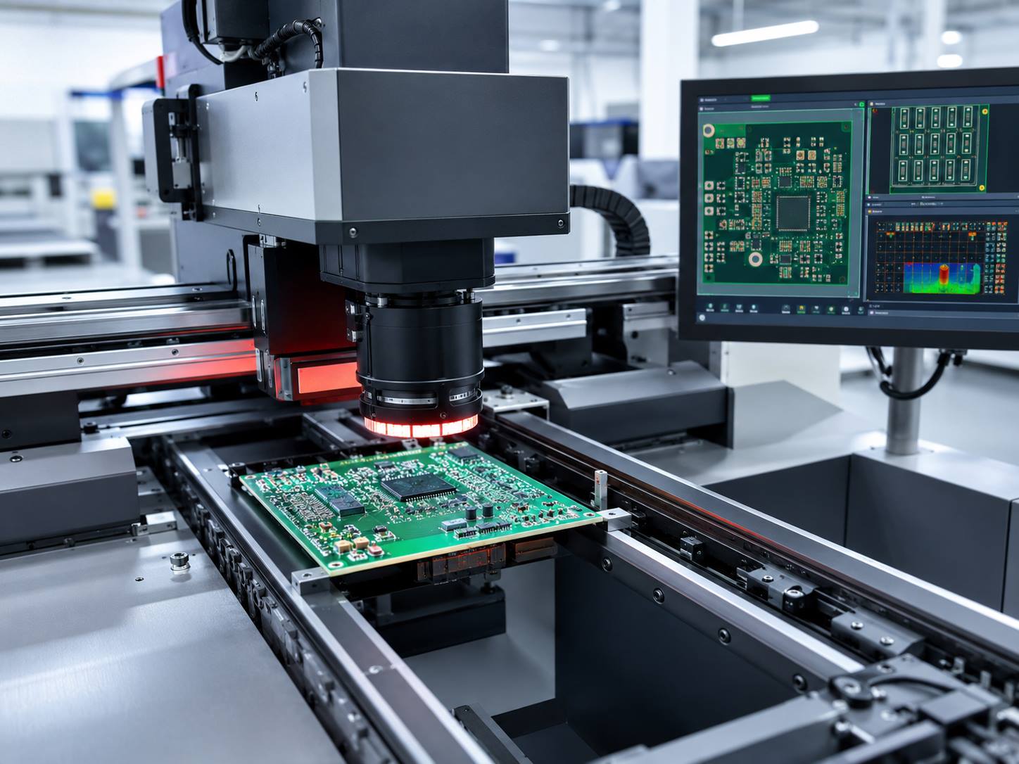
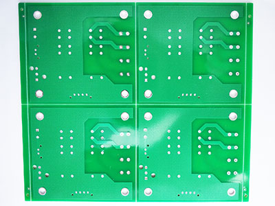
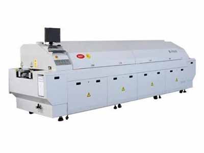
AOI in PCB manufacturing means automated optical inspection: a camera-based inspection process used to find visible defects on bare PCBs or assembled PCBAs before they move to the next production step. It helps manufacturers catch issues such as missing components, wrong polarity, solder defects, bridging, insufficient solder, misalignment, surface damage, and certain pattern defects, but it does not replace every electrical, X-ray, or functional test.
This guide explains where AOI fits in PCB and PCBA quality control, what it can detect, what it cannot prove, and what buyers should ask before sending an RFQ for production or assembly.
AOI in PCB Manufacturing at a Glance
AOI is a fast visual inspection method that compares PCB or PCBA images against programmed inspection rules. It is useful because many defects are visible before the board reaches final testing.
Inspection point
AOI can help check
AOI cannot fully replace
Bare PCB
Pattern defects, solder mask issues, surface contamination, open or short risk clues
Full electrical testing and final acceptance criteria
Hidden solder joint X-ray or powered functional testing
Final PCBA
Visible assembly defects and workmanship consistency
Firmware, load, signal, thermal, or application-specific tests
Where AOI Fits in the PCB Production Flow
AOI is usually placed after a manufacturing or assembly step where visible defects should be caught before more value is added to the board. In SMT assembly, AOI is commonly used after solder paste and reflow-related steps depending on the process plan. In bare PCB manufacturing, optical inspection can help flag pattern or surface issues before later processing.
For buyers, the important question is not simply whether AOI exists. Ask where it is used, which defect types are checked, and whether findings are reviewed by trained staff before boards are released.
What AOI Can Detect on PCBAs
AOI is strongest at detecting visible component and soldering problems on assembled boards. It is especially useful when there are many SMT parts and manual visual inspection would be slow, inconsistent, or easy to miss.
Missing, shifted, skewed, or rotated components
Wrong polarity on LEDs, diodes, ICs, or capacitors when markings are visible
Solder bridges and visible insufficient solder
Tombstoning, lifted leads, and package placement issues
Surface contamination or visible damage
For assembled projects, AOI should connect with the broader PCBA service workflow rather than standing alone as a checkbox.
What AOI Can Detect on Bare PCBs
For bare boards, optical inspection can help identify visible pattern, solder mask, silkscreen, and surface issues before shipment or assembly. It may flag scratches, contamination, missing features, copper pattern problems, solder mask misregistration, or visual abnormalities that need review.
AOI is only one layer of control. Bare-board electrical testing, process control, material verification, and final inspection still matter, especially for boards with fine features, controlled impedance, high current, or special materials.
AOI vs SPI, X-Ray and Functional Testing
AOI checks visible features, SPI checks solder paste, X-ray checks hidden structures, and functional testing checks whether the circuit works under defined conditions. These tests answer different questions.
Method
Best for
Typical limit
SPI
Solder paste volume and print quality before placement
Does not prove final component function
AOI
Visible placement and solder defects
Cannot see every hidden joint or prove circuit function
X-ray
BGA, QFN, hidden solder joints, voiding review
Not usually needed for every simple board
Functional test
Power, signal, firmware, application behavior
Requires buyer-defined test plan or fixture
AOI Limits Buyers Should Understand
AOI reduces visual defect risk, but it does not guarantee that every board will pass electrical or application testing. It depends on the inspection program, image quality, board design, component markings, operator review, and whether the defect is visible to the camera.
Hidden BGA solder joints, internal layer issues, marginal electrical behavior, thermal performance, firmware problems, and intermittent failures may require other test methods. Buyers should define the risk level and ask which inspection combination is appropriate.
How AOI Supports DFM and Process Feedback
AOI findings can feed back into DFM and process improvement when recurring defects point to pad design, stencil, placement, soldering, or component issues. If the same defect appears repeatedly, the supplier should not only sort boards. They should investigate the cause.
Examples include solder bridging caused by pad spacing, tombstoning caused by land pattern imbalance, weak polarity markings, or recurring placement offsets. This is why quality control should connect to engineering review before repeated production.
AOI for SMT, Through-Hole and Mixed Assembly
AOI is most common in SMT inspection, but mixed assemblies still need a planned inspection approach. Through-hole parts, connectors, large components, and hand-soldered features may need visual inspection, selective process checks, or functional testing in addition to AOI.
For through-hole-heavy projects, review the assembly route and inspection plan before quoting. The through-hole assembly page can be useful when a project combines SMT and mechanical-strength components.
What Buyers Should Ask About AOI Before RFQ
Buyers should ask what AOI checks, when it is used, what defect criteria apply, and what other tests are needed for the product. A supplier that only says “AOI included” has not given enough information for a high-risk board.
At which production stages is AOI used?
Which defect types are programmed for this board?
Are AOI findings reviewed before release?
Does this board need X-ray because of BGA, QFN, or hidden joints?
Does the buyer need to provide firmware, fixtures, or functional test requirements?
Cost and Lead-Time Impact of AOI
AOI can add inspection steps, but it often reduces downstream rework risk for assemblies with many components or visible soldering risk. The impact depends on board complexity, production volume, inspection program setup, and whether other tests are also required.
For quote planning, include test and inspection expectations early instead of adding them after the price is approved. The custom PCB cost guide can help buyers understand why inspection and testing should be treated as cost factors, not afterthoughts.
RFQ Checklist for AOI and PCB Quality Control
An RFQ should define the board files, assembly files, component risk, and inspection expectations clearly enough for the supplier to recommend the right quality plan.
Gerber or ODB++ files and drill data
BOM and CPL if assembly is required
Assembly drawing, polarity notes, and test point requirements
Package types such as BGA, QFN, fine-pitch ICs, connectors, or LEDs
Required inspection: AOI, X-ray, electrical testing, programming, or functional testing
Acceptance criteria and known product risks
Frequently Asked Questions
What does AOI mean in PCB manufacturing?
AOI means automated optical inspection. It uses cameras and programmed inspection rules to identify visible defects on bare PCBs or assembled PCBAs.
Can AOI replace functional testing?
No. AOI checks visible defects. Functional testing checks whether the circuit works under defined electrical or application conditions. Many projects need both.
Is AOI needed for every PCB assembly?
Not always. It is most valuable when there are many SMT components, fine-pitch packages, polarity-sensitive parts, or higher reliability requirements. Simple boards may need a lighter inspection plan.
Does AOI find BGA solder defects?
AOI can inspect visible features around BGA placement, but hidden solder joints usually require X-ray or another suitable inspection method.
What should I send if I need AOI and testing?
Send Gerber or ODB++ files, BOM, CPL, assembly drawing, package notes, test requirements, firmware or fixture needs, quantity, and acceptance criteria.
Send PCB Inspection and Assembly Requirements
If your PCB or PCBA project needs AOI, X-ray, functional testing, or a defined quality-control plan, send your Gerber or ODB++ files, BOM, CPL, assembly drawing, package details, quantity, and test requirements to the Best Technology / bestpcbs engineering team at sales@bestpcbs.com. The team can review which inspection steps fit the board design, assembly risk, and shipment requirements before production starts.
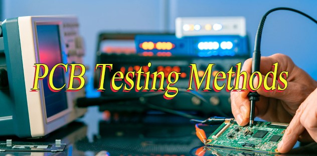
To test a PCB board, start with visual inspection, then check continuity, resistance, shorts, power rails, component orientation, signal behavior and functional output. A good PCB test process does not rely on one tool only. It combines simple inspection, multimeter checks, controlled power-up, and fixture or system-level testing when the board is part of a product.
This guide explains how to test a PCB board before repair, assembly validation or production release. It is written for engineers, buyers and quality teams who need a practical checklist without turning the article into a lab manual.
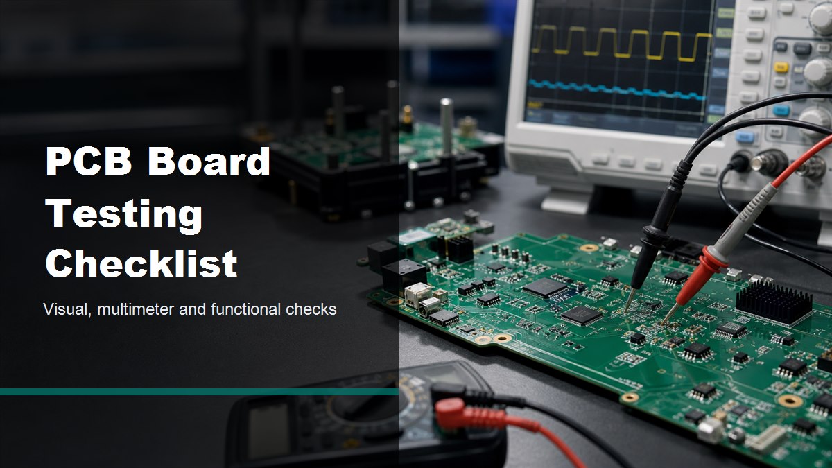
PCB board testing should combine visual inspection, multimeter checks and controlled functional testing.
What Should You Check First on a PCB Board?
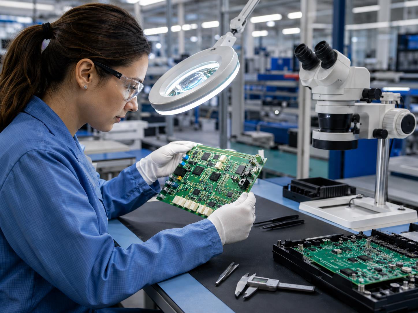
First, check the board visually before applying power. Many PCB failures can be found before using a meter, especially solder bridges, burned areas, cracked components, lifted pads, reversed parts and contamination.
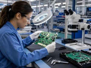
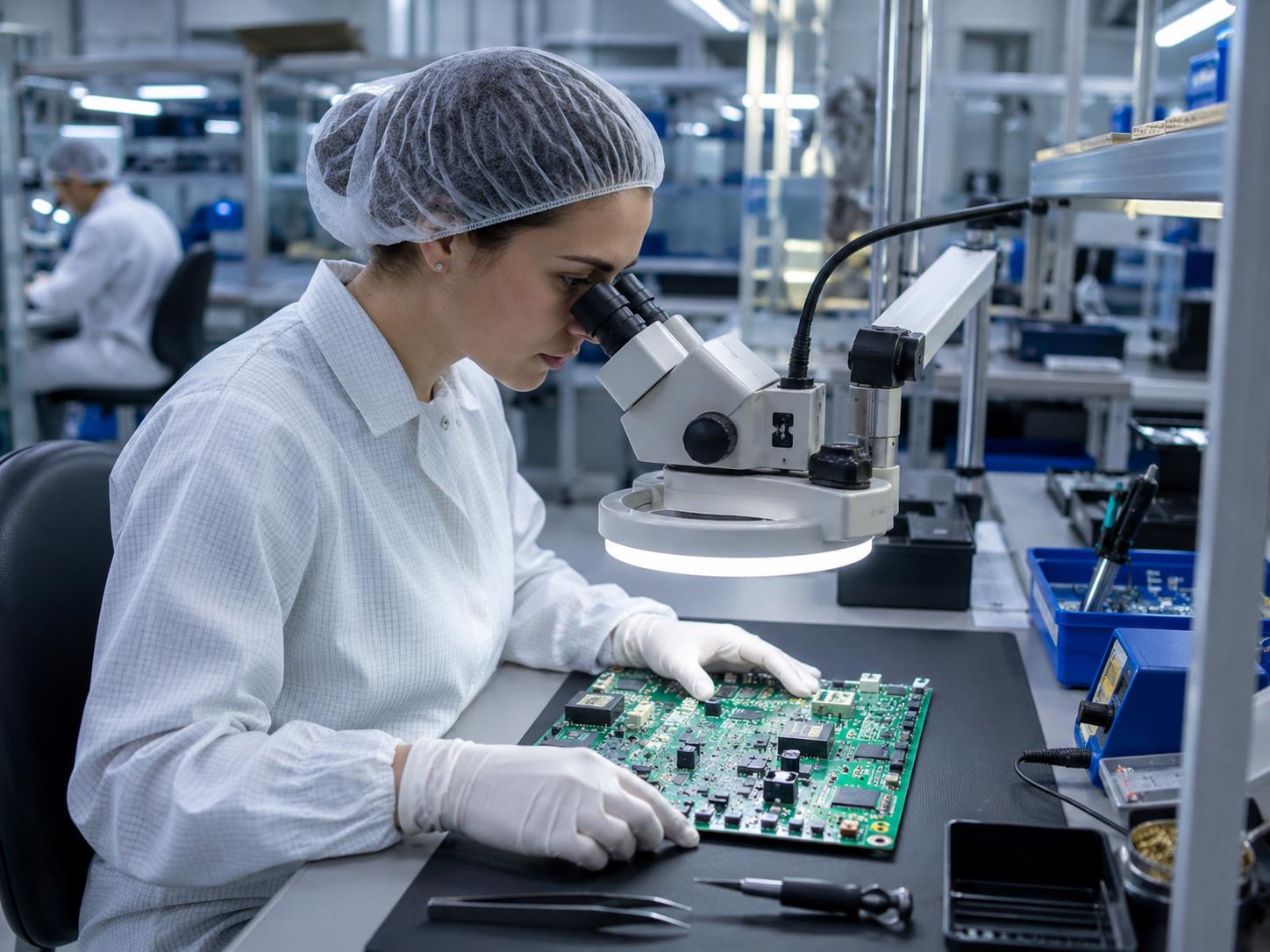
Look at the PCB under bright light or a microscope if the board has fine-pitch ICs, small passives, BGA packages or dense routing. For a new board, compare the actual assembly against the BOM, silkscreen and assembly drawing. For a failed board, look for local heat damage, darkened solder mask, bulged capacitors, broken connectors and corrosion around exposed copper.
Do not power a board that already shows a visible short, carbonized area, reversed electrolytic capacitor or damaged regulator. Those faults can turn a small repair into a larger failure.
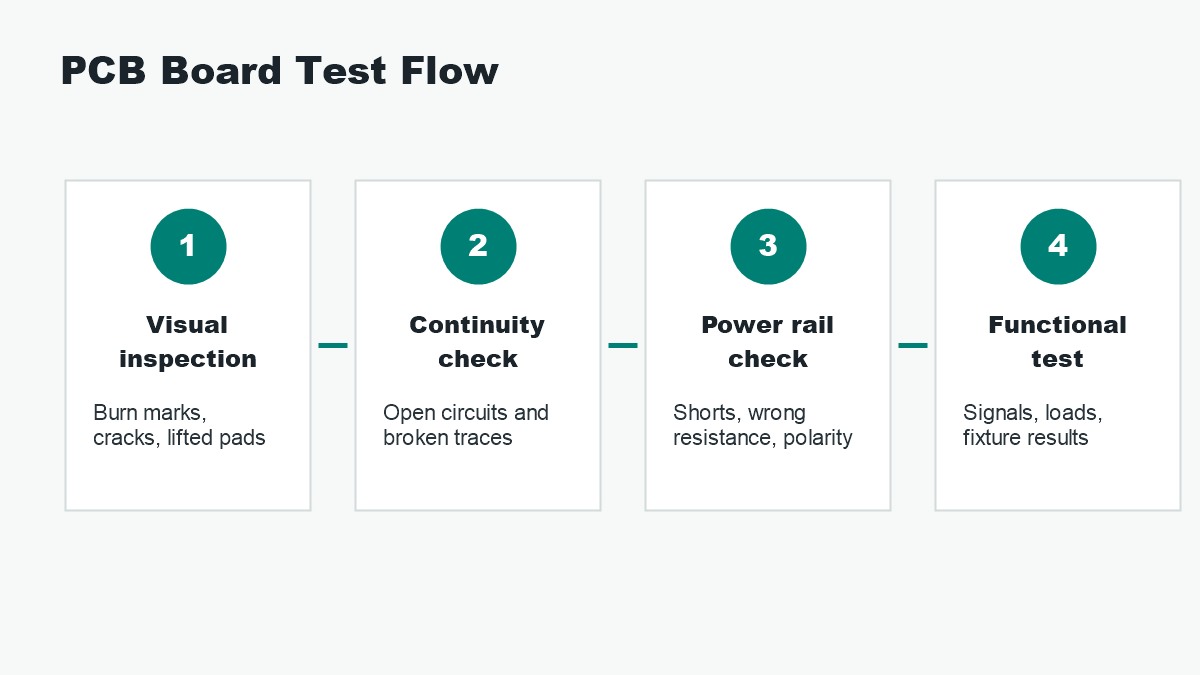
Basic PCB Board Testing Flow
A reliable test flow moves from low-risk checks to powered tests. This reduces the chance of damaging the board while still finding open circuits, shorts and functional defects.
A simple PCB board test flow starts without power and moves toward functional verification.
Test stage
Main purpose
Typical tool
Common finding
Visual inspection
Find obvious assembly and damage problems
Light, microscope, inspection camera
Solder bridge, cracked part, corrosion, lifted pad
Continuity test
Confirm a path is connected
Digital multimeter
Broken trace, open via, bad connector pin
Resistance or short check
Find abnormal low resistance before power-up
Digital multimeter
Shorted rail, wrong component, solder bridge
Power rail check
Confirm supply voltage and current behavior
Bench supply, multimeter, oscilloscope
Low rail voltage, overcurrent, unstable regulator
Functional test
Verify the board works in its intended circuit
Fixture, firmware, load, system test
Signal error, communication fault, intermittent failure
How to Test a PCB Board with a Multimeter
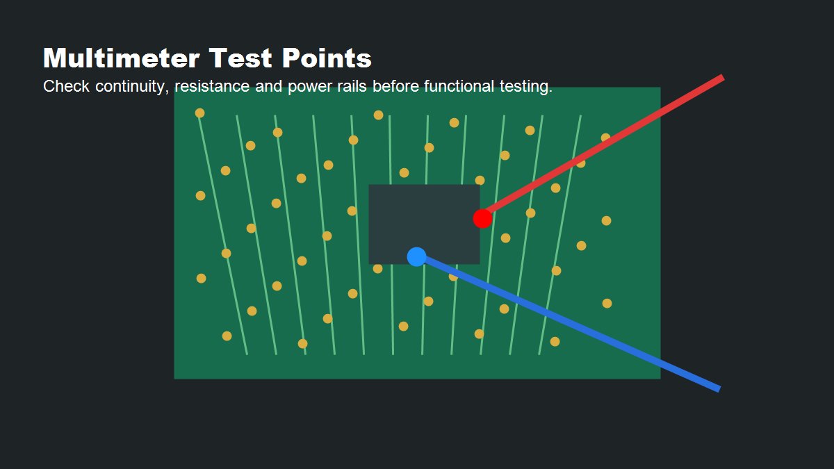
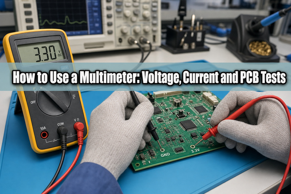
A multimeter is useful for continuity, resistance, diode checks and basic voltage checks. It is not enough for every fault, but it is usually the first practical tool for board-level troubleshooting.
With power off, use continuity mode to check suspected traces, connectors, fuses, switches and test points. Use resistance mode to compare power rails against ground. A very low resistance reading on a rail may indicate a short, but the normal value depends on the circuit, connected ICs and onboard capacitors.
With power on, use DC voltage mode to check input voltage, regulator outputs, reference rails and connector pins. Always place the black probe on a known ground point and keep the red probe steady to avoid slipping across adjacent pins.
Multimeter checks are useful for continuity, resistance, diode direction and DC rail verification.
How to Check for Shorts Before Powering the PCB
Before applying power, check the main power inputs and low-voltage rails for abnormal shorts to ground. This is one of the safest ways to prevent damage during first power-up.
Measure resistance from each rail to ground and compare it with the expected circuit behavior. A microcontroller core rail, high-current processor rail or LED driver output may naturally show low resistance, so do not assume every low value is a fault. The better method is to compare with a known-good board, schematic expectation or design engineer feedback.
If a rail reads nearly zero ohms, inspect nearby capacitors, IC pins, solder joints, vias and connectors. For repair work, current-limited power injection and thermal observation can help locate the hot component, but this should be done carefully to avoid damaging the PCB.
How to Test PCB Continuity and Broken Traces
Continuity testing confirms whether two points are electrically connected. It is useful for checking traces, vias, connectors, fuses, jumpers and repair wires.
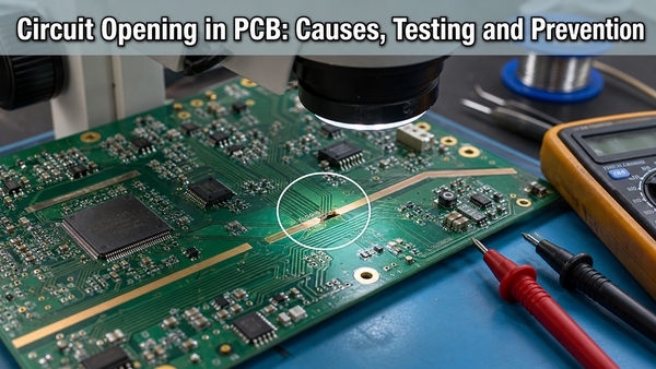
Place one probe at the starting point and the other at the expected connected point. A beep or low resistance usually means the connection exists. No beep can indicate a broken trace, damaged via, cold solder joint, cracked connector pin or wrong test point.
For dense boards, do not drag probes across fine-pitch pins. Use sharp probe tips, stable magnification and the schematic or netlist when available. On multilayer boards, a broken internal trace is harder to confirm without design files, X-ray inspection or specialist failure analysis.
How to Test Components on a PCB Board
Some components can be checked in circuit, but many readings are affected by parallel paths. Treat in-circuit component testing as a screening step, not always a final diagnosis.
Resistors can often be measured if the surrounding circuit does not create a lower parallel path. Diodes and LEDs can be checked with diode mode, but driver ICs and protection circuits may affect the reading. Capacitors may show charging behavior on a resistance range, but accurate capacitance or ESR testing usually needs a suitable meter and sometimes removal from the circuit.
ICs are harder to test directly with a multimeter. For IC-related faults, check supply pins, reset pins, clock behavior, enable pins, communication lines and output signals. An oscilloscope or logic analyzer is usually needed when the failure is dynamic.
Power-Up Testing: What to Watch
Power-up testing should use controlled voltage and current limits whenever possible. A bench power supply with current limiting can prevent a short from destroying traces, regulators or ICs.
Start with the correct input voltage and a conservative current limit. Watch current draw, smell, heat, LED behavior and voltage stability. If the current immediately hits the limit, disconnect power and return to short-circuit checks. If the current looks normal, verify each regulated rail and then check the board under its expected load.
For production boards, a test fixture is better than manual probing. A fixture can contact defined test pads, reduce operator error and record pass/fail results more consistently.
Functional Testing for PCB Boards
Functional testing checks whether the PCB performs its intended job, not only whether traces and voltages exist. This is the step that connects electrical checks with real product behavior.
Typical functional tests include firmware loading, communication checks, sensor input response, relay output, LED output, motor drive, RF response, display behavior or load testing. The correct test depends on the product. A power supply PCB needs load and ripple checks; a control board needs input-output logic checks; a communication board needs interface and signal checks.
For PCB assembly production, functional testing should be documented with fixtures, test limits, firmware version, sample records and failure codes. Without records, repeated failures become harder to trace back to design, assembly or component problems.
Common PCB Board Faults Found During Testing
PCB testing often finds a small set of recurring problems. Knowing these failure patterns helps engineers choose the right next test instead of guessing.
Orientation check, current check, schematic review
PCB Testing Checklist Before Production
For production or supplier acceptance, PCB board testing should be repeatable. A clear checklist helps avoid depending on one engineer’s memory.
Confirm PCB revision, BOM revision and assembly drawing match the order.
Inspect solder joints, polarity marks, connector orientation and visible damage.
Check main input rail resistance before power-up.
Check continuity for critical nets, connectors, fuses and test pads.
Power the board with current limiting during first validation.
Measure all required voltage rails under normal load.
Verify clocks, reset lines, enable signals and communication interfaces when relevant.
Run firmware, fixture or product-level functional tests.
Record failure symptoms, measured values and repair actions.
Feed repeated failures back into DFM, DFT, assembly and supplier review.
When Do You Need Professional PCB Testing?
Professional testing is useful when manual checks cannot explain the failure, when the board is high value, or when the issue may affect production quality.
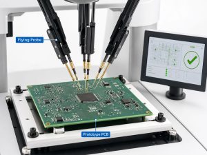
Manual multimeter checks are enough for many simple continuity and power faults. But dense multilayer PCBs, BGA assemblies, impedance-sensitive boards, high-current boards and intermittent failures often need AOI, X-ray, ICT, flying probe testing, boundary scan, functional fixtures or failure analysis support.
If the same defect appears across many boards, do not treat it as a one-off repair issue. It may come from stencil design, reflow profile, component substitution, layout weakness, fixture error, contamination or handling damage.
FAQ
How do you test a PCB board quickly?
Start with visual inspection, then use a multimeter to check shorts, continuity and main power rails. If the board passes those checks, power it with current limiting and run the intended functional test.
Can you test a PCB board with only a multimeter?
You can find many basic faults with a multimeter, including open traces, shorts, wrong resistance and missing DC voltages. Dynamic signal, firmware, timing and communication problems usually need an oscilloscope, logic analyzer or functional test fixture.
What multimeter mode is used for PCB testing?
Use continuity mode for connected paths, resistance mode for rail-to-ground checks, diode mode for diode junctions and DC voltage mode for powered rail checks. Choose the mode based on the fault you are trying to confirm.
How do you know if a PCB is bad?
A PCB may be bad if it has visible damage, abnormal rail resistance, missing voltage, excessive current draw, failed continuity, overheating parts or failed functional output. One symptom is rarely enough; confirm with a structured test sequence.
Should you power a PCB before checking for shorts?
No. Check critical power rails for shorts before applying power, especially on repaired boards, new prototypes and boards with visible solder issues. This reduces the risk of burning traces or damaging ICs.
What is the difference between PCB inspection and PCB testing?
Inspection looks for visible defects such as solder bridges, cracks and wrong orientation. Testing measures electrical behavior, continuity, voltage, current and function. A reliable quality process usually needs both.
Can a PCB pass visual inspection but still fail testing?
Yes. A board can look clean but still have hidden open vias, wrong component values, internal layer problems, firmware issues or signal faults. Visual inspection is only the first layer of quality control.
What tools are commonly used to test PCB boards?
Common tools include a microscope, digital multimeter, bench power supply, oscilloscope, logic analyzer, test fixture, AOI system, flying probe tester, ICT fixture and functional test station.
Final Thoughts
Testing a PCB board is safest when the process moves from visual checks to unpowered electrical checks, then controlled power-up and finally functional verification. This order helps catch obvious faults early while protecting the board from avoidable damage.
If you need PCB fabrication, PCB assembly, prototype validation or production support, BestPCBs can help review manufacturing requirements, testing needs and assembly risk before your board moves into mass production. Contact the engineering team at sales@bestpcbs.com for technical support and a quote.
Printed circuit board inspection is the process of checking PCB quality before, during, and after manufacturing or assembly. It helps confirm that the board matches the design files, IPC requirements, customer specifications, and the real operating needs of the final product.
At EBest Circuit (Best Technology), printed circuit board inspection is handled as part of the full manufacturing workflow. With 20 years of PCB and PCBA manufacturing experience, our team combines DFM review, fabrication control, AOI, X-ray inspection, electrical testing, and assembly quality checks to support reliable production from prototype to mass production. If you are looking for a PCB or PCBA manufacturing partner with reliable inspection and full-process quality support, please feel free to send your Gerber files, BOM, and assembly drawings to sales@bestpcbs.com. Our engineering team will be glad to review your project requirements and provide suitable manufacturing support.
What Is Printed Circuit Board Inspection?
Printed circuit board inspection is a quality control process used to examine whether a PCB or PCBA meets the required design, manufacturing, and assembly standards. It may be applied to bare PCBs, assembled circuit boards, first article samples, incoming boards, or finished electronic modules.
For bare PCBs, inspection usually focuses on the board structure and fabrication quality. This includes board dimensions, layer count, copper thickness, hole size, solder mask alignment, surface finish, silkscreen clarity, routing accuracy, impedance requirements, and electrical continuity.
For PCB assembly, inspection becomes more component-focused. The factory checks whether each component is placed correctly, soldered properly, and free from visible or hidden defects. SMT placement, polarity, BGA soldering, through-hole solder joints, connector alignment, and cleanliness are all important checkpoints.
In simple terms, PCB inspection answers four important questions:
Does the board match the Gerber files, BOM, and assembly drawings?
Are there any visible or hidden defects?
Can the board pass electrical and functional requirements?
Is the product ready for shipment or the next production stage?
A good inspection process should not rely on only one method. Visual inspection, AOI, X-ray inspection, electrical testing, and functional testing all serve different purposes. When used together, they give a more complete view of board quality.
What Should Be Included in a Printed Circuit Board Inspection Checklist?
A printed circuit board inspection checklist should cover the most important items that affect PCB reliability, assembly yield, and final product performance. The checklist can vary depending on board type, industry, material, and application, but several core items are commonly used in professional PCB and PCBA production.
For bare PCB inspection, the checklist usually includes:
Barcode, serial number, revision, traceability information
Functional result
Whether the assembled board performs as required
The checklist should be clear enough for operators, inspectors, and engineers to follow. It should also match the product’s risk level. A simple consumer control board may need standard checks, while a medical device PCBA or automotive control board may require stricter documentation, traceability, and testing control.
What Are the Key Printed Circuit Board Inspection Criteria?
Printed circuit board inspection criteria are the standards used to judge whether a PCB or PCBA is acceptable. In professional manufacturing, the inspection team should not make decisions based only on personal experience. They need defined acceptance criteria.
Common inspection criteria include IPC standards, customer drawings, Gerber files, assembly drawings, BOM, test procedures, approved samples, and internal quality documents.
For bare PCB fabrication, common criteria may include:
Correct board material and thickness
Correct copper weight
Accurate hole size and location
Proper plating thickness in through holes
Clean solder mask registration
No open circuits or shorts
Controlled impedance within tolerance when required
No delamination, blistering, serious scratches, or contamination
Board warpage within acceptable range
For PCB assembly, common criteria may include:
Correct component value and package
Correct component direction and polarity
Acceptable solder joint shape
No solder bridging between pads
No tombstoning, missing parts, or shifted components
No cracked ceramic capacitors or damaged ICs
Acceptable BGA void ratio based on product requirements
Clean board surface after soldering
Passed electrical or functional test
IPC-A-600 is often referenced for bare PCB acceptability, while IPC-A-610 is widely used for assembled board acceptability. For soldering workmanship, IPC J-STD-001 is also commonly used. In real production, these standards are often combined with customer-specific requirements.
The most important point is consistency. A good PCB manufacturer should apply the same inspection criteria across engineering review, production, quality control, and outgoing inspection. This helps avoid inconsistent judgment and reduces disputes after shipment.
How Is Incoming Inspection for Printed Circuit Boards Done?
Incoming inspection for printed circuit boards is the process of checking PCBs or components before they enter assembly or production. It is especially important when bare PCBs are produced in one facility and assembled in another, or when customers supply their own boards.
For PCB assembly projects, incoming PCB inspection helps confirm whether the bare boards are ready for SMT production. If board issues are found only after solder paste printing or reflow soldering, the cost of correction becomes higher.
A typical incoming inspection process may include:
Checking the packing condition
Confirming part number, revision, quantity, and date code
Reviewing the certificate of conformity or quality report
Checking PCB dimensions and thickness
Inspecting solder mask and surface finish
Checking warpage before SMT assembly
Confirming panel design and fiducial marks
Reviewing special requirements such as impedance, via plugging, or heavy copper
Performing sample electrical checks if needed
For components used in PCBA production, incoming inspection may include label verification, moisture sensitivity level control, package condition, quantity confirmation, and traceability record review. For high-risk or high-value components, X-ray inspection, decapsulation, or functional testing may be used when required.
At EBest Circuit (Best Technology), incoming inspection is not treated as an isolated receiving step. Because our PCB fabrication and PCBA assembly are coordinated within the same manufacturing workflow, our engineering and production teams can connect bare board quality, assembly requirements, and project documentation before SMT production begins.
Before assembly starts, our team reviews the PCB, BOM, Gerber files, pick-and-place files, and assembly drawings together. This helps us check whether the fabricated boards match the assembly requirements and identify potential mismatches early, such as pad design issues, unclear polarity marks, unsuitable footprints, panel design concerns, fiducial problems, or component availability risks.
Incoming inspection is the first quality gate before assembly. At EBest Circuit (Best Technology), it works together with DFM review, production preparation, and process control. This integrated approach helps prevent unsuitable boards or incorrect materials from entering the SMT line, improves assembly yield, and supports more stable PCB and PCBA manufacturing quality.
What Is First Article Inspection for Printed Circuit Boards?
First article inspection, often called FAI, is the detailed inspection of the first completed board or first production batch before full-scale production continues. It is an important step in PCB assembly because it confirms whether the manufacturing setup is correct.
In PCB assembly, first article inspection usually checks whether the first assembled PCBA matches the BOM, placement file, assembly drawing, polarity requirements, and customer specifications. This is especially useful for new products, engineering changes, new suppliers, or production line transfers.
A first article inspection may include:
BOM verification
Component value confirmation
Component orientation check
Reference designator check
Polarity confirmation
SMT placement accuracy
Solder joint inspection
AOI result review
X-ray inspection for BGA, QFN, LGA, or hidden solder joints
Electrical test or functional test
Label and revision confirmation
FAI is highly valuable because many assembly errors are setup-related. For example, a feeder may contain the wrong part, a component direction may be interpreted incorrectly, or a polarity mark may be unclear on the silkscreen. If this type of issue is not found during the first article stage, the same defect may repeat across the whole batch.
For high-reliability products, first article inspection also supports documentation and traceability. It provides a record that the first build was reviewed and approved before volume production moved forward.
EBest Circuit (Best Technology) uses first article inspection as part of PCBA quality control for prototype, small-batch, and production projects. For complex boards, especially those with BGA, fine-pitch ICs, mixed SMT and through-hole parts, or special materials, FAI helps engineers and customers confirm the build before scaling up.
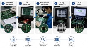
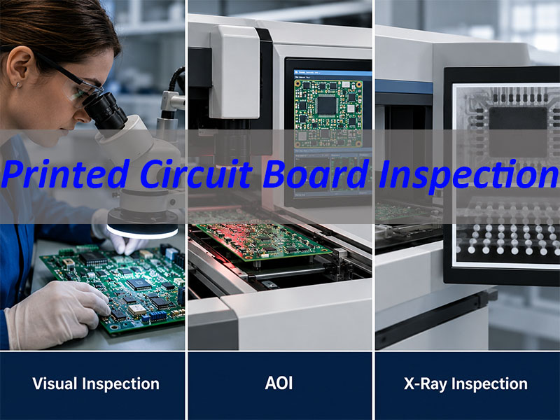
How Do Visual Inspection, AOI, and X-Ray Inspection Work in PCB Assembly?
Different inspection methods are used at different stages of PCB assembly. Each method has its own role. A strong quality control process does not depend on only one inspection tool.
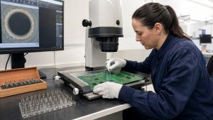
Visual inspection is usually performed by trained inspectors. It is useful for checking obvious assembly issues, solder joint appearance, component polarity, connector alignment, solder balls, contamination, broken parts, and board handling damage.
Visual inspection is flexible and practical, especially for prototypes and small-batch production. However, it depends on human judgment and cannot fully detect hidden solder defects under BGA, QFN, LGA, or bottom-terminated components.
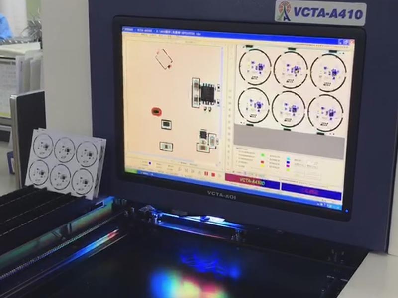
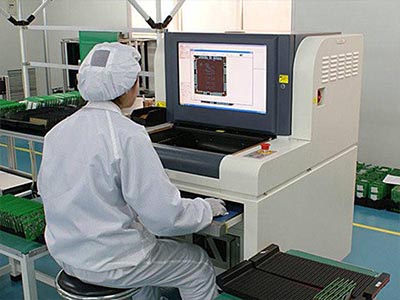
AOI, or automatic optical inspection, uses cameras and image analysis to inspect assembled boards. It is commonly used after SMT placement and reflow soldering. AOI can detect missing components, wrong polarity, component shift, tombstoning, solder bridging, insufficient solder, and some solder joint defects.
AOI is faster and more consistent than manual inspection. It is very useful for repeated production because the inspection program can compare each board against the approved standard. For boards with many small SMT parts, AOI improves inspection speed and reduces human error.
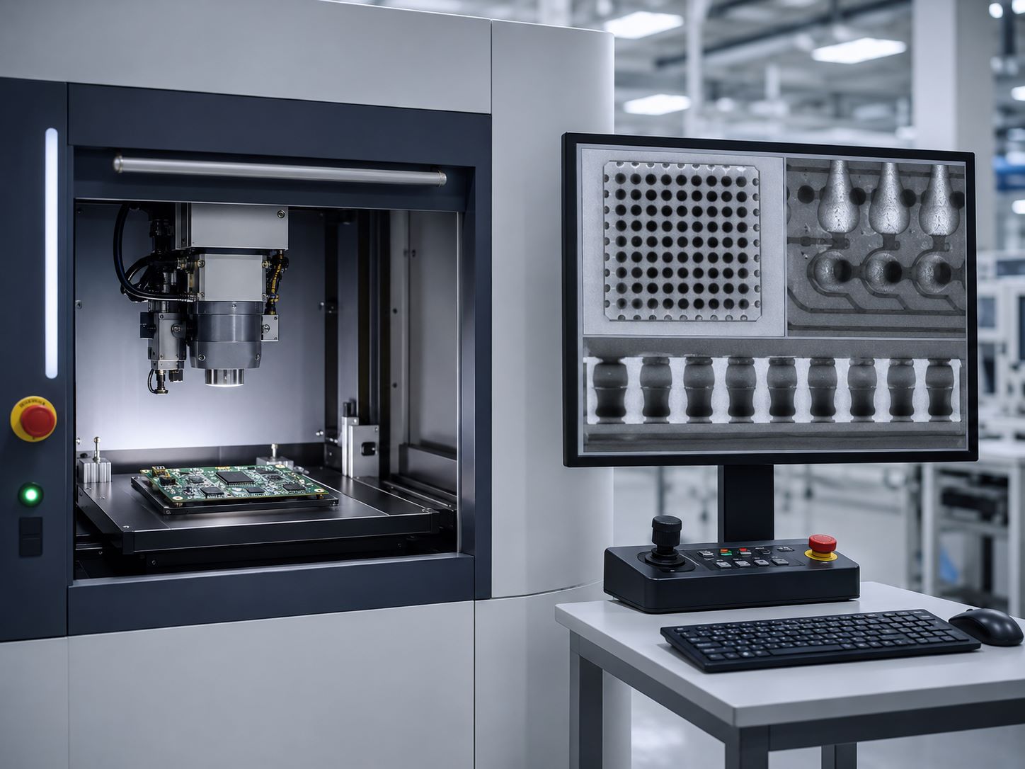
X-ray inspection is used when solder joints are hidden under the component body. It is commonly applied to BGA, QFN, LGA, bottom-terminated components, power devices, and some high-density PCB assemblies.
X-ray inspection can help detect:
BGA solder voids
Hidden solder bridges
Open solder joints
Head-in-pillow defects
Insufficient solder under hidden pads
Misalignment of hidden solder balls
Internal connection problems
For advanced PCB assembly, AOI and X-ray often work together. AOI checks visible defects quickly, while X-ray checks areas that optical inspection cannot see. Electrical testing and functional testing can then verify whether the circuit works as intended.
EBest Circuit (Best Technology) applies suitable inspection methods based on product structure, component package, and customer requirements. A simple LED PCB may not require the same inspection plan as a medical PCBA or an automotive electronic control board. The inspection method should match the risk level of the product.
What Defects Can Be Found During Printed Circuit Board Defect Inspection?
Printed circuit board defect inspection helps identify problems that may affect assembly yield, electrical performance, or long-term reliability. These defects may come from PCB fabrication, component mounting, soldering, handling, or material storage.
Cleanliness or reliability concern in sensitive products
Some defects are easy to see. Others are difficult to detect without proper equipment. For example, a solder bridge between fine-pitch IC pins may be visible under magnification, but a head-in-pillow issue under a BGA may require X-ray inspection.
Defect inspection should also connect with root cause analysis. Finding a defect is only the first step. The factory should understand why the defect happened. Was the solder paste stencil opening unsuitable? Was the reflow profile incorrect? Was the PCB surface finish oxidized? Was the component moisture-sensitive and not stored properly?
A mature PCB manufacturer uses inspection results to improve the process. This is where manufacturing experience becomes important. The real value is not only detecting problems, but also preventing the same problems from repeating in the next batch.
FAQs About Printed Circuit Board Inspection
1. Why is printed circuit board inspection important? Printed circuit board inspection helps detect fabrication and assembly defects before the product reaches the customer. It reduces rework, improves reliability, and supports stable production quality.
2. When should PCB inspection be performed? PCB inspection should be performed during incoming material control, bare board fabrication, first article inspection, PCB SMT assembly, soldering, testing, and final outgoing quality control.
3. What is the difference between PCB inspection and PCBA inspection? PCB inspection usually refers to checking the bare printed circuit board. PCBA inspection checks the assembled board after components have been mounted and soldered.
4. What is included in a PCB inspection checklist? A PCB inspection checklist may include board dimensions, copper thickness, hole quality, solder mask alignment, surface finish, electrical testing, component placement, solder joints, polarity, cleanliness, and final test results.
5. What is AOI in PCB assembly? AOI means automatic optical inspection. It uses camera-based image analysis to check component placement, polarity, solder bridges, missing parts, tombstoning, and other visible assembly defects.
6. When is X-ray inspection needed for printed circuit boards? X-ray inspection is used when solder joints are hidden under components, such as BGA, QFN, LGA, or other bottom-terminated packages. It helps detect hidden bridges, voids, opens, and alignment issues.
7. What standards are used for printed circuit board inspection? Common standards include IPC-A-600 for bare PCBs, IPC-A-610 for assembled boards, and IPC J-STD-001 for soldering workmanship. Customer specifications may also apply.
8. Can inspection find all PCB defects? No single method can find every possible defect. A reliable inspection plan often combines visual inspection, AOI, X-ray inspection, electrical testing, functional testing, and process control.
9. How does first article inspection help PCB assembly? First article inspection confirms that the first assembled board matches the BOM, drawings, placement files, and quality requirements before full production continues. It helps prevent batch-level mistakes.
10. How can I choose a reliable PCB inspection and assembly partner? Choose a manufacturer with PCB fabrication, PCBA assembly, DFM review, incoming inspection, AOI, X-ray inspection, electrical testing, functional testing, and traceability control. Experience with medical, industrial, automotive, aerospace, and communication electronics is also valuable for high-reliability projects.
Overall, printed circuit board inspection is not a single checkpoint at the end of production. It is a complete quality control system that runs through PCB fabrication, incoming material review, SMT assembly, soldering, testing, and final shipment.
For standard boards, inspection helps maintain stable production quality. For high-reliability products, it becomes even more important because small defects may affect safety, service life, and field performance.
EBest Circuit (Best Technology) supports PCB manufacturing and PCBA assembly with engineering-driven quality control. Our team provides DFM review, PCB fabrication, component sourcing, SMT assembly, AOI, X-ray inspection, electrical testing, functional testing, and final quality inspection for customers in medical electronics, industrial control, automotive electronics, communication equipment, aerospace, UAV, lighting, and other demanding industries.
If you are working on a PCB or PCBA project that requires reliable inspection, stable manufacturing, and full-process quality support, please feel free to send your Gerber files, BOM, and assembly drawings to sales@bestpcbs.com. Our engineering team will be glad to review your requirements and provide professional support for your project.
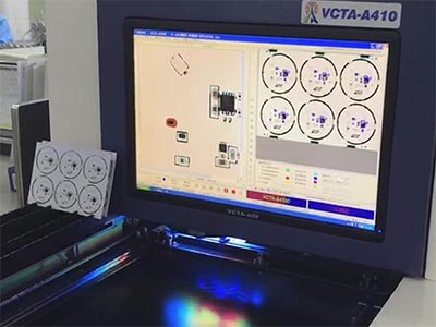
AOI technology possesses the functions of PCB inspection, solder paste printing inspection, component inspection and assembly inspection after welding. In this article, we mainly talk about PCB inspection.
PCB Inspection
PCB inspection are mainly relied on the visual inspection combined with electrical inspection during the early PCBÂ production. EBest Circuit (Best Technology), on the other hand, present many benefits of AOI testing to everyone. AOI testing is a popular choice due to the following features:
√ with the development of electronic technology, the wiring density of PCB is getting higher, which increases the difficulties in visual inspection.
√ Decrease the rate of mis-judgement.
√ Able to reduce harm to the health of inspector.
√ Save cost.
√ Avoid the electronic inspection technology can not inspect some defects.
AOI testing
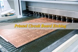
In the process of printed circuit board manufacturing, there would be some defects on the substrate fabrication and copper clad. However, these defects are mainly produced after etching. By the way, AOI testing is usually used after etching and it is utilized to find out the missing or extra part on the rigid PCB.
Most defects can be found by AOI testing (excluding the missing inspection problem), but the main problem affecting its reliability is missing inspection. The dust produced in the processing of PCB could cause false warning, so the manual inspection must be carried out after using AOI testing to detect the defects.
This website uses cookies to enhance your experience, remember your preferences, and help us understand how visitors use our site. You can accept all cookies, reject non-essential cookies, or manage your settings.
This website uses cookies to improve your experience while you navigate through the website. Out of these cookies, the cookies that are categorized as necessary are stored on your browser as they are essential for the working of basic functionalities of the website. We also use third-party cookies that help us analyze and understand how you use this website. These cookies will be stored in your browser only with your consent. You also have the option to opt-out of these cookies. But opting out of some of these cookies may have an effect on your browsing experience.
Necessary cookies are absolutely essential for the website to function properly. These cookies ensure basic functionalities and security features of the website, anonymously.
Cookie
Duration
Description
cookielawinfo-checkbox-analytics
11 months
This cookie is set by GDPR Cookie Consent plugin. The cookie is used to store the user consent for the cookies in the category "Analytics".
cookielawinfo-checkbox-functional
11 months
The cookie is set by GDPR cookie consent to record the user consent for the cookies in the category "Functional".
cookielawinfo-checkbox-necessary
11 months
This cookie is set by GDPR Cookie Consent plugin. The cookies is used to store the user consent for the cookies in the category "Necessary".
cookielawinfo-checkbox-others
11 months
This cookie is set by GDPR Cookie Consent plugin. The cookie is used to store the user consent for the cookies in the category "Other.
cookielawinfo-checkbox-performance
11 months
This cookie is set by GDPR Cookie Consent plugin. The cookie is used to store the user consent for the cookies in the category "Performance".
viewed_cookie_policy
11 months
The cookie is set by the GDPR Cookie Consent plugin and is used to store whether or not user has consented to the use of cookies. It does not store any personal data.
Functional cookies help to perform certain functionalities like sharing the content of the website on social media platforms, collect feedbacks, and other third-party features.
Performance cookies are used to understand and analyze the key performance indexes of the website which helps in delivering a better user experience for the visitors.
Analytical cookies are used to understand how visitors interact with the website. These cookies help provide information on metrics the number of visitors, bounce rate, traffic source, etc.
Advertisement cookies are used to provide visitors with relevant ads and marketing campaigns. These cookies track visitors across websites and collect information to provide customized ads.