PCB manufacturing PCB manufacturing
Home > Blog

pcb depaneling

PCB Panelization Guide: V-Score, Mouse Bites and SMT Panel Design
Friday, August 28th, 2026

PCB panelization arranges multiple circuit boards within one manufacturing panel so fabrication, solder paste printing, placement, reflow, inspection and handling can process them as a stable unit. A useful panel is not simply the layout that fits the most boards. Its outline, rails, spacing, separation method, tooling features and component clearances must match the fabricator’s CAM rules, the assembly line and the final depaneling process.
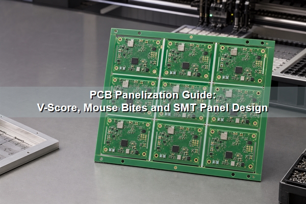
PCB panelization guide showing an SMT-ready circuit board array with rails and fiducials

What Is PCB Panelization?

PCB panelization converts one PCB design, or a controlled set of compatible designs, into a larger array that production equipment can transport and process. The finished panel normally includes the repeated board images, panel rails, separation features, global fiducials, tooling holes and identification marks. After assembly and testing, the individual boards are separated by V-scoring, routing, punching, sawing or laser cutting as appropriate.

A single PCB may be large and rigid enough to run without a delivery array, but small, narrow, irregular or thin boards often need added support. The phrase panelization construction is sometimes used for the complete arrangement of boards and temporary panel features. Practical PCB panelization guidelines must therefore define both the customer delivery panel and the fabricator-controlled production panel, which may include several delivery panels plus test coupons.

Why Is Panelizing PCB Important for Fabrication and SMT Assembly?

Panelizing PCB designs reduces repeated handling and gives conveyors, printers, placement machines and inspection systems a consistent rectangular workpiece. Several boards can pass through one stencil print, one placement program and one reflow cycle. Panel rails also protect edge components and create room for machine references that would not fit on a small finished board.

The benefit depends on the whole route. A dense array can improve laminate utilization but become too flexible under stencil pressure. A rigid array may process well yet waste material or impose excessive stress during separation. When the same supplier controls FR4 PCB fabrication and PCB assembly, CAM and SMT engineers can review the delivery panel against fabrication tolerances, stencil data, component placement and depaneling access before release.

Which PCB Panelization Methods Should You Choose?

The separation method should be chosen before the array geometry is frozen. The main PCB panelization methods have different shape, spacing, stress and edge-finish limits.

  • V-scoring: uses straight grooves from opposite sides of the panel. It is space-efficient for rectangular boards with continuous straight separation lines.
  • Tab routing: routes most of the board outline while leaving solid tabs. It supports irregular contours and allows the tabs to be cut by a router.
  • Mouse bites: add perforated holes to breakaway tabs for manual separation. A PCB panelization mouse bites pattern must match the fabricator’s drill and routing capabilities.
  • Laser depaneling: provides a narrow, non-contact cut path for suitable materials and thicknesses, but it needs specialized equipment and process review.
  • Punching or sawing: can suit stable high-volume geometries, although tooling cost or straight-line limits restrict their use.

The manufacturer should confirm channel width, residual web, tab placement and keepouts rather than relying on a universal online drawing. Material, finished thickness, copper distribution and component layout all change the result.
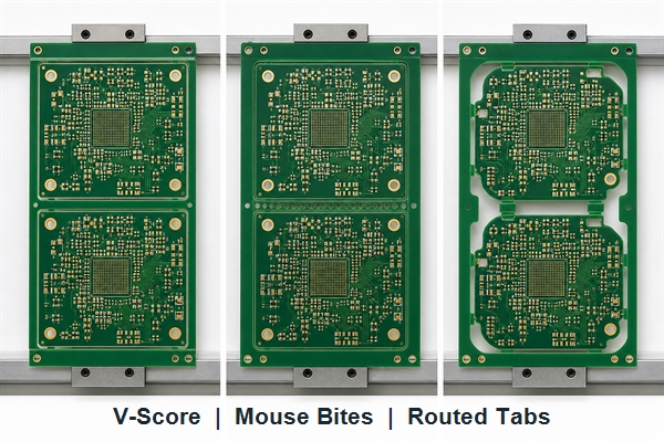
PCB panelization methods comparing V-score tab routing mouse bites and routed channels

How Do V-Score and Tab Routing Compare?

The decision starts with board geometry and permitted separation stress. V-score favors straight outlines and high panel utilization. Tab routing accepts complex shapes and controlled tab locations but consumes area for the router path.

Decision factor V-score Tab routing / mouse bites
Board outline Straight, continuous separation lines Curved or irregular outlines are possible
Board spacing Boards may share a score line Routing channel is required
Separation stress Can flex a longer board edge Localized at selected tabs
Finished edge Straight scored edge Tab witness may remain unless machine-routed flush
Component placement Needs clearance from the score and flex zone Needs clearance from tabs, router access and breakout force
Best fit Rectangular, repeatable arrays Irregular shapes and selective support points

For more detail on breakout geometry, see the related guides to mouse bites versus V-groove and V-cut PCB depaneling. The production drawing should still use the dimensions approved for the current manufacturer and equipment.

What Panel Rails, Fiducials and Tooling Holes Are Required?

Panel rails create straight conveyor edges, increase stiffness and hold temporary production features. Their width follows the printer, conveyor, fixture and depaneling setup, not a fixed internet value. Rails may also carry global fiducials, tooling holes, barcodes, coupons and orientation marks.

Global fiducials establish panel translation and rotation for vision-guided equipment. An asymmetric arrangement reduces the chance of loading the panel in the wrong orientation. Tooling holes provide mechanical registration where a fixture or process requires it. Local board fiducials may still be needed near fine-pitch BGA, QFN or other placement-critical packages.

The panel data used to manufacture an SMT stencil must use the same board step-and-repeat, origin and orientation as the placement data. A stencil generated from a single-board paste layer cannot be assumed to match a later CAM-created array unless the duplication and datum transformation are controlled.
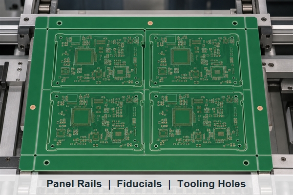
PCB panel rails with asymmetric fiducials tooling holes and SMT stencil datum features

How Should PCB Panel Size, Spacing and Component Clearance Be Set?

A reliable PCB panel design starts with the usable machine envelope, then reserves rails, separation geometry and component keepouts before calculating the array count. Filling the entire fabrication sheet first can produce a panel that cannot be printed, transported or depanelized safely.

PCB panel size is constrained by every machine that must handle the panel, including fabrication equipment, stencil printers, pick-and-place systems, reflow conveyors, AOI, test fixtures and depaneling equipment. The smallest and largest usable dimensions, conveyor direction and rail requirements should be confirmed with the actual production route.

Board-to-board spacing follows the separation tool. V-score can place straight board edges together, while routing needs a channel wide enough for the selected cutter and positional tolerance. Laser separation may use a narrower path but requires material and thermal-process review. A PCB panelization calculator can estimate how many boards fit, but it cannot see every process restriction or guarantee the lowest finished-board cost.

Component clearance must include the body, solder joints, overhang, tool envelope and expected board flex. Ceramic capacitors, BGA corners, connectors and heavy parts close to a break line deserve particular attention because depaneling strain can damage a solder joint without leaving an obvious board crack. Copper, vias and controlled-impedance structures also need clearance from score grooves, routed channels and mouse-bite holes.

When Can Different PCBs Share One Panel?

Different PCB part numbers can share a panel only when their fabrication and assembly requirements are compatible. A mixed array generally needs the same material system, layer stack, finished thickness, copper weight, surface finish, solder mask process and production quantity ratio. If one design changes, the shared panel and its assembly data may also require revision.

A homogeneous panel containing one repeated design is easier to control, inspect and replenish. A heterogeneous panel can synchronize a product set and improve material utilization, but it may create unwanted inventory if the demand ratio changes. Rotated boards can improve nesting, yet their copper distribution and component orientation should be checked for reflow, wave soldering and inspection consistency.

Rigid-flex PCB and flex PCB panelization need additional attention to stiffeners, coverlay, bend regions, tooling support and final separation. Their temporary support strategy should be reviewed as part of the material and assembly process rather than copied from a rigid FR4 grid.

What Files Define the Panelization of PCB Arrays?

The panelization of PCB arrays should be defined by one controlled data package. At minimum, identify the finished panel outline, board origins, step-and-repeat, routing or scoring paths, tabs, fiducials, tooling holes, rails and critical dimensions. The fabrication data and the drawing must agree.

  • Gerber or ODB++: copper, mask, legend, profile and panel-level production features.
  • NC drill and rout files: tooling holes, mouse bites, slots and routed channels.
  • PCB panelization drawing: overall dimensions, board arrangement, break features, datums and notes.
  • Pick-and-place data: component coordinates transformed to the panel origin and repeated orientation.
  • Paste and stencil data: the same array count and datum used by assembly.
  • Assembly drawing: panel orientation, board references, special handling and depaneling restrictions.

Do not submit a customer-created panel Gerber together with a single-board NC drill or placement file unless the relationship is explicitly controlled. Mismatched repetition counts, origins and rotations are a common source of preventable CAM and assembly questions.
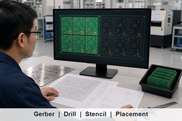
PCB panelization data review matching Gerber drill panel drawing stencil and placement origins

Which PCB Panelization Software and Tools Are Useful?

A PCB panelization tool is useful for layout exploration, but the correct choice depends on who owns the production data. PCB panelization software inside ECAD can preserve design links; CAM software can duplicate manufacturing layers, drill data and net information; a PCB panelization calculator is best treated as an early utilization estimate.

  • PCB panelization Altium workflows: Embedded Board Array and Draftsman can create repeated arrays and fabrication drawings. Searches for Altium PCB panelization and Altium Designer PCB panelization normally refer to these functions.
  • PCB panelization KiCad workflows: plugins or hierarchical layout methods can create arrays, but users should verify Gerber, drill, position and reference-designator output. The phrase KiCad PCB panelization describes the same task from the tool-first search direction.
  • Fusion 360 PCB panelization: users should confirm whether the selected Electronics/EAGLE workflow exports every required manufacturing and assembly layer for the array.
  • Free PCB panelization software: may be adequate for geometry trials, but output integrity, drill duplication, netlist consistency and revision control still require checking.
  • Manufacturer CAM: usually offers the strongest alignment with actual material utilization, routing tools, panel borders and production equipment.

Software does not know every shop-specific limit. The released files should be checked in an independent CAM viewer and approved against the manufacturer’s panel drawing.

Should You Panelize the PCB or Let the Manufacturer Do It?

Let the manufacturer create the panel when the main goal is cost-efficient fabrication and the array has no product-specific mechanical constraints. Supply clean single-board data, state whether boards must arrive as a panel or separated, identify the assembly route and approve the returned panel drawing. This lets CAM use current working-panel sizes, routing tools and process margins.

Create and control the panel yourself when the assembly fixture, test nest, barcode position, mixed-design ratio, break sequence or customer equipment requires an exact delivery format. In that case, provide both the panel data and the original single-board source, then allow a DFM review. Ownership of the layout does not remove the manufacturer’s responsibility to flag incompatible geometry.

EBest Circuit (Best Technology) lists PCB dimensions up to 610 x 610 mm, subject to stack-up, material, panel utilization and engineering review. The published PCBA process includes 3D SPI, AOI, X-ray and functional testing. Those capabilities are useful only when the approved panel, stencil, placement data and inspection program share the same revision and datum.

How Does PCB Panelization Affect Cost and Yield?

Panelization changes cost through laminate utilization, machine handling, tooling, assembly cycle time, inspection and depaneling. Increasing the number of boards per panel can reduce handling per board, but a weak or warped array can increase paste defects, placement error or breakage. The lowest material scrap is not always the lowest total cost.

Compare layouts using finished good boards per panel, expected yield and all required operations. Include routing time, score setup, tab finishing, carrier or fixture needs, stencil size, test access and the labor or machine time required to separate boards. A mixed array can reduce material waste while increasing data control and inventory risk.

What Must Be Checked Before a PCB Panel Is Approved?

Approval should freeze the panel revision that fabrication, stencil, placement, inspection and test will use. Review the panel drawing and rendered CAM output together rather than approving a dimension table in isolation.

  • Overall panel dimensions, thickness, quantity per panel and conveyor direction are stated.
  • V-score, routing channels, tabs and mouse bites match the intended depaneling process.
  • Rails, fiducials, tooling holes and orientation marks match SMT equipment and fixtures.
  • Components, copper and vias have adequate clearance from every separation feature.
  • Gerber/ODB++, NC drill, stencil, placement and assembly drawings use the same origin, rotation and revision.
  • The panel remains sufficiently rigid through printing, placement, reflow, inspection and handling.
  • Mixed designs share compatible stack-up, materials, finish and production ratio.
  • First-panel separation verifies edge quality, strain-sensitive components and fixture access before volume release.

The related PCB panelization approval guide provides a focused release-control workflow. For the present project, keep the signed panel drawing with the manufacturing package so later revisions cannot silently change the array.

PCB Panelization FAQ

What Is Meant by PCB Panelization?

What is meant by PCB panelization is the temporary grouping of multiple boards into one production unit. The boards remain connected during fabrication or assembly and are separated after the required processes are complete.

Does Every Single PCB Need a Panel?

No. A sufficiently large, rigid and machine-compatible single PCB may run without a delivery array. Small, irregular, thin or edge-sensitive boards usually benefit more from rails and repeated panel processing.

Can a PCB Panelization Calculator Produce Final Manufacturing Data?

It can estimate board count and utilization, but final data still needs routing, score, rail, tooling, fixture and equipment review. Treat the result as a layout proposal rather than automatic production approval.

Can Flex PCB Panelization Use the Same Rules as Rigid FR4?

Not automatically. Flex PCB panelization may use stiffeners, temporary carriers, tooling strips or material-specific separation methods. Bend regions, coverlay and thin-material handling require process-specific review.

Can the PCB Manufacturer Panelize Single-Board Gerbers?

Yes, and this is often the simplest route when the delivery panel has no fixed fixture constraints. State the required panel delivery, assembly process and depaneling preference, then approve the manufacturer’s drawing before production.

Conclusion

Effective PCB panelization connects board geometry with fabrication, SMT handling, separation and data control. Choose the depaneling method first, define rails and machine references, keep every production file on one datum and approve the rendered panel before release. For a DFM review of single-board or controlled panel data, contact EBest Circuit (Best Technology) at sales@bestpcbs.com.

You may also like

PCB Depaneling Guide: Methods, Process, Machines and DFM
Friday, July 17th, 2026

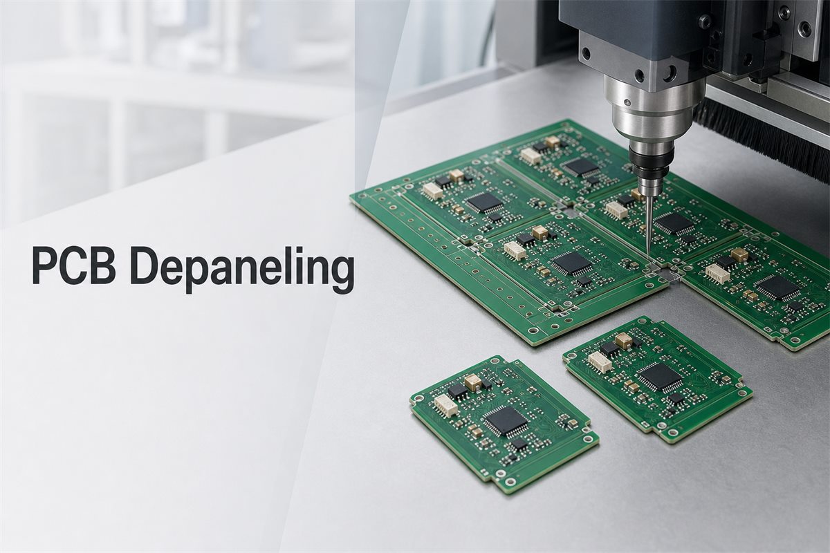
PCB depaneling is the controlled separation of individual printed circuit boards from a production panel after fabrication or assembly. The method must match the board outline, substrate, component location, production volume, edge-quality requirement, and allowable mechanical stress. A poor choice can crack components, strain solder joints, damage copper near the edge, or leave an outline that does not fit the enclosure.

The safest approach is to select the depaneling method during panel design—not after assembly is complete. V-scoring suits straight separation lines, routing supports complex outlines, laser cutting minimizes mechanical contact, and punching can be efficient for stable high-volume products. This guide explains how to choose among them and how to verify the result.

PCB Depaneling shown with a populated panel and separated circuit boards

What Is PCB Depaneling?

PCB depaneling separates finished boards from an array while protecting the assembly and maintaining the specified outline. A panel may use V-grooves, routed slots with breakaway tabs, or a fully cut path that is completed by a machine. The correct strategy depends on whether the boards are bare or populated, how close components sit to the edge, and how much bending or vibration the assembly can tolerate.

Depaneling is related to PCB profiling but is not always the same production step. Profiling creates the board outline during bare-board fabrication. Depaneling often describes final singulation of boards that remained connected for solder paste printing, component placement, reflow, testing, or handling. Once components are installed, mechanical stress becomes a more important reliability concern.

PCB Depaneling Methods Compared

The main pcb depaneling methods are V-score separation, CNC routing, laser cutting, punching, sawing, and controlled manual separation. No single method is best for every board.

Method Best Fit Main Advantage Main Risk or Limitation Key Inspection Point
V-score separation Straight board edges and regular rectangular arrays Fast separation and efficient panel use Bending stress; limited to straight score lines Score alignment, residual web, edge damage, board flex
CNC routing Complex outlines, mixed shapes, tab-routed panels Flexible path and controlled separation Dust, tool wear, vibration, cycle time Cut path, tab remnants, edge finish, fixture support
Laser cutting Thin, flexible, sensitive, or tightly constrained designs Minimal mechanical contact and precise paths Equipment cost, heat-affected material behavior, process validation Cut width, edge condition, residue, material response
Punch or die Stable, repeat high-volume geometry Short cycle once tooling is qualified Dedicated tooling and mechanical force Tool alignment, burrs, cracks, dimensional repeatability
Saw or blade Straight cuts and suitable panel access Simple linear separation Geometry limits, vibration, debris Blade condition, edge quality, contamination control
Manual breakaway Low-volume prototypes with suitable tabs or scores Little equipment investment High variation and uncontrolled bending Component damage, laminate cracks, rough tab remnants

How Does V-Score Depaneling Work?

V-score depaneling uses aligned grooves on the panel surfaces to leave a controlled web of material for later separation. It works best when every separation path is straight and can extend across the panel without running into components or irregular board geometry.

A dedicated separator supports the panel and applies a controlled shearing or rolling action along the groove. Hand snapping is possible for some prototypes, but it produces less consistent force. For detailed groove and layout considerations, see the BestPCBs guide to V-Cut in PCB and PCB depaneling.

V-scoring saves routing space because boards can share a straight boundary. The trade-off is design freedom: curves, internal corners, and non-aligned outlines need another method. Designers must also review component distance from the score and the bending direction with the manufacturer.

How Does a PCB Depaneling Router Work?

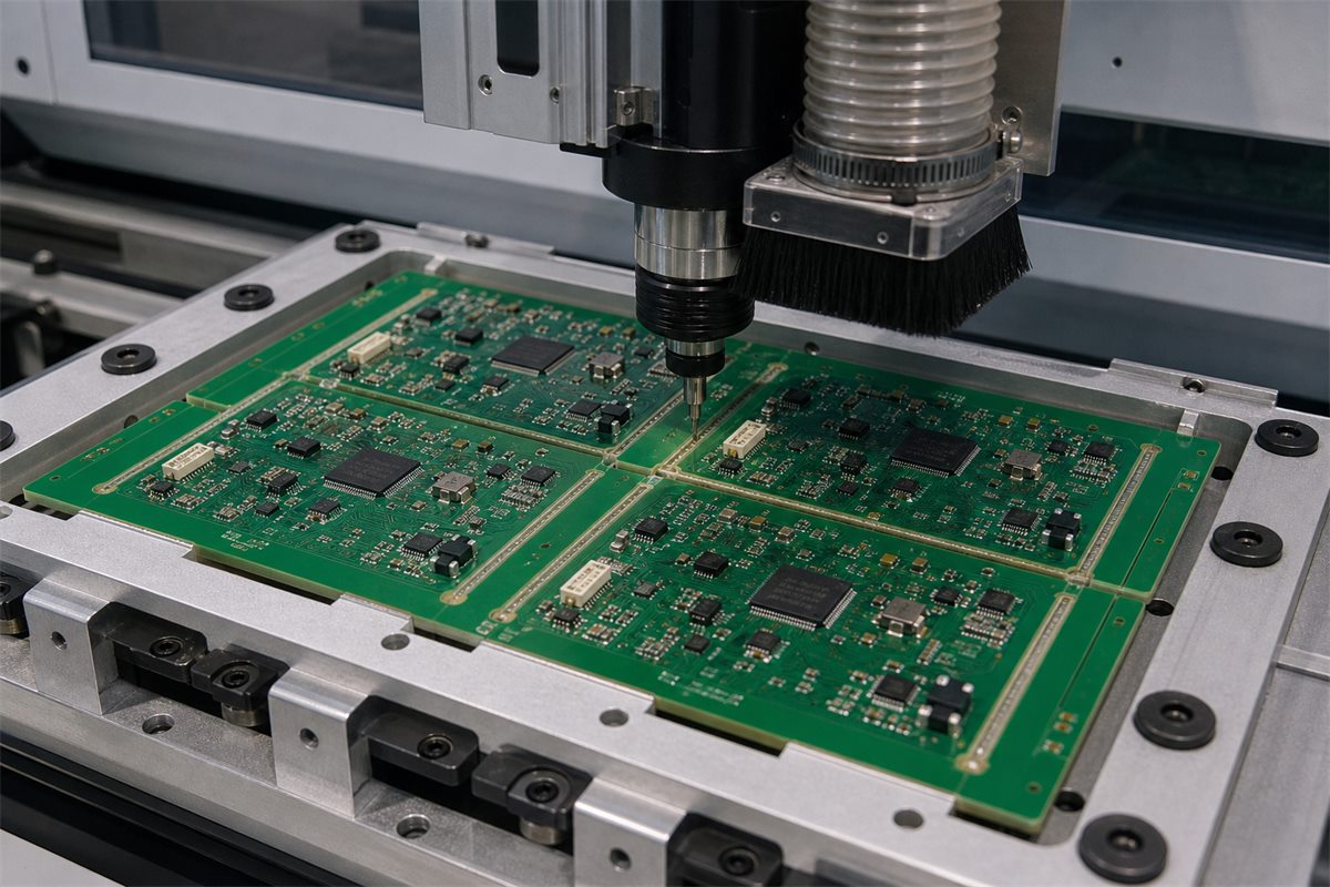
A pcb depaneling router uses a programmed spindle and cutting bit to remove tabs or follow a separation path while the panel is supported in a fixture. Routing is a strong choice for complex outlines, curved edges, cutouts, and boards that cannot use uninterrupted V-score lines.

The fixture should prevent the panel and separated boards from moving during the cut. Tool diameter, spindle condition, feed, vacuum extraction, and cut sequence affect vibration, dust, heat, and edge quality. These parameters are equipment- and material-dependent, so they should be validated with the production supplier instead of copied from a generic value.

PCB depaneling router cutting breakaway tabs from a populated panel

Router Advantages

  • Supports irregular board shapes and mixed separation paths.
  • Can cut tabs close to the final outline with controlled support.
  • Works with many rigid panel constructions when the process is qualified.
  • Allows automated programs and fixtures for repeat production.

Router Risks

  • Worn tools can create rough edges, heat, or higher cutting force.
  • Insufficient fixturing can let the board vibrate or shift.
  • Dust extraction must protect assemblies and equipment.
  • Cut sequence can release support too early and overload the remaining tabs.

When Does Laser Depaneling Make Sense?

Laser depaneling is useful when mechanical contact must be minimized or when the cut path is too fine or complex for a conventional tool. It is often considered for flex circuits, thin substrates, compact assemblies, and designs with sensitive parts near the board edge.

A laser process still requires material qualification. Wavelength, energy delivery, cut speed, number of passes, extraction, and material composition influence the result. The edge should be examined for discoloration, residue, delamination, dimensional variation, or changes that could affect cleanliness and reliability. “Contactless” does not mean “validation-free.”

Mouse Bites, Breakaway Tabs, and Panel Support

Mouse bites are rows of small holes that create a controlled weak section in a breakaway tab. They allow irregular boards to remain attached to a routed panel during assembly and handling, then separate manually or by machine. The remaining tab may need trimming when the finished edge must be flush.

Tab location matters as much as tab geometry. A tab placed beside a fragile component, connector, thin neck, antenna area, or edge copper can concentrate stress where the product is most vulnerable. The BestPCBs mouse bites PCB guide explains this panel connection method in more detail.

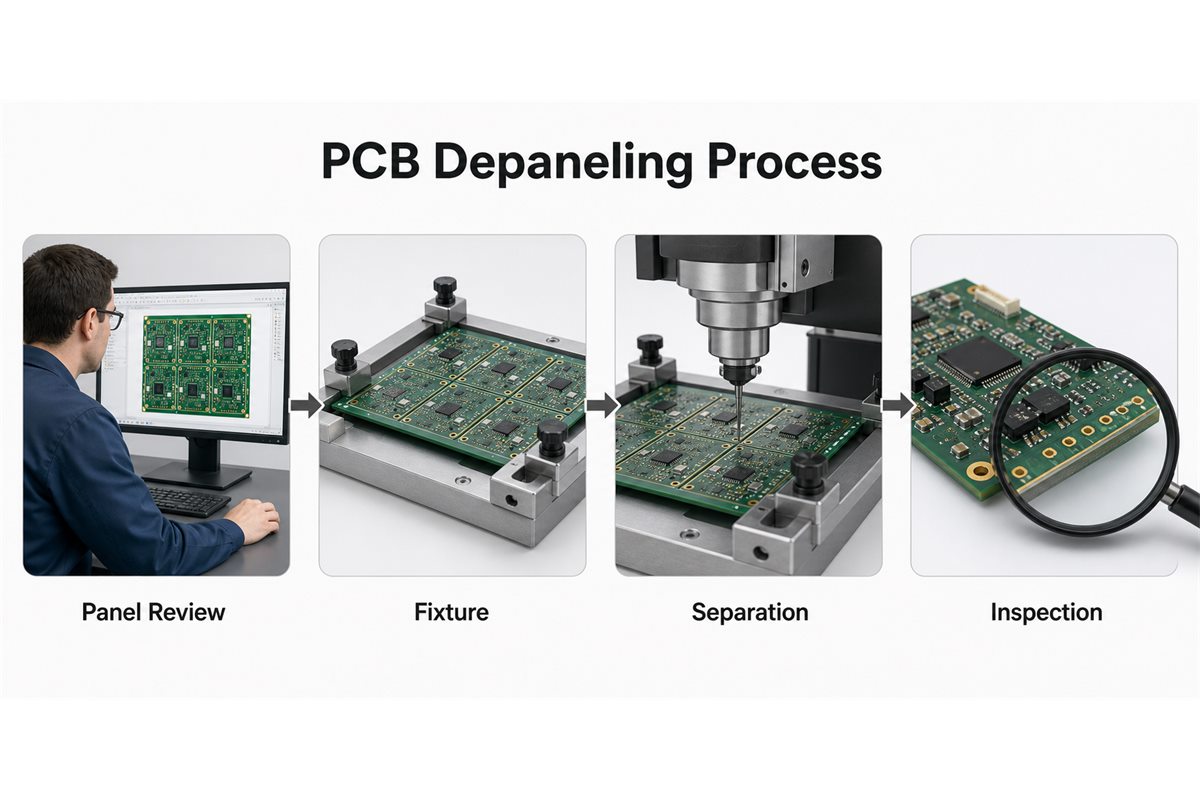
PCB Depaneling Process From Panel Review to Inspection

A controlled pcb depaneling process starts with design review and ends with documented inspection. Treating the cut itself as the entire process misses the risks created by panel support, component placement, tool condition, and post-cut handling.

  1. Review the panel drawing: Confirm board outlines, rails, fiducials, tooling holes, tabs, score lines, and keep-out areas.
  2. Identify sensitive locations: Mark ceramic capacitors, BGAs, connectors, thin sections, heavy components, edge copper, and finished surfaces.
  3. Select the separation method: Match geometry, substrate, assembly state, volume, edge quality, and stress limits.
  4. Qualify the fixture and program: Support the panel, control the cutting sequence, and keep boards stable after release.
  5. Run a controlled first article: Inspect the first separated boards before processing the full lot.
  6. Monitor the process: Check tool wear, alignment, dust extraction, cut consistency, and operator handling.
  7. Inspect finished boards: Verify outline, edge quality, tab remnants, damage, cleanliness, and electrical or functional results where required.
PCB depaneling process showing panel review routing separation and edge inspection

How Do You Choose a PCB Depaneling Machine?

A pcb depaneling machine should be selected around the real product mix and risk profile, not only advertised cutting speed. The machine must accommodate panel size, board thickness, outline complexity, substrate, component height, required support, dust control, traceability, and maintenance needs.

  • Product geometry: Straight V-score arrays need different equipment from routed complex outlines.
  • Assembly sensitivity: Review permissible bending, vibration, heat, and contamination.
  • Production mix: High-mix work values rapid program and fixture changeover; stable high-volume work may justify dedicated tooling.
  • Edge requirement: Enclosure fit, exposed customer surfaces, connectors, coating, and sealing may require tighter edge control.
  • Process control: Consider tool-life monitoring, program control, vision alignment, extraction, error handling, and production records.
  • Serviceability: Review consumables, preventive maintenance, local technical support, training, and spare-part availability.

Machine price alone is not the total cost. Fixtures, tools, extraction, programming, maintenance, floor space, cycle time, inspection, scrap risk, and changeover labor all belong in the comparison.

DFM Rules That Make Depaneling Safer

Depaneling DFM aligns the board outline, panel connection, component placement, and selected machine before production. The detailed limits should come from the PCB/PCBA supplier because material, thickness, equipment, and component sensitivity differ.

  • Define V-score lines, routed slots, and tabs clearly in fabrication and panel drawings.
  • Keep components, copper, vias, and fragile features away from separation zones according to supplier rules.
  • Use breakaway rails and tooling features that support printing, placement, reflow, testing, and separation.
  • Avoid tab placement that twists a thin board section or loads a nearby component.
  • Plan how the final released board will be supported, collected, and transferred.
  • Specify critical outline dimensions and surfaces that require flush tab removal or controlled edge finish.
  • Review mixed-material panels, metal-core boards, flex, rigid-flex, and thick copper constructions separately.

Panelization decisions have downstream effects on yield and handling. Use the BestPCBs PCB panel design guidelines and PCBA panel strategies when preparing the array.

Common PCB Depaneling Defects

Most depaneling defects come from excessive force, poor support, worn tools, incorrect geometry, or missing process control. Inspection should look beyond cosmetic edge quality.

Defect Likely Cause Why It Matters Prevention or Check
Rough edge or large tab remnant Tool wear, poor path, unsuitable tab design, uncontrolled break Enclosure interference, handling risk, exposed fibers Check tool condition, tab location, trim requirement, and outline
Laminate crack or delamination High bending force, impact, heat, or unsuitable process Mechanical weakness and possible conductor damage Improve support, reduce force, change method, inspect edges
Cracked MLCC or solder joint Board flex near the separation line Immediate or latent electrical failure Move sensitive parts, control strain, review fixture and method
Copper or via damage Features too close to the outline or cut path error Open circuits, reduced insulation, reliability loss Apply edge keep-outs and verify the programmed path
Dust or residue Routing debris, poor extraction, laser byproducts Contamination and inspection difficulty Validate extraction, cleaning, and post-process inspection

Pad cratering and component cracking can be latent. A board may pass a quick visual check but fail later after thermal or mechanical loading. Sensitive products may require strain assessment, cross-section review, electrical testing, or other validation defined by the product’s reliability plan.

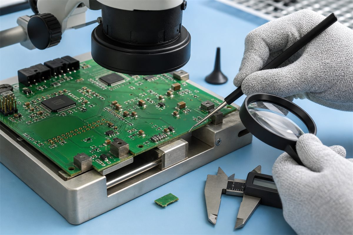
How Do You Inspect Depaneled PCBs?

Inspection should verify the board outline and detect damage caused by separation. The exact sampling plan and acceptance criteria depend on product risk and customer requirements.

  • Visual or magnified edge inspection for cracks, fibers, burrs, discoloration, and tab remnants.
  • Dimensional inspection of critical outline features, slots, notches, and connector edges.
  • Inspection of nearby components, solder joints, vias, traces, and conformal coating.
  • Cleanliness check after routing or laser processing.
  • Electrical, functional, or mechanical verification when the depaneling risk justifies it.
  • First-article approval and periodic checks for tool wear or process drift.
Magnified inspection of a depaneled PCB edge and nearby components

Special Cases: Aluminum, Flex, and Sensitive Assemblies

Special substrates and assemblies need separate process review because their cutting behavior differs from ordinary rigid FR-4. Aluminum boards combine metal and dielectric layers, flex circuits can deform during mechanical separation, and rigid-flex transitions can be vulnerable to poor support.

Metal-core products may require a saw, router, punch, or other qualified process depending on outline and thickness. Refer to the BestPCBs explanation of aluminum PCB depaneling for that specific material family. Flex and rigid-flex products often favor processes that minimize bending and control heat, but the final choice must be validated with the actual stackup and design.

What Files Should You Provide for Depaneling Review?

A useful RFQ package gives the manufacturer enough information to review both the panel and the separated board. Include:

  • Gerber X2 or ODB++ data with a clear board outline.
  • Panel drawing showing rails, tabs, V-scores, routed slots, tooling holes, and fiducials.
  • Assembly drawings and component-height information.
  • Critical edge dimensions, connector locations, and cosmetic requirements.
  • Material, finished thickness, copper construction, surface finish, and quantity.
  • Preferred depaneling method, if already qualified.
  • Known sensitive components or maximum handling/strain requirements.
  • Inspection, cleanliness, traceability, and packaging expectations.

For a new PCB depaneling process, ask the supplier to review panel connection and component placement before the assembly layout is frozen.

PCB Depaneling FAQ

What is the purpose of PCB depaneling?

It separates individual boards from a production panel while preserving board dimensions, edge quality, components, solder joints, and electrical reliability.

Which PCB depaneling method is best?

The best method depends on board shape, substrate, component proximity, production volume, edge requirement, and allowable stress. V-score is efficient for straight lines, routing supports complex outlines, and laser cutting is useful when mechanical contact must be minimized.

Can PCBs be depaneled by hand?

Some prototypes with suitable V-scores or breakaway tabs can be separated manually. However, hand breaking applies variable bending force and may damage nearby components or laminate, so controlled equipment is safer for sensitive or repeat production.

What is the difference between V-score and mouse bites?

V-score uses continuous grooves along straight separation lines. Mouse bites use perforated breakaway tabs between routed slots, allowing more flexible board shapes but leaving tab remnants after separation.

Does router depaneling damage components?

A qualified router process can limit assembly stress, but poor fixturing, worn tools, vibration, dust, or an incorrect cut sequence can still cause damage. Sensitive components and edge clearances must be reviewed during DFM.

Is laser depaneling suitable for every PCB?

No. Laser cutting offers precise, low-contact processing, but the wavelength, energy, material response, residue, heat effects, and cycle economics must be qualified for the actual substrate and product.

Why do ceramic capacitors crack during depaneling?

Multilayer ceramic capacitors can crack when board bending transfers tensile strain into the component body or solder joints. Placement, orientation, distance from the edge, fixture support, and separation method all influence the risk.

When should a punch tool be used?

Punching can suit stable high-volume designs with repeat geometry when dedicated tooling cost is justified. The tool and support must be qualified for alignment, burrs, dimensional control, and mechanical stress.

How do I reduce routing dust?

Use effective local extraction, suitable tooling, controlled process parameters, fixture design, and cleaning or inspection steps matched to the product. Dust control should be validated on populated assemblies.

Should depaneling happen before or after assembly?

It can happen at different stages. Many boards stay panelized through SMT assembly and testing for efficient handling, then are separated afterward. The later the separation, the more carefully the process must protect installed components and solder joints.

What determines PCB depaneling machine price?

Machine type, automation, panel capacity, vision, fixtures, extraction, tooling, software, traceability, service, and throughput all influence price. Compare total process cost and scrap risk, not purchase price alone.

What should be checked after depaneling?

Inspect the outline, edges, tab remnants, nearby copper, vias, components, solder joints, cleanliness, and critical dimensions. Add electrical or functional verification when product risk requires it.

Choose Depaneling Before the Panel Is Final

Reliable depaneling begins with the panel drawing, not the cutting machine. Select the connection method, component keep-outs, fixture strategy, separation sequence, and inspection plan together. A fast method that introduces board strain or edge damage is not a low-cost process once rework, scrap, and field risk are included.

If you are preparing PCB depaneling requirements for a new PCB or PCBA project, send the panel drawing, board files, assembly data, material, thickness, quantity, critical edge requirements, and sensitive-component information for DFM review. If you’re sourcing reliable PCB/PCBA manufacturing, including OEM, ODM, prototyping, mass production, or custom engineering solutions, reach out to our engineering team for technical support and a quote at sales@bestpcbs.com.

You may also like