PCB manufacturing PCB manufacturing
Home > Blog

Ceramic Core PCB | Alumina & Aluminum Nitride Ceramic PCB

May 11th, 2026

What is a ceramic core PCB?

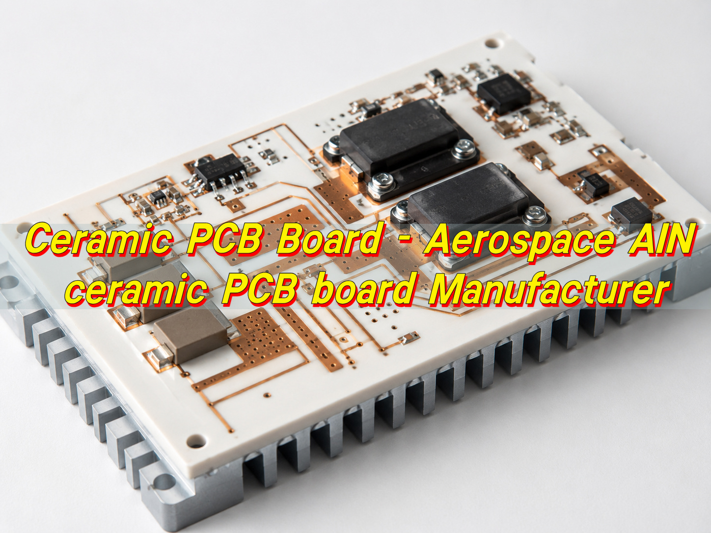
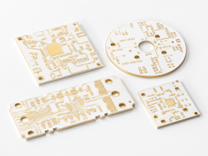
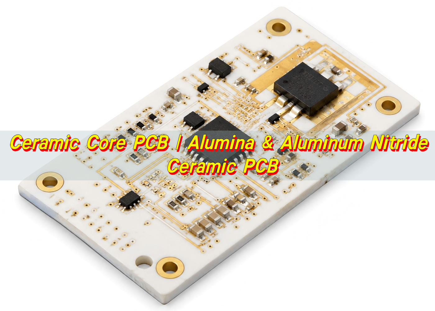
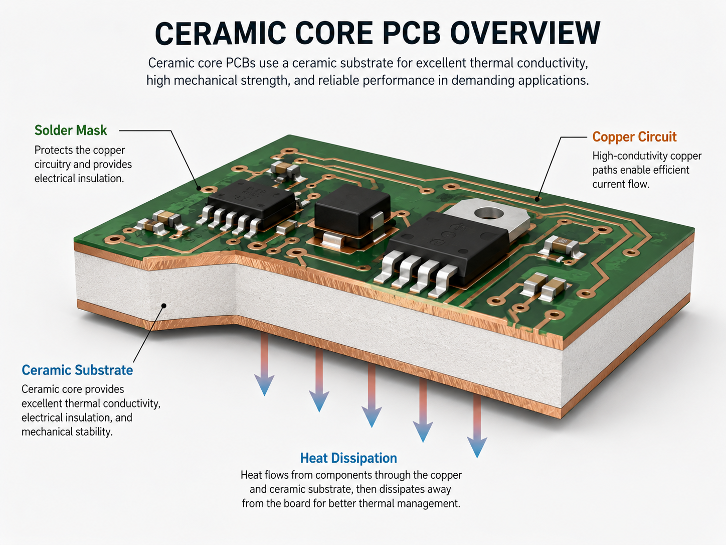
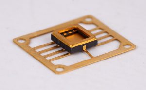
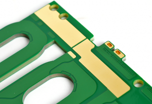
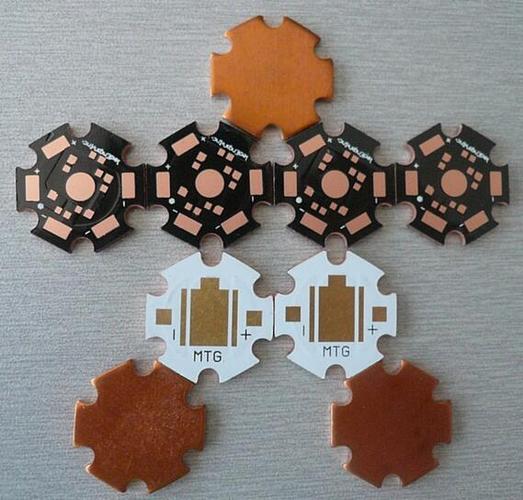
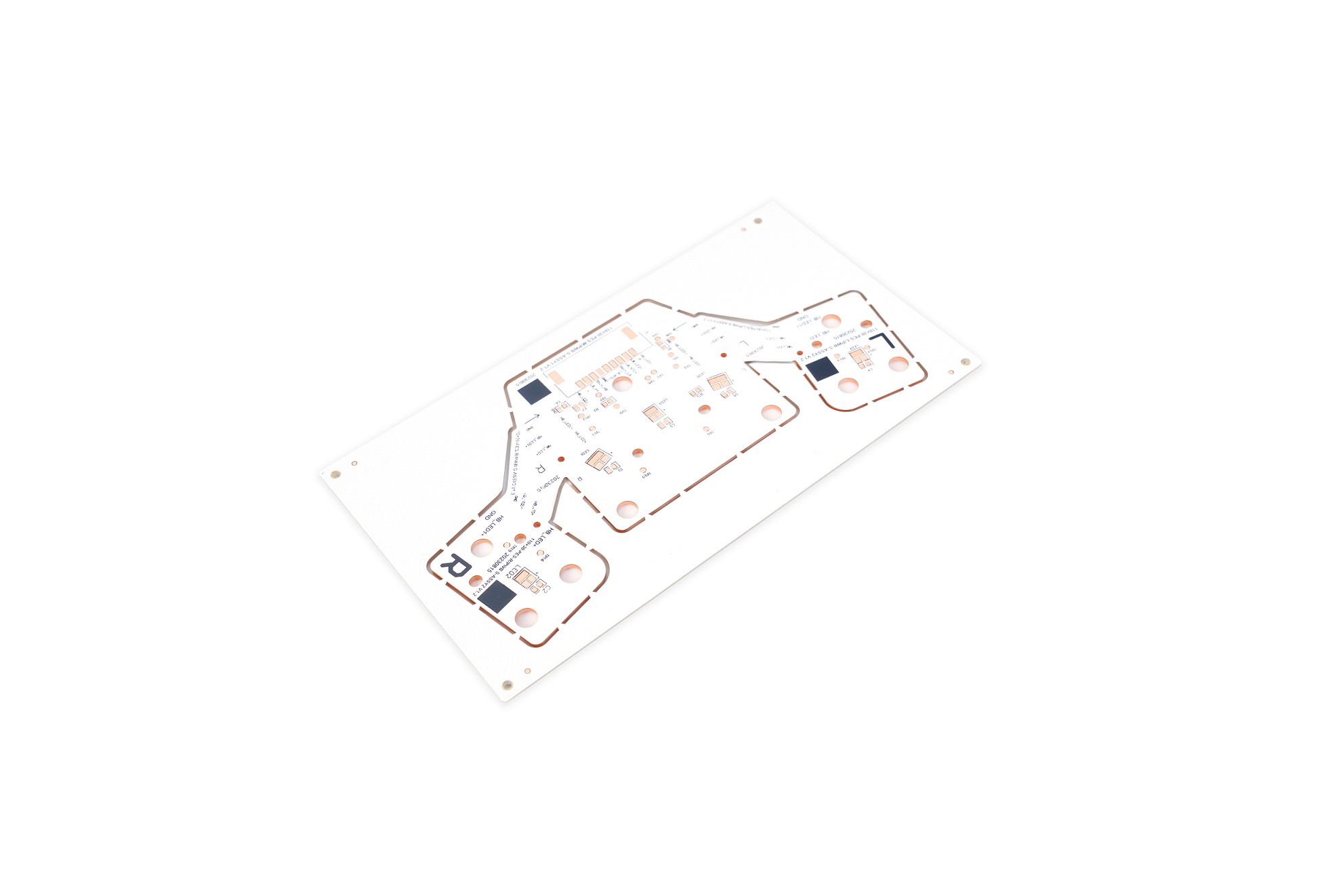
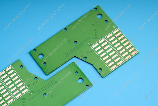
Ceramic core PCB is a printed circuit board built on a ceramic substrate instead of a conventional organic laminate such as FR4. In this type of board, the ceramic layer works as the main supporting base and thermal pathway. It gives the circuit strong heat transfer, stable electrical insulation, and excellent dimensional consistency under demanding operating conditions.

Unlike standard PCB materials that rely on glass fiber and resin, ceramic PCB boards use inorganic ceramic materials such as alumina, aluminum nitride, or silicon nitride. These materials are valued in high-power, high-frequency, high-temperature, and high-reliability electronics.

In the PCB industry, ceramic core PCB is often used for applications where ordinary laminates cannot provide enough thermal conductivity or long-term stability. The board may support thick copper, thin-film circuits, DPC copper plating, DBC bonding, or AMB structures, depending on the electrical and mechanical requirements of the project.

EBest Circuit (Best Technology) supports ceramic PCB manufacturing for engineers who need more than a basic circuit board. With experience in alumina PCB, aluminum nitride PCB, DPC ceramic PCB, DBC ceramic substrate, AMB ceramic substrate, and customized ceramic PCB boards, EBest Circuit helps customers move from early design review to production with practical engineering support.

What is the difference between ceramic and FR4?

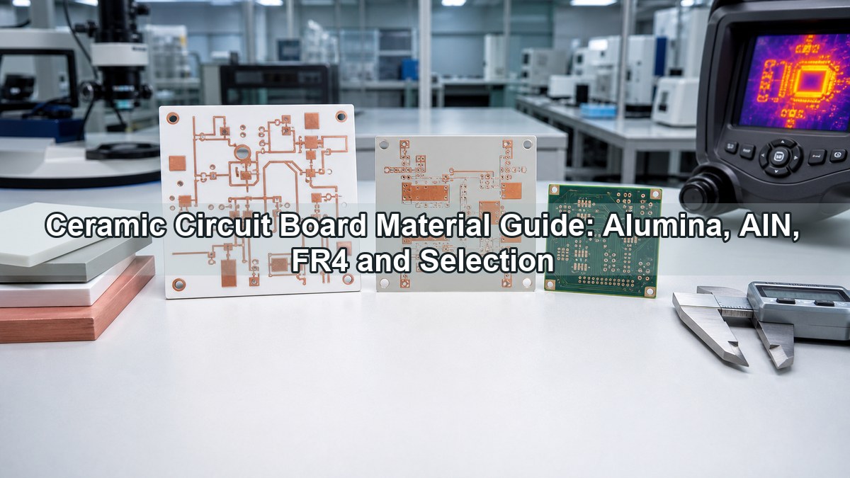
Ceramic PCB and FR4 PCB are both widely used in electronics, but they are designed for different performance levels. FR4 is the most common PCB substrate because it is cost-effective, easy to process, and suitable for many consumer, industrial, and general electronic products. Ceramic PCB is selected when the circuit needs higher thermal conductivity, better temperature resistance, and stronger dimensional stability.

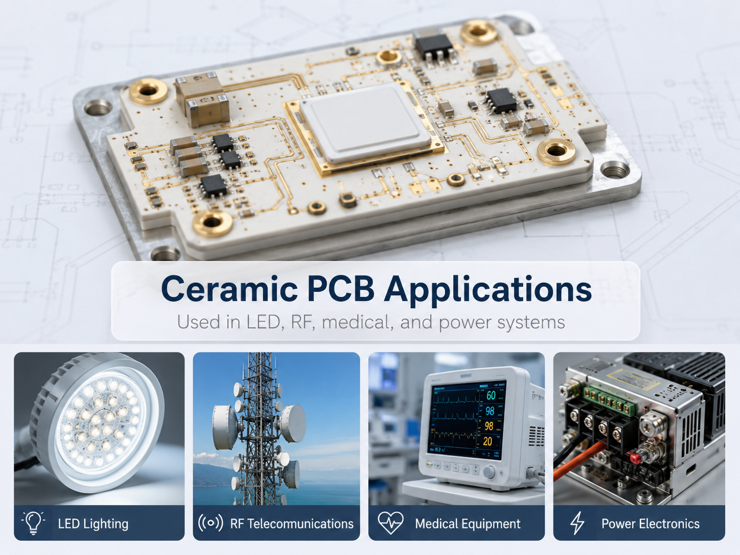
FR4 is made from woven fiberglass cloth and epoxy resin. It performs well in standard electronic assemblies, but its thermal conductivity is limited. Ceramic boards, by contrast, use inorganic ceramic substrates that conduct heat much more efficiently while keeping excellent insulation. This is why ceramic core PCB is commonly found in LED modules, laser equipment, power electronics, sensors, medical devices, automotive electronics, and aerospace-related systems.

ItemCeramic Core PCBFR4 PCB
Main materialAlumina, aluminum nitride, silicon nitride, or other ceramic materialsGlass fiber reinforced epoxy laminate
Thermal conductivityHigh, suitable for heat-sensitive and power applicationsLow to moderate, suitable for general electronics
Temperature resistanceExcellent stability at elevated temperaturesGood for standard operating environments
Mechanical behaviorHard, stable, and rigid, but requires careful handlingTougher and more flexible during standard assembly
Electrical insulationVery strong insulation performanceReliable insulation for common circuit designs
Typical applicationsHigh-power LEDs, RF modules, power devices, sensors, automotive electronicsConsumer electronics, control boards, communication devices, general PCBA
Cost levelHigher due to material and process complexityLower and highly scalable

The choice should not be based only on price. If the circuit generates a high amount of heat or must keep stable performance in a harsh environment, ceramic PCB can provide a stronger technical foundation.

What’s the difference between alumina PCB and aluminum nitride PCB?

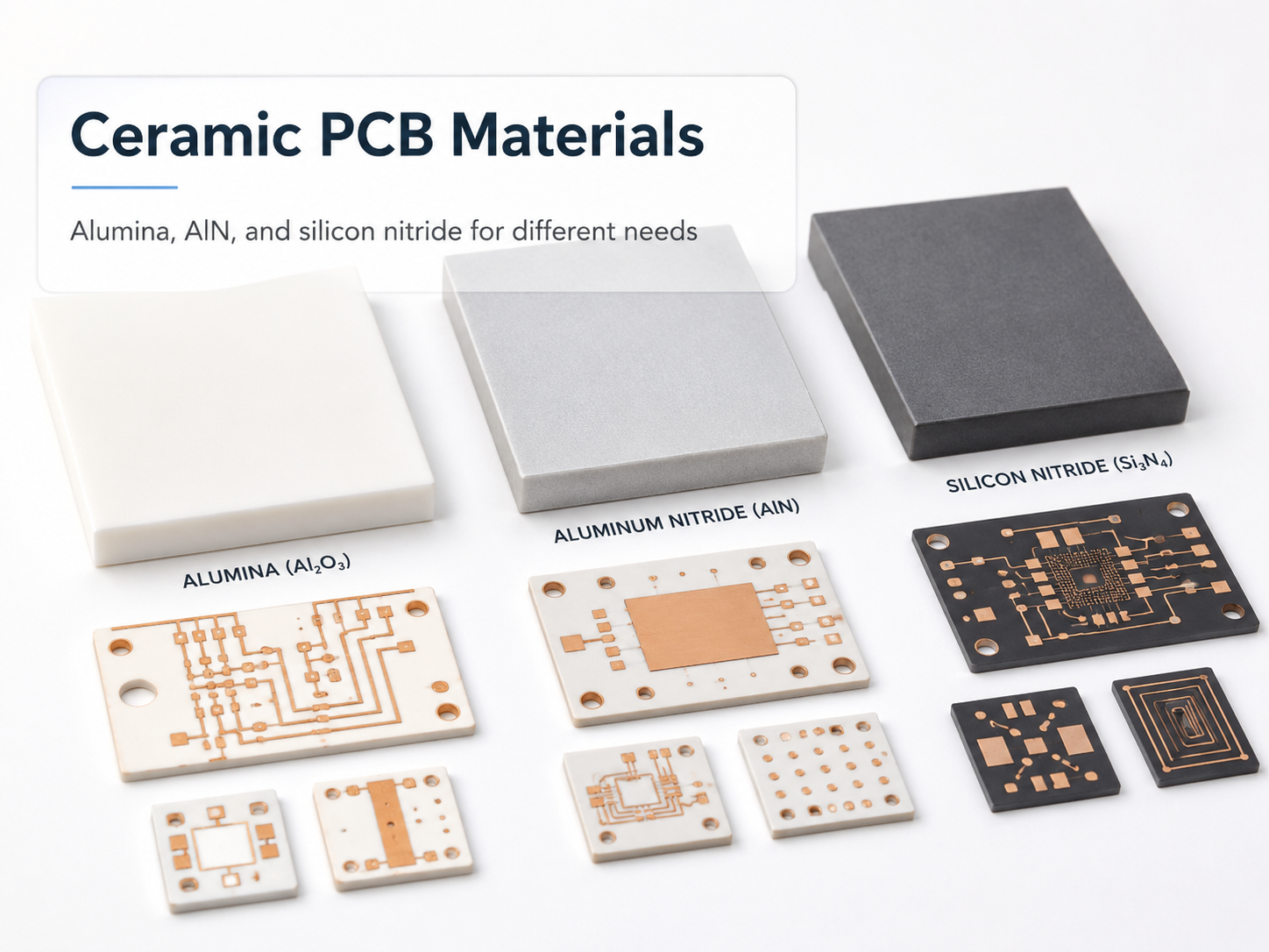
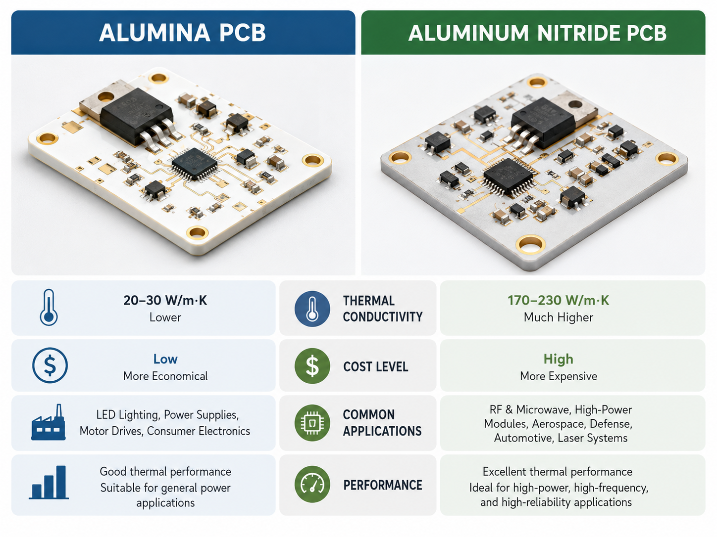
Alumina PCB and aluminum nitride PCB are two of the most common ceramic PCB materials. Both provide good insulation, stable structure, and better thermal performance than FR4. The key difference is thermal conductivity. Alumina is widely used because it offers a balanced combination of price, process maturity, and electrical performance. Aluminum nitride is chosen when the design needs much higher heat dissipation.

Alumina PCB usually refers to ceramic boards made from aluminum oxide. Common grades include 96% alumina and 99.6% alumina. It is a practical choice for many LED, sensor, power module, and industrial electronic applications. It has good mechanical strength, stable electrical insulation, and a more accessible ceramic board price compared with aluminum nitride.

Aluminum nitride PCB is often used in more demanding thermal designs. Its thermal conductivity can be several times higher than alumina, making it highly suitable for power semiconductors, high-brightness LEDs, laser diodes, automotive power modules, and compact high-power assemblies. It is usually more expensive than alumina because the raw material, sintering process, and manufacturing control are more demanding.

ItemAlumina PCBAluminum Nitride PCB
MaterialAluminum oxide ceramicAluminum nitride ceramic
Thermal conductivityGood, commonly used for medium to high thermal needsExcellent, suitable for high-power heat dissipation
CostMore economical among ceramic PCB optionsHigher due to material and process requirements
Mechanical strengthStrong and mature in productionStrong, with careful process control needed
Electrical insulationExcellentExcellent
Typical useLED modules, sensors, heaters, industrial controls, power circuitsPower modules, laser devices, high-power LEDs, RF and automotive electronics

EBest Circuit can help customers compare ceramic PCB materials during DFM review, so the final design matches both technical needs and production cost targets.

Why use ceramic PCB?

Ceramic PCB is used because it solves several practical engineering problems at the same time. It helps remove heat, keeps circuits electrically insulated, supports high-density layouts, and performs well in high-temperature environments.

One of the strongest reasons to use ceramic PCB is thermal management. As electronic products become smaller and more powerful, heat has less room to escape. If heat remains around chips, LEDs, or power components, performance can drop over time. A ceramic board gives heat a faster path away from the source, helping the assembly work in a more stable condition.

Ceramic PCB also supports excellent electrical properties. It can provide low dielectric loss, high insulation resistance, and stable performance across demanding operating conditions. This is important for RF circuits, sensor modules, high-voltage electronics, and power devices.

  • High thermal conductivity for better heat spreading
  • Strong electrical insulation for compact circuit layouts
  • Excellent temperature resistance for harsh environments
  • Stable dimensions during thermal cycling
  • Good compatibility with power devices, LEDs, sensors, and RF modules
  • Long service life in high-reliability electronic products

For manufacturers, ceramic PCB also brings value in quality consistency. The substrate has stable physical properties, which helps reduce performance drift in precision electronics. For engineers, it allows a cleaner thermal design and can reduce the need for bulky heat sinks in some compact products.

How much does a ceramic PCB cost?

Ceramic PCB cost is usually higher than standard FR4 PCB cost because the material, processing method, copper bonding, laser drilling, metallization, and quality control are more specialized. In high-power or high-reliability products, better heat transfer and longer operating stability can reduce the risk of field problems and improve product performance.

The ceramic board price depends on several technical factors. Material selection is one of the biggest cost drivers. Alumina PCB is generally more economical, while aluminum nitride PCB costs more because it provides much higher thermal conductivity. Board size, thickness, copper thickness, circuit precision, via structure, surface finish, tolerance control, and production quantity also affect the final quotation.

Cost FactorHow It Affects Ceramic PCB Cost
Ceramic materialAlumina is usually more economical; aluminum nitride is higher in cost but stronger in thermal performance.
Board sizeLarger ceramic boards use more raw material and may require tighter handling control.
Substrate thicknessSpecial thickness requirements may increase material preparation and processing cost.
Copper thicknessThicker copper improves current capacity but increases plating or bonding complexity.
Line width and spacingFine circuits require more precise manufacturing control.
Via structureFilled vias, laser vias, and conductive vias can raise process complexity.
Surface finishENIG, immersion silver, nickel gold, or other finishes may affect pricing.
Order quantityPrototype cost per piece is higher; batch production usually improves unit cost.

For a reliable ceramic PCB quotation, engineers should provide Gerber files, drawings, material requirements, board thickness, copper thickness, surface finish, tolerance needs, and expected quantity. If the design is still being evaluated, EBest Circuit can review the technical requirements and suggest a practical manufacturing route before final pricing.

Can ceramic core PCB be customized in size and layout?

Yes, ceramic core PCB can be customized in size, layout, thickness, copper pattern, surface finish, and structure. Customization is one of the main reasons ceramic PCB is used in advanced electronic products.

Custom ceramic PCB does require careful design planning. Ceramic materials are hard and stable, but they are processed differently from FR4. Features such as hole size, edge shape, slot position, via design, copper thickness, and board outline should be reviewed before production. A strong DFM check helps improve manufacturability and keeps the finished board aligned with the original electrical and thermal goals.

Common customization options include:

  • Alumina PCB or aluminum nitride PCB substrate selection
  • Custom board outline, size, and ceramic thickness
  • Single-sided, double-sided, or multilayer ceramic PCB structure
  • Thin-film or thick-film circuit design
  • DPC, DBC, or AMB ceramic core manufacturing process
  • ENIG, nickel gold, silver, or other surface finish options
  • Laser drilling, via filling, and precision routing
  • Thick copper design for higher current carrying capacity

EBest Circuit works with customers on customized ceramic PCB projects where standard PCB materials may not deliver enough thermal or mechanical stability. The engineering team can assist with material selection, stack-up review, ceramic core manufacturing process evaluation, and production feasibility checks.

How are ceramic cores made?

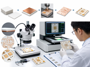
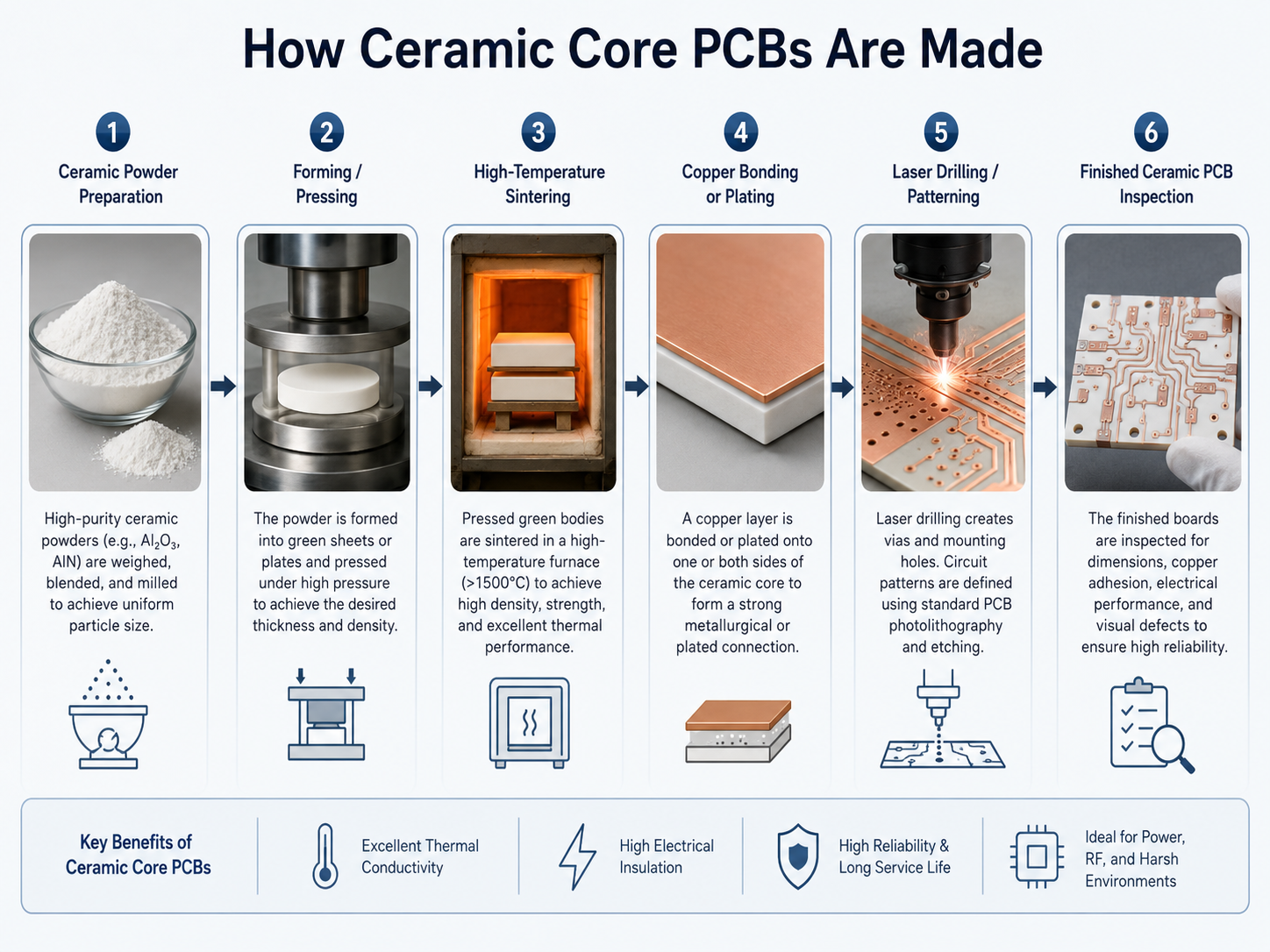
Ceramic cores are made through a controlled process that starts with ceramic powder preparation and ends with a dense, stable substrate suitable for circuit formation. The exact process depends on the material and final PCB structure.

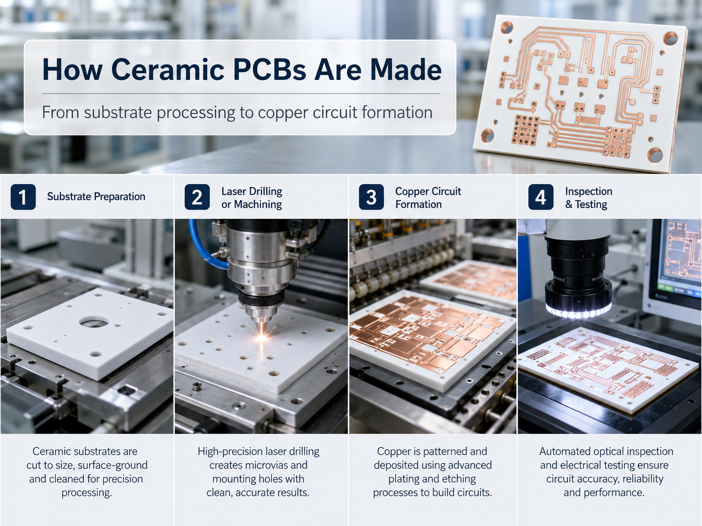
In a typical ceramic substrate process, ceramic powder is mixed with binders and additives to form a workable material. The material is shaped into sheets or pressed forms, then dried and sintered at high temperature. Sintering gives the ceramic its hardness, density, and stable physical properties. After that, the substrate may be lapped, polished, laser drilled, metallized, plated, etched, and finished according to the PCB design.

For circuit formation, different ceramic PCB technologies can be used. DPC, or Direct Plated Copper, is often chosen for fine circuits and high-precision designs. DBC, or Direct Bonded Copper, bonds copper directly onto the ceramic surface and is often used for power modules. AMB, or Active Metal Brazing, provides very strong bonding and is suitable for high-reliability power electronics.

Process TypeMain FeatureTypical Application
DPC ceramic PCBUses copper plating technology for fine circuits and precision patternsLED modules, sensors, optical devices, high-density ceramic circuits
DBC ceramic PCBDirect copper bonding provides strong thermal and current capacityPower modules, IGBT substrates, high-power electronics
AMB ceramic PCBActive brazing creates strong copper-to-ceramic bondingAutomotive power modules, high-reliability energy electronics
Thick-film ceramic PCBConductive paste is printed and fired onto ceramicHeaters, sensors, hybrid circuits, industrial modules
Thin-film ceramic PCBHigh-precision metal layers are deposited on ceramicMicrowave circuits, precision sensors, RF electronics

A professional ceramic PCB manufacturer must control material quality, sintering conditions, copper adhesion, surface flatness, circuit accuracy, and inspection standards. EBest Circuit combines process knowledge with practical PCB engineering support, helping customers choose the right ceramic core manufacturing process for the final product environment.

What thermal performance does ceramic core PCB deliver?

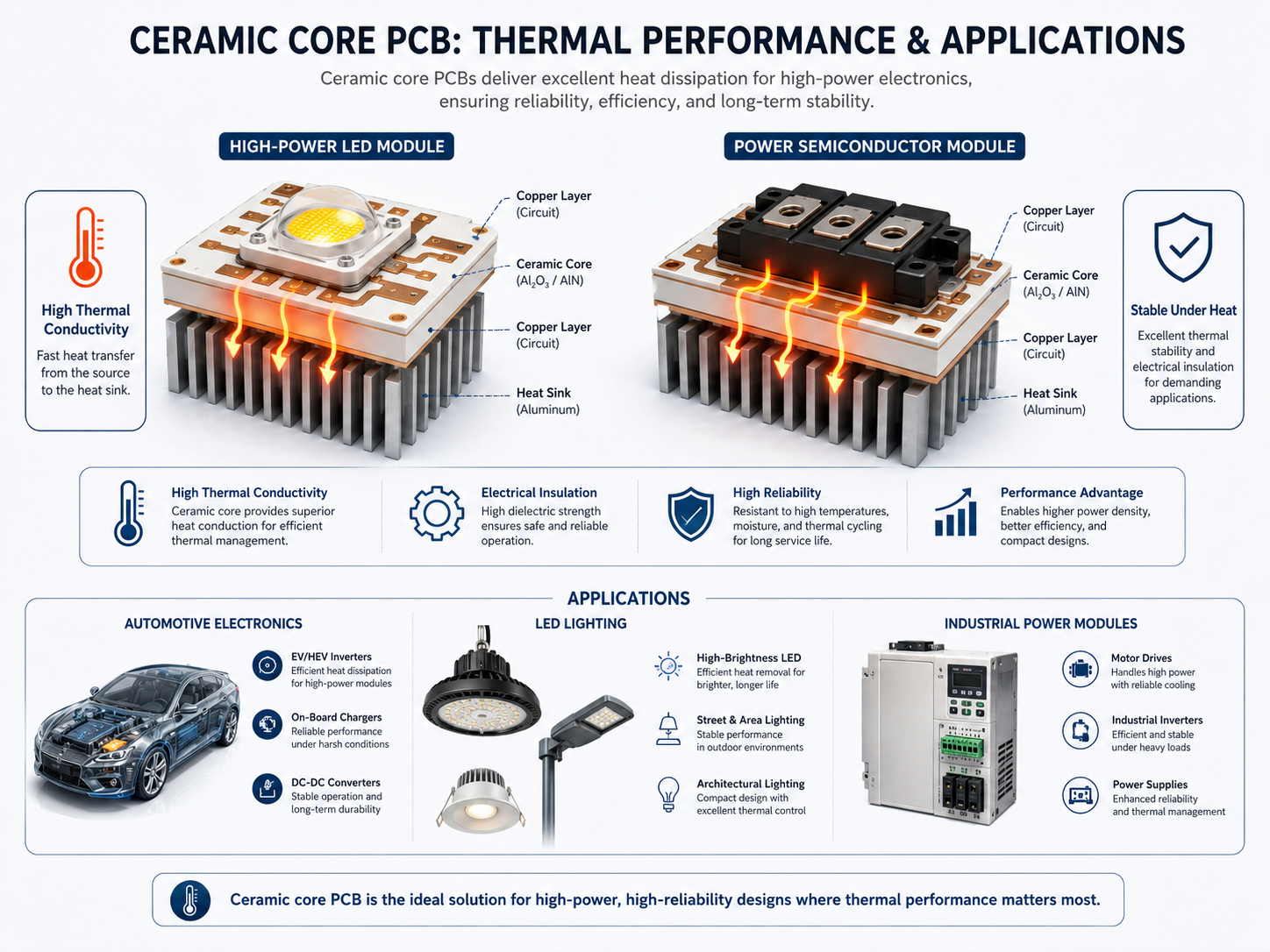
Ceramic core PCB delivers much stronger thermal performance than standard FR4 boards. The main advantage is that ceramic materials can transfer heat efficiently while still providing electrical insulation.

Alumina PCB offers good thermal conductivity for many industrial and LED applications. Aluminum nitride PCB provides a much higher level of heat transfer and is often used where thermal density is more demanding. With the right copper thickness, layout, and mounting structure, ceramic PCB boards can move heat away from components quickly and help maintain stable operating temperatures.

Thermal performance is not only about the ceramic material itself. The final result also depends on copper design, substrate thickness, dielectric path, via structure, solder joint quality, component placement, and heat sink contact.

MaterialGeneral Thermal PerformanceBest-Fit Applications
FR4Limited thermal conductivityGeneral electronics and low-to-medium power circuits
Alumina ceramicGood thermal conductivity with balanced costLEDs, sensors, industrial modules, moderate power electronics
Aluminum nitride ceramicExcellent thermal conductivityHigh-power LEDs, laser modules, power semiconductors, automotive electronics
Silicon nitride ceramicStrong thermal and mechanical reliabilityHigh-reliability power modules and harsh operating environments

For thermal-sensitive designs, EBest Circuit can support layout review and material comparison. This is helpful when customers need to decide between alumina PCB and aluminum nitride PCB, or when they want to optimize the balance between ceramic PCB cost, heat dissipation, and long-term reliability.

What are ceramic cores used for?

Ceramic cores are used in electronic products that need better thermal control, high insulation, stable structure, and reliable performance under demanding conditions. They are especially useful where compact size and high power must coexist. Because ceramic materials can transfer heat efficiently while maintaining electrical separation, they are widely used in modern power, lighting, automotive, medical, and communication systems.

In LED products, ceramic PCB helps move heat away from LED chips and supports stable brightness. In power electronics, ceramic substrates are used for modules that handle high current and high voltage. In RF and microwave circuits, ceramic materials can provide stable electrical characteristics. In medical and aerospace electronics, ceramic PCB boards support reliability, precision, and long service life.

  • High-power LED modules and lighting engines
  • Laser diode modules and optical devices
  • Power semiconductor packages and IGBT modules
  • Automotive electronics and electric vehicle power modules
  • RF, microwave, and communication circuits
  • Medical sensors and monitoring devices
  • Industrial control modules and high-temperature electronics
  • Aerospace, UAV, and high-reliability electronic assemblies

Ceramic core PCB is a strong choice when the product needs more than ordinary PCB performance. Alumina PCB is suitable for balanced thermal and cost requirements, while aluminum nitride PCB is ideal for stronger heat dissipation. For custom ceramic PCB boards, ceramic PCB materials, ceramic PCB cost evaluation, and ceramic core manufacturing process support, EBest Circuit (Best Technology) can help engineers build a practical path from prototype to production.

Summary:

Ceramic core PCB is not simply a premium version of FR4. It is a specialized circuit platform for products that need excellent heat transfer, high insulation, stable operation, and compact design. If your project requires alumina PCB, aluminum nitride PCB, or custom ceramic PCB manufacturing support, you can contact sales@bestpcbs.com for project discussion and quotation support.

You may also like

China Medical PCB Assembly, Medical PCB Assembly Services

May 7th, 2026

What sets medical PCB assembly apart from standard PCB assembly?

Medical PCB assembly is built around reliability, traceability, process discipline, and long-term performance. A standard consumer electronics board may be designed mainly for cost, speed, and everyday function. A PCB assembly medical device project, however, must support a more controlled use environment. The board may work inside patient monitoring equipment, diagnostic instruments, imaging systems, wearable health devices, infusion systems, dental equipment, laboratory analyzers, or portable medical electronics. In these applications, stable electrical behavior, clean soldering, correct component sourcing, and documented production records matter from the first prototype to the final shipment.

China Medical PCB Assembly, Medical PCB Assembly Services

The biggest difference is not only the board itself. It is the manufacturing mindset behind it. Medical PCB assemblies need tighter control over materials, soldering profiles, component approval, cleaning, inspection, packaging, and revision management. The manufacturer has to understand that a small change in a resistor brand, solder paste type, conformal coating, or cleaning method can influence performance, certification work, or future maintenance. That is why a qualified medical device PCB assembly manufacturer usually provides engineering review, DFM feedback, BOM checking, quality records, and full communication before mass production begins.

Medical electronics also require a more mature supply chain. A normal commercial PCB assembly may allow several component substitutions if the electrical value is the same. For medical device PCB assembly, alternates must be reviewed more carefully. Component lifecycle, traceability, compliance status, package consistency, and manufacturer authorization all become part of the decision. This is especially important for long-life medical products, where a device may remain in production, servicing, or field use for many years.

Comparison PointStandard PCB AssemblyMedical PCB Assembly
Main priorityCost, delivery, general functionReliability, consistency, documentation, and stable performance
Component sourcingApproved equivalents may be flexibleApproved vendor lists and traceable sourcing are strongly preferred
Process controlGeneral SMT and DIP process controlControlled assembly process with tighter inspection and records
TestingAOI, functional test, or sample testing depending on productAOI, X-ray, ICT, flying probe, functional test, burn-in, or custom testing based on device needs
DocumentationBasic production files and inspection reportBOM records, process logs, quality reports, batch traceability, and change control
Risk levelUsually lower in daily consumer useHigher because the board may support healthcare equipment
Supplier expectationBuild according to filesReview, suggest, verify, record, and support engineering decisions

For this reason, medical PCB assembly services should be selected with more care than ordinary electronics manufacturing. A good supplier does not only place components on a board. It helps customers improve manufacturability, reduce production variation, and prepare the project for stable scaling. EBest Circuit (Best Technology) supports this type of work through PCB fabrication, component sourcing, PCBA production, inspection, and engineering assistance for medical and other high-reliability electronics.

Which medical devices need custom PCB assembly?

Many medical devices need custom PCB assembly because their size, function, sensor interface, power requirement, safety requirement, and communication method are different from standard electronics. A medical monitoring PCB assembly for bedside equipment is not the same as a flexible board used in a wearable patch. A diagnostic analyzer may need stable signal acquisition, while a handheld device may need compact layout, battery management, and low-power operation. Customization allows the PCB and assembly process to match the exact device architecture.

Custom medical PCB assembly is often used when the device has unique mechanical constraints. For example, wearable health products may require thin rigid-flex boards to fit inside compact housings. Imaging modules may require high-density interconnect boards with controlled impedance. Laboratory instruments may need robust connectors, shielded areas, high-reliability solder joints, and stable thermal behavior. Portable medical products often need lightweight boards, fine-pitch components, and secure battery circuits.

Typical medical devices that need custom PCB assembly include:

  • Patient monitors, ECG devices, EEG systems, pulse oximeters, and blood pressure monitors
  • Diagnostic instruments, laboratory analyzers, medical imaging modules, and test equipment
  • Wearable health devices, smart patches, hearing-related electronics, and portable therapy devices
  • Infusion pumps, respiratory devices, dental equipment, endoscopy accessories, and rehabilitation systems
  • Medical communication modules, sensor boards, control boards, power boards, and human-machine interface boards

The design style also changes by application. A wearable device may focus on compact size, low weight, and soft interconnection. A hospital instrument may focus on stable operation, easy servicing, and strong connector retention. A diagnostic module may need excellent signal integrity, low noise, and repeatable calibration behavior. This is why custom medical device PCB assembly should be reviewed from both engineering and manufacturing perspectives.

EBest Circuit (Best Technology) can support different forms of PCB assembly for medical applications, including rigid PCB assembly, rigid-flex PCB assembly, HDI board assembly, high-frequency board assembly, and turnkey assembly.

For customers looking for the best rigid-flex PCB assembly services for medical devices, supplier experience in lamination control, flexible material handling, assembly fixture design, and final testing is especially valuable. Rigid-flex boards can reduce cable use and save space, but they require experienced process control during fabrication and assembly.

What standards does medical PCB assembly have to follow?

Medical PCB assembly has to follow product requirements, customer requirements, quality system requirements, and market compliance requirements. The exact standards depend on the medical device type, the region where the device will be sold, and the role of the PCB assembly in the final product. A PCB supplier may not certify the complete medical device, but the assembly process should support the customer’s regulatory pathway with stable manufacturing records and controlled production practices.

ISO 13485 is one of the most recognized quality management standards for medical device manufacturing. It focuses on quality control, risk management, documentation, traceability, and consistent production practices. For PCB assembly medical device projects, working with a supplier familiar with ISO 13485 expectations helps improve communication and documentation discipline. ISO 9001 is also commonly used as a baseline quality management system for electronics manufacturing.

IPC standards are also widely used in PCB and PCBA production. IPC-A-610 provides acceptability criteria for electronic assemblies, and many high-reliability boards are built to Class 2 or Class 3 requirements depending on use conditions. IPC-J-STD-001 is often referenced for soldered electrical and electronic assemblies. For bare PCB fabrication, IPC-6012, IPC-6013, and related documents may apply depending on whether the design is rigid, flexible, or rigid-flex. These standards help align expectations for workmanship, solder quality, board acceptance, and inspection.

Medical products may also need to consider electrical safety, electromagnetic compatibility, risk management, and material compliance. IEC 60601-1 is often associated with medical electrical equipment safety. IEC 60601-1-2 relates to EMC requirements for medical electrical equipment. ISO 14971 is commonly used for medical device risk management. RoHS and REACH may apply for material compliance in many markets. The PCB assembly manufacturer should understand how its production records, material control, and change management support the customer’s larger compliance work.

Standard or Requirement AreaWhy It Matters in Medical PCB Assembly
ISO 13485Supports medical device quality management, documentation, traceability, and process discipline
ISO 9001Provides a general quality management foundation for manufacturing control
IPC-A-610Defines acceptance criteria for electronic assemblies and solder workmanship
IPC-J-STD-001Guides soldering process requirements for reliable electronic assemblies
IEC 60601-related requirementsSupports safety and EMC expectations for many medical electrical devices
ISO 14971Helps customers manage risk across the medical device lifecycle
RoHS and REACHSupport material compliance for regulated markets
UL, when requiredHelps with recognized materials, safety-related component choices, and product market entry

For practical production, standards are only useful when they are translated into daily action. This means controlled incoming inspection, correct storage of moisture-sensitive devices, calibrated equipment, approved solder profiles, first article inspection, AOI programming, X-ray checking for hidden joints, test fixture validation, and controlled release of finished assemblies. EBest Circuit (Best Technology) integrates these manufacturing controls into its PCB and PCBA services so customers can move from prototype to production with clearer process visibility.

China Medical PCB Assembly, Medical PCB Assembly Services

Is automated assembly better for medical PCBs?

Automated assembly is usually the better choice for most medical PCBs because it gives more repeatable placement accuracy, controlled solder paste printing, stable reflow profiles, and efficient inspection. Medical PCB assembly automation is especially valuable when the board includes fine-pitch ICs, BGAs, small passive components, dense layouts, or high-volume production. Automation helps the manufacturer keep each board close to the same process condition, which is very important for repeatability.

However, automation does not replace engineering judgment. A fully automated SMT line still needs correct stencil design, solder paste selection, feeder setup, component verification, reflow profiling, AOI programming, and quality review. For some medical PCB assemblies, manual work may still be needed for through-hole connectors, wires, shields, mechanical parts, conformal coating, selective soldering, or final device-level integration. The right answer is often a balanced process: use automation where it improves consistency, and use trained manual operations where controlled human work gives better results.

Assembly MethodBest Use CaseStrength for Medical PCBsConsideration
Automated SMT assemblyFine-pitch components, dense layouts, medium to high volumeHigh repeatability, fast placement, stable process controlRequires accurate programming, proper stencil design, and verified materials
Manual assemblyLow-volume builds, special connectors, wires, hand-fit partsFlexible and useful for complex mechanical stepsRequires skilled operators, work instructions, and careful inspection
Selective solderingThrough-hole parts on mixed-technology boardsConsistent soldering for connectors and larger partsFixture design and thermal profile control are important
Automated optical inspectionPost-placement and post-reflow checkingQuickly detects polarity, missing parts, offset, and solder defectsNeeds proper programming and inspection standards
X-ray inspectionBGA, QFN, hidden solder jointsHelps verify solder quality under packagesOften used based on package type and product risk
Functional testingFinal board behavior verificationConfirms the board performs as intendedTest coverage depends on fixture design and customer requirements

For prototypes, automation can also be useful because it helps early builds reflect future production conditions. A quick turn medical PCB assembly project may start with a small batch, but if the long-term plan includes production, building early samples with scalable methods makes the transition smoother. The manufacturer can identify stencil issues, placement constraints, component packaging concerns, and test access problems before the design is released.

EBest Circuit (Best Technology) supports medical PCB assembly automation with SMT production, inspection, testing, and engineering review. The goal is not just fast assembly. The stronger goal is controlled assembly. When the same process logic is used from prototype through pilot run and mass production, customers can gain clearer feedback and better confidence in the final build.

What does turnkey medical PCB assembly include?

Turnkey medical PCB assembly means the manufacturer supports more than component placement. It usually includes PCB fabrication, component sourcing, incoming material inspection, SMT assembly, through-hole assembly, cleaning, inspection, testing, packaging, and delivery. In many projects, turnkey service also includes DFM review, BOM optimization, engineering communication, and documentation support. This approach saves time for medical device companies because they do not need to coordinate separate PCB factories, component suppliers, and assembly houses.

A medical PCB assembly turnkey service is especially helpful when the customer wants one accountable partner. If a bare board issue, component issue, or assembly issue appears, the turnkey supplier can review the complete production chain more quickly. This reduces communication gaps and helps engineers solve problems with a complete view of the project. For medical device PCB assembly, this integrated model is often more practical than separating each manufacturing step.

Turnkey service can include:

  • PCB fabrication for rigid, flexible, rigid-flex, HDI, high-frequency, ceramic, or metal-core designs
  • Component sourcing through approved channels, BOM review, lifecycle checks, and alternative suggestions
  • SMT assembly, through-hole assembly, selective soldering, conformal coating, cleaning, and final inspection
  • AOI, X-ray, ICT, flying probe, functional testing, burn-in, and customized test fixture support
  • Quality documents, production records, traceability files, packing control, and logistics support

The value of turnkey service is strongest when it starts early. Before production, the supplier can check land patterns, component spacing, solder mask openings, fiducials, panel design, test points, impedance requirements, thermal design, connector position, and assembly clearance. These details may look small, but they can influence yield, test coverage, and production stability. Early review gives the customer a better chance to correct issues before the first batch.

EBest Circuit (Best Technology) offers turnkey support for PCB assembly for medical and other high-reliability applications. The company can combine PCB fabrication, component procurement, PCBA assembly, testing, and engineering support into one service flow. For customers developing medical device PCB assembly projects, this can simplify sourcing, shorten communication loops, and provide more consistent records from bare board to finished assembly.

Can I get quick turn medical PCB assembly for prototypes?

Yes, quick turn medical PCB assembly is possible for prototypes, pilot runs, and engineering validation builds. The practical delivery time depends on PCB complexity, material availability, component lead time, surface finish, layer count, assembly density, inspection needs, and test requirements. A simple 2-layer or 4-layer prototype with available components can move quickly. A rigid-flex, HDI, controlled impedance, or high-frequency medical board may need more review and process preparation.

Quick turn does not mean careless work. For medical PCB assemblies, fast delivery should still include DFM checking, BOM verification, material confirmation, SMT preparation, inspection, and basic quality records. The best prototype service balances speed with discipline. A rushed build that skips review may create confusion later. A well-managed quick turn build helps engineers test form, fit, function, firmware, signal behavior, power performance, and assembly feasibility in a useful timeline.

To improve prototype speed, customers can prepare complete and clear files. Gerber or ODB++ data, drill files, pick-and-place files, BOM with manufacturer part numbers, assembly drawings, polarity markings, test instructions, impedance notes, and special process requirements should be shared together. If alternates are acceptable, the customer should define the approval rules in advance. This helps the assembly team quote faster and avoid repeated questions.

Quick turn is also valuable for design iteration. Medical device development often moves through several rounds of prototypes before production approval. Each round may test a different housing, sensor position, connector orientation, battery layout, firmware version, or mechanical fit. When the PCB assembly manufacturer can respond quickly and provide feedback, the customer can improve the design with more confidence.

EBest Circuit (Best Technology) supports quick turn medical PCB assembly for prototype and small-batch needs, depending on project complexity and material readiness. The company’s engineering team can review files before production and suggest improvements for manufacturability. This is helpful for startups, medical equipment developers, and engineering teams that need practical feedback before investing in larger production quantities.

Why choose China manufacturers for medical PCB assembly?

China medical PCB assembly is attractive to many global companies because China has a mature electronics manufacturing ecosystem. Customers can access PCB fabrication, component sourcing, SMT assembly, tooling, testing, cable assembly, enclosure integration, and logistics support in one supply chain region. For medical electronics, this can create practical advantages in speed, engineering response, supplier coordination, and cost control.

The strongest China manufacturers are no longer simple low-cost assembly vendors. Many have invested in automated SMT lines, AOI, X-ray inspection, clean production areas, traceability systems, quality management, and engineering teams. For Western technical teams, the real value is not only price. It is the ability to support prototype, pilot production, design improvement, and scalable manufacturing under one roof.

China manufacturers can also be useful for custom medical PCB assembly because many projects need varied processes. A medical device may require a rigid-flex PCB, fine-pitch BGA assembly, precision connector soldering, conformal coating, functional testing, and controlled packaging. A supplier with broad in-house capability can coordinate these steps more smoothly. This is especially helpful when the project has frequent engineering changes during development.

At the same time, customers should choose carefully. A medical PCB assembly manufacturer should be evaluated by quality system, engineering skill, process capability, traceability, communication, inspection equipment, and willingness to support documentation. The lowest quote is not always the best long-term choice. The better supplier is the one that helps the project become stable, repeatable, and easier to manage.

EBest Circuit (Best Technology) is a China-based PCB and PCBA manufacturer with experience in medical, industrial, automotive, communications, and high-reliability electronics. The company supports PCB fabrication, component sourcing, assembly, inspection, and testing. For customers looking for a medical device PCB assembly manufacturer in China, EBest Circuit (Best Technology) can provide engineering support and turnkey production services that help bridge prototype development and reliable manufacturing.

How does the medical PCB assembly process work step by step?

The medical PCB assembly process works best when it follows a controlled, documented, and reviewable path. The process starts before production. Engineering files are checked, the BOM is reviewed, materials are confirmed, and the assembly method is planned. This early stage is important because it prevents many common production issues and helps the customer understand cost, timeline, and manufacturability.

After file review, the bare PCB is fabricated or prepared for assembly. The manufacturer checks board quality, surface finish, solder mask, copper features, hole quality, and panel format. For rigid-flex or HDI designs, fabrication control is especially important because the board structure itself may be more complex. Once bare boards and components are ready, incoming inspection confirms that materials match the approved build requirements.

SMT assembly then begins with solder paste printing. A stencil is used to apply solder paste to the pads. The boards pass through solder paste inspection when required, then components are placed by automated equipment. After placement, the boards move through reflow soldering under a controlled thermal profile. The reflow profile must match solder paste, board material, component sensitivity, and thermal mass. After reflow, AOI checks component position, polarity, missing parts, solder bridges, and visible solder quality.

If the board uses BGAs, QFNs, or hidden solder joints, X-ray inspection may be used. Through-hole parts may be soldered manually, by wave soldering, or by selective soldering. Cleaning, conformal coating, programming, calibration, and mechanical assembly may follow depending on the design. Finally, the board is tested through ICT, flying probe, functional test, or a customer-defined test fixture.

A typical step-by-step flow looks like this:

  1. Engineering file review, DFM analysis, BOM checking, and quotation confirmation.
  2. PCB fabrication, component sourcing, and incoming quality inspection.
  3. Stencil preparation, solder paste printing, and solder paste inspection when required.
  4. SMT component placement, reflow soldering, and AOI inspection.
  5. X-ray inspection for hidden solder joints such as BGA, QFN, and LGA packages.
  6. Through-hole assembly, selective soldering, manual soldering, or mechanical assembly.
  7. Cleaning, conformal coating, firmware programming, calibration, and labeling if required.
  8. ICT, flying probe, functional test, burn-in, final inspection, packing, and shipment.

The process may change based on the product. A medical monitoring PCB assembly may require sensor calibration and functional test. A portable device may require battery charging test, communication test, and power consumption measurement. A diagnostic instrument board may need signal verification, connector inspection, and long-duration operation testing. The assembly process should always match the device function and risk profile.

EBest Circuit (Best Technology) can support this workflow from early DFM review to finished PCBA delivery. For customers using turnkey medical PCB assembly services, the company can help coordinate PCB fabrication, component sourcing, SMT assembly, inspection, and testing in one manufacturing chain.

China Medical PCB Assembly, Medical PCB Assembly Services

What are the benefits of custom medical device PCB assembly?

Custom medical device PCB assembly gives engineers more control over size, function, performance, and product integration. Medical products often need a board that fits a unique enclosure, works with selected sensors, supports specific communication interfaces, and meets defined test requirements. A custom board allows the design team to optimize these details instead of forcing the product around an off-the-shelf solution.

Another benefit is better electrical performance. Medical electronics may process small signals from sensors, electrodes, optical modules, pressure devices, or analog front ends. Custom PCB layout can improve signal routing, grounding, shielding, impedance control, and noise behavior. Power design can also be tailored for battery life, charging safety, isolation, heat control, and stable voltage regulation.

Custom assembly also helps with mechanical integration. A rigid-flex PCB can replace cables and connectors in compact medical devices. HDI technology can support dense components in smaller spaces. Metal-core or thermal design methods can help with heat dissipation in power-related medical equipment. Surface finish, coating, connector type, and board thickness can be selected based on device use conditions.

From a business viewpoint, custom PCB assembly supports better product identity and long-term control. The customer can define the approved BOM, firmware interface, test method, production records, and revision plan. This makes future production easier to manage. It also helps when a product must be serviced, updated, or transferred into larger production.

For medical device developers, the main benefits include improved fit, better performance, stronger production control, and more flexible engineering options. A custom build can be shaped around the product rather than the other way around. When paired with a qualified supplier, it becomes easier to refine the design, verify the process, and prepare the product for stable manufacturing.

EBest Circuit (Best Technology) supports custom medical PCB assembly for customers who need more than a standard build. The company can assist with material selection, stack-up review, DFM suggestions, PCB fabrication, component sourcing, and assembly testing. This makes it suitable for projects such as patient monitors, diagnostic equipment, wearable health electronics, laboratory modules, and other medical electronics that need reliable board-level manufacturing.

How to pick a qualified medical PCB assembly manufacturer?

Picking a qualified medical PCB assembly manufacturer should start with process capability and quality mindset. The supplier should understand that medical electronics need stable manufacturing, clear documentation, and careful communication. A good manufacturer will ask questions before production, review files carefully, and explain concerns in a practical way. This is far better than simply accepting files and building boards without engineering feedback.

The first area to check is quality management. Ask whether the supplier has ISO 9001, ISO 13485 experience or certification, IPC workmanship standards, traceability systems, incoming inspection, equipment calibration, and process records. Also ask how they manage engineering changes, material substitutions, nonconforming products, and production feedback. These answers show whether the supplier can support long-term medical device PCB assembly or only one-time sample builds.

The second area is technical capability. Review whether the manufacturer can handle the board type, component package, assembly density, testing method, and coating requirement. If your project uses BGA, QFN, 01005 components, rigid-flex PCB, HDI structure, controlled impedance, high-frequency materials, or special connectors, the supplier should show real production experience. For medical PCB assembly services, experience is often more important than a long equipment list.

The third area is sourcing strength. Medical products need stable components and traceable supply. A qualified supplier should help review manufacturer part numbers, lifecycle status, packaging, date code, compliance, and available alternates. For turnkey assembly, component sourcing quality can influence the entire project. Good sourcing also helps quick turn medical PCB assembly because material readiness often decides the real delivery time.

Communication is also very important. Western technical teams usually need clear English communication, fast engineering response, organized quotations, and practical production feedback. A strong supplier will point out unclear drawings, missing polarity marks, risky component spacing, weak test access, or possible soldering issues before the build. This kind of feedback saves time and improves confidence.

EBest Circuit (Best Technology) is a suitable partner for customers looking for China medical PCB assembly, custom medical PCB assembly, and medical PCB assembly turnkey service. The company combines PCB fabrication, component procurement, PCB assembly, inspection, testing, and engineering support. Its experience with rigid, rigid-flex, HDI, high-frequency, ceramic, metal-core, and other PCB technologies gives customers more options for different medical device designs.

China Medical PCB Assembly, Medical PCB Assembly Services

In brief, medical PCB assembly is different because it requires stronger process control, careful sourcing, detailed inspection, and clear production records. The right supplier should support the product from prototype to stable production while helping engineers improve manufacturability and reliability. For medical PCB assembly services, medical monitoring PCB assembly, quick turn medical PCB assembly, or turnkey PCBA support, you can contact EBest Circuit (Best Technology) at sales@bestpcbs.com

You may also like

China IC Board Design Manufacturer, Factory Price IC Board Design

April 24th, 2026

Integrated circuits sit quietly at the heart of modern electronics, yet the work behind their design and integration onto boards is anything but simple. Whether you are developing industrial control systems, consumer electronics, or communication devices, a well-executed IC board design directly shapes performance, reliability, and production cost. Many engineers and sourcing professionals are now turning to China IC board design manufacturers for a practical balance between engineering expertise and factory pricing, especially when speed and scalability matter.

China IC Board Design Manufacturer, Factory Price IC Board Design

What is IC design?

IC design refers to the process of creating integrated circuits, where multiple electronic components such as transistors, resistors, and capacitors are fabricated onto a single semiconductor substrate. Instead of assembling discrete components on a board, IC design compresses entire functional systems into compact silicon chips.

From a practical standpoint, IC design involves several stages:

  • Concept and functional specification
  • Circuit schematic development
  • Simulation and verification
  • Layout design at the semiconductor level
  • Fabrication and testing

Unlike traditional board-level design, IC design operates at a microscopic scale. Engineers deal with nanometer-level geometries, signal integrity inside silicon, and power distribution within extremely tight constraints. This level of integration allows devices to achieve high performance while maintaining low power consumption and compact size.

In real-world applications, IC design enables:

  • Microcontrollers used in industrial automation
  • Communication chips in wireless devices
  • Power management ICs in automotive systems
  • Sensor ICs in medical and wearable equipment

Is IC design the same as PCB design?

IC design and PCB design are closely related, yet fundamentally different disciplines. They operate at different levels of abstraction, use different tools, and address distinct engineering challenges.

IC design focuses on what happens inside the chip, while PCB design determines how that chip interacts with other components on a board. Both are essential, but they require different skill sets and design methodologies.

Here is a clear comparison:

AspectIC DesignPCB Design
Design LevelSemiconductor (chip-level)Board-level (system integration)
ScaleNanometer to micrometerMillimeter to centimeter
ComponentsTransistors, diodes, passive elementsICs, connectors, discrete components
ToolsEDA tools for chip layoutPCB CAD tools (Altium, Eagle, etc.)
FocusFunctionality within siliconConnectivity and physical layout
ManufacturingSemiconductor fabrication plantsPCB fabrication and assembly

While IC design defines the internal behavior of a chip, PCB design ensures that the chip functions correctly within a larger system. A mismatch between these two layers can lead to signal issues, power instability, or thermal challenges.

Professional IC board design combines both perspectives. Companies like EBest Circuit (Best Technology) approach this by aligning chip specifications with PCB layout strategies, ensuring that every IC performs optimally once mounted on the board.

China IC Board Design Manufacturer, Factory Price IC Board Design

How Do You Identify IC on PCB?

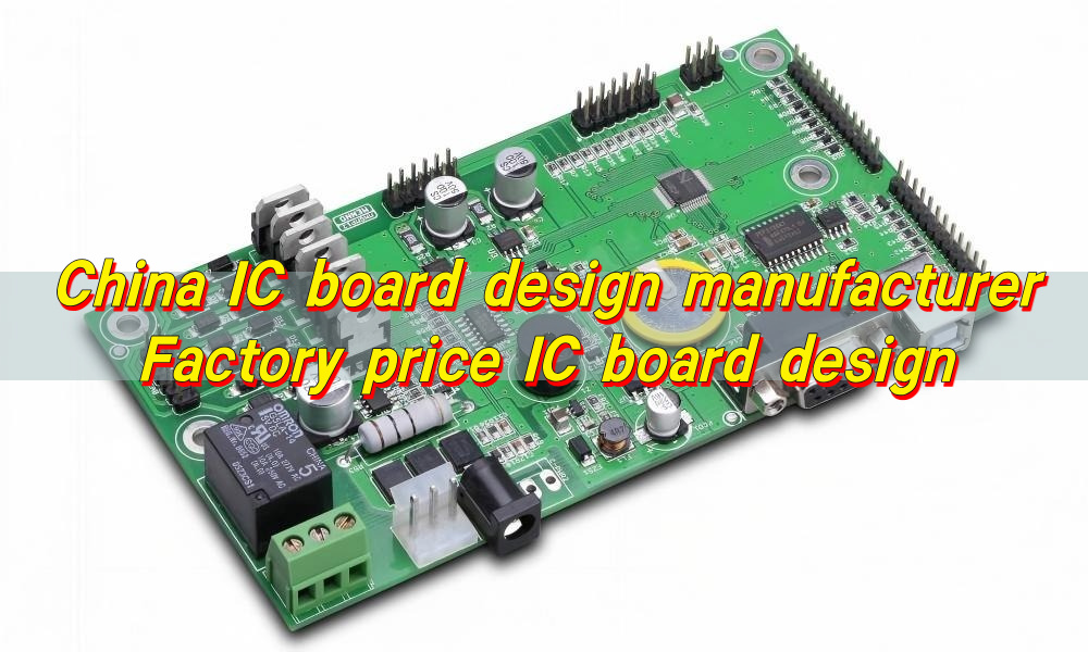
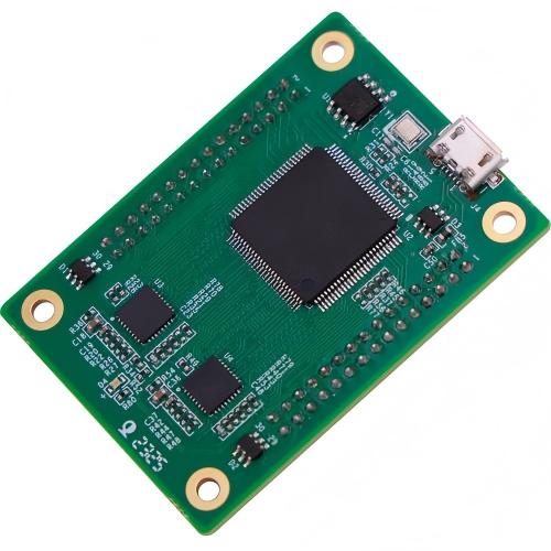
ICs are typically the most functionally significant components on a board, and they often have distinctive physical and labeling characteristics.

On a typical PCB, ICs can be recognized by:

  • Black or dark-colored rectangular packages
  • Multiple pins arranged in rows or grids
  • Markings such as part numbers, manufacturer codes, or logos
  • Placement near key functional zones like processing, communication, or power regulation

Different package types also provide clues:

  • DIP (Dual In-line Package): Larger, through-hole components often used in older or prototyping designs
  • SOP/SOIC: Surface-mounted packages with gull-wing leads
  • QFP (Quad Flat Package): Fine-pitch pins on all four sides
  • BGA (Ball Grid Array): No visible pins, solder balls underneath

To accurately identify an IC, engineers often rely on:

  • Silkscreen labels on the PCB (e.g., U1, U2)
  • Datasheets referenced by part numbers
  • Circuit schematics

In high-density IC board design, especially in industrial or compact consumer products, IC placement becomes more strategic. Proper identification supports troubleshooting, maintenance, and reverse engineering, making it a critical skill for engineers and technicians alike.

Is IC design hard?

IC design is widely regarded as one of the more demanding fields in electronics engineering, primarily due to its precision requirements and multi-layered complexity. With the right tools, structured workflows, and experienced teams, it becomes a highly manageable and rewarding process.

Several factors contribute to its complexity:

  • Extremely small geometries requiring precision design rules
  • Sensitivity to noise, interference, and power variations
  • Advanced simulation and verification requirements
  • High cost of fabrication errors

That said, modern design environments have significantly improved efficiency. Simulation tools can predict performance before fabrication, while standardized design libraries reduce repetitive work.

From a business perspective, partnering with a China IC board design manufacturer can simplify the process. Experienced teams handle layout optimization, signal integrity, and manufacturability, allowing clients to focus on product functionality and market strategy.

What is the IC design rule?

IC design rules are a set of constraints that guide how circuits are physically implemented on a semiconductor. These rules ensure that the design can be reliably manufactured and will function as intended under real-world conditions.

They are typically defined by semiconductor fabrication processes and include parameters such as:

  • Minimum spacing between components
  • Layer alignment tolerances
  • Maximum current density
  • Thermal distribution requirements

At the board level, IC board design also follows PCB-related rules to ensure compatibility between the chip and the board.

Key IC design rule categories include:

  • Geometric rules: Define minimum widths and spacing
  • Electrical rules: Ensure signal integrity and prevent interference
  • Thermal rules: Manage heat dissipation
  • Manufacturing rules: Align with fabrication capabilities

Design rule checking (DRC) tools automatically verify compliance before production. This step is essential because even a small violation can lead to failure during fabrication or operation.

For manufacturers offering factory price IC board design, strict adherence to design rules ensures consistent quality while keeping production efficient and cost-effective.

China IC Board Design Manufacturer, Factory Price IC Board Design

What key factors affect professional IC board design?

A high-quality IC board design is not just about placing components correctly. It involves a careful balance of electrical performance, mechanical stability, and manufacturability. Several key factors play a decisive role in achieving a professional result.

  • Signal integrity: High-speed signals require controlled impedance, proper routing, and minimized interference
  • Power distribution: Stable voltage delivery is essential for IC performance
  • Thermal management: Heat must be effectively dissipated to maintain reliability
  • Component placement: Strategic layout reduces noise and improves efficiency
  • Material selection: The choice of substrate influences durability and performance
  • Manufacturing compatibility: Design must align with fabrication and assembly processes

Additionally, modern IC board design often integrates advanced considerations such as electromagnetic compatibility (EMC) and miniaturization.

EBest Circuit (Best Technology), with its experience in PCB manufacturing and assembly, emphasizes these factors by offering a complete design-to-production workflow.

What are the 4 types of integrated circuits?

Integrated circuits can be broadly categorized into four main types, each serving distinct functional roles in electronic systems.

  • Analog ICs:
    These process continuous signals and are commonly used in amplification, filtering, and signal conditioning. Examples include operational amplifiers and voltage regulators.
  • Digital ICs:
    Designed for binary operations, digital ICs form the backbone of computing systems. Microprocessors, memory chips, and logic gates fall into this category.
  • Mixed-signal ICs:
    These combine analog and digital functionalities within a single chip. They are widely used in communication devices and data conversion systems.
  • Power ICs:
    Focused on energy management, power ICs regulate voltage, control power flow, and improve efficiency in systems such as power supplies and automotive electronics.

Each type plays a unique role in IC board design, and many modern devices integrate multiple types to achieve complex functionality.

Which is better IC or transistor?

The question of whether an IC or a transistor is “better” depends entirely on the application. A transistor is a single electronic component, while an IC is a collection of many components integrated into one package.

A concise comparison helps clarify:

FeatureTransistorIntegrated Circuit
ComplexitySingle componentMultiple components combined
FunctionalityLimitedHighly versatile
SizeLarger (when used in quantity)Compact integration
Cost EfficiencyHigher for complex systemsLower per function
ApplicationBasic switching/amplificationComplete system functions

In modern electronics, ICs are generally preferred because they offer higher functionality in a smaller footprint. However, discrete transistors are still valuable in specific scenarios, especially where customization or high-power handling is required.

In professional IC board design, both elements may coexist, but ICs dominate due to their efficiency and scalability.

China IC Board Design Manufacturer, Factory Price IC Board Design

What IC board material is suitable for industrial equipment?

Material selection is a critical decision in IC board design, particularly for industrial equipment where reliability and durability are essential. The environment often involves temperature fluctuations, mechanical stress, and electrical noise, all of which influence material choice.

Common materials include:

  • FR-4 (Flame Retardant Epoxy):
    The most widely used PCB material, offering a strong balance of cost, durability, and electrical performance
  • High-Tg FR-4:
    Enhanced thermal resistance, suitable for higher operating temperatures
  • Polyimide:
    Excellent thermal stability and flexibility, often used in demanding environments
  • Ceramic substrates:
    Superior thermal conductivity and electrical insulation, ideal for high-power applications
  • Metal-core PCBs:
    Efficient heat dissipation, commonly used in power electronics and LED systems

For industrial IC boards, the choice often leans toward materials that provide:

  • Stable electrical performance under load
  • Resistance to heat and environmental stress
  • Long operational lifespan

Manufacturers like EBest Circuit (Best Technology) tailor material selection based on application requirements, ensuring that each board meets both performance and durability expectations.

Summary:

IC board design bridges the gap between semiconductor innovation and real-world electronic systems. From understanding the fundamentals of IC design to selecting the right materials for industrial applications, every step contributes to the final product’s performance and reliability.

For businesses seeking efficient, cost-effective solutions, working with an experienced China IC board design manufacturer offers clear advantages. With strong engineering capabilities and streamlined production, companies like EBest Circuit (Best Technology) deliver high-quality designs aligned with global standards.

If you are exploring reliable IC board design solutions or need support for your next project, feel free to connect with us at: sales@bestpcbs.com

You may also like

High Thermal MCPCB Automotive: 2.0–5.0 W/m・K Solutions

April 16th, 2026

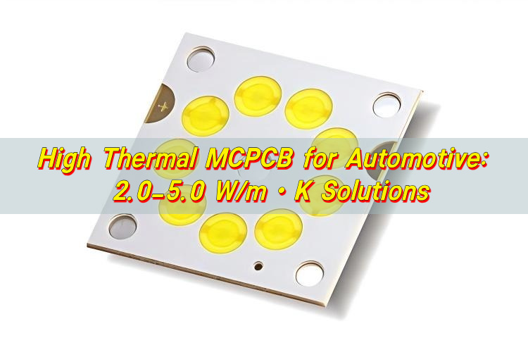
EBest’s High Thermal MCPCB Automotive delivers industry-leading thermal conductivity (2.0-3.0 W/m.K), IATF 16949, and other automotive-grade certifications, as well as reliable performance in extreme automotive environments (from -40°C to 150°C). Trusted for over 19 years, we solve your automotive thermal management challenges with turnkey solutions.

High Thermal MCPCB Automotive: 2.0–5.0 W/m・K Solutions

Why Choose EBest for Your High Thermal MCPCB Automotive Needs?

Our High Thermal MCPCB Automotive products are engineered to meet the toughest demands of automotive electronics, with core parameters that outperform industry standards—perfect for ECU, BMS, and ADAS modules.

Core parameters for High Thermal MCPCB Automotive: thermal conductivity up to 3.0 W/m.K, a maximum of 10 layers, thickness ranging from 12-157 mil, ±3 mil hole position tolerance, and a 94V-0 flammability rating. Partner with EBest today for your automotive MCPCB needs.

Why Choose EBest for High Thermal MCPCB Automotive?

  • Quality: 100% full inspection before delivery, automotive-grade materials, and strict compliance with all relevant certifications to ensure long-term reliability in harsh automotive conditions.
  • Lead Time: Urgent orders are shipped within 24 hours, regular orders are delivered on time, and our monthly capacity of 260,000 square feet allows us to handle any order size.
  • Service: One-stop solutions from design support to prototyping, production, and post-delivery support—we work with you to optimize your High Thermal MCPCB Automotive design for manufacturability.
  • Supply Chain: A stable, global supply chain for all electronic components (SMD, BGA, QFN, QFP) eliminates delays and ensures consistent product quality.

What Are the Key Pain Points of High Thermal MCPCB Automotive?

Many face challenges with thermal management failures, inconsistent quality, and supply chain disruptions when sourcing High Thermal MCPCB Automotive products—EBest addresses these head-on with proven solutions.

  • Thermal Failure: Our high thermal conductivity (2.0-3.0 W/m.K) and optimized PCB layout reduce hotspots by up to 25%, preventing component overheating in engine bays and other high-temperature areas.
  • Quality Inconsistency: We implement full-process quality control, from material selection to final inspection, ensuring every High Thermal MCPCB Automotive meets the same strict standards.
  • Supply Chain Risks: Our established global supply chain and in-house component sourcing eliminate delays, even for hard-to-find automotive-grade components.
  • Design Challenges: Our engineering team provides free design support to optimize your High Thermal MCPCB Automotive for thermal performance, signal integrity, and manufacturability.

For reliable, high-performance High Thermal MCPCB Automotive solutions that solve your biggest pain points, choose EBest—your trusted partner for automotive electronics.

What Is High Thermal MCPCB Automotive, and Why Is It Critical for Modern Cars?

High Thermal MCPCB Automotive is a metal-core printed circuit board designed specifically for automotive applications, with enhanced thermal conductivity to dissipate heat from high-power components.

Modern cars—especially electric vehicles (EVs)—rely on high-power electronics (ECU, BMS, ADAS, infotainment) that generate significant heat. Without effective thermal management, these components fail faster, risking safety and performance.

EBest’s High Thermal MCPCB Automotive efficiently transfers heat away from critical components, extending their lifespan and ensuring consistent performance in extreme automotive environments.

High Thermal MCPCB Automotive: 2.0–5.0 W/m・K Solutions

How Does High Thermal MCPCB Automotive Improve Automotive Electronics Reliability?

High Thermal MCPCB Automotive improves reliability by reducing thermal stress on components, which is the leading cause of failure in automotive electronics.

Our MCPCBs feature thermal conductivity up to 3.0 W/m.K—far higher than standard MCPCBs (0.8-1.0 W/m.K)—ensuring heat is quickly dissipated, even in tight engine bay spaces.

Additionally, our strict quality control and automotive-grade materials ensure the MCPCBs resist vibration, temperature cycles, and chemical exposure common in automotive settings.

What Thermal Conductivity Do You Need for High Thermal MCPCB Automotive?

The ideal thermal conductivity for High Thermal MCPCB Automotive depends on the application, but 2.0-3.0 W/m.K is the sweet spot for most automotive electronics.

For high-power components like EV BMS modules or ADAS processors, 3.0 W/m.K is recommended to handle peak heat generation. For less demanding applications (infotainment), 2.0 W/m.K is sufficient.

EBest offers customizable thermal conductivity options for High Thermal MCPCB Automotive, ensuring you get the exact performance your application requires.

How to Design High Thermal MCPCB Automotive for Maximum Thermal Performance?

To maximize thermal performance, focus on three key design elements: thermal conductivity, copper thickness, and component placement.

Choose a thermal conductivity of 2.0-3.0 W/m.K for automotive applications. Opt for thicker copper (up to 10 OZ) to improve heat transfer and reduce resistance.

Place high-power components near thermal vias or heat sinks, and avoid clustering components to prevent hotspots. EBest’s engineering team can help optimize your High Thermal MCPCB Automotive design for peak performance.

High Thermal MCPCB Automotive: 2.0–5.0 W/m・K Solutions

What Certifications Matter for High Thermal MCPCB Automotive?

Automotive-grade certifications ensure your High Thermal MCPCB Automotive meets strict industry standards for quality, safety, and reliability. EBest holds all critical certifications for automotive applications.

CertificationActual Value for High Thermal MCPCB Automotive
IATF 16949Ensures full-process control, from design to delivery, eliminating quality risks and meeting automotive industry quality standards.
ISO 9001:2015Guarantees consistent quality management systems, ensuring every High Thermal MCPCB Automotive meets the same high standards.
ISO 13485:2016Validates compliance for medical-grade automotive electronics (e.g., in-car health monitoring systems), ensuring safety and reliability.
AS9100DMeets aerospace-grade standards, ideal for high-reliability automotive applications like autonomous driving systems.
REACHEnsures no harmful substances are used, complying with EU automotive environmental regulations.
RoHSRestricts hazardous materials, making our High Thermal MCPCB Automotive environmentally friendly and compliant with global standards.
ULVerifies fire safety (94V-0 rating), critical for preventing thermal-related fires in automotive electronics.

What Services Does EBest Offer for High Thermal MCPCB Automotive?

EBest provides one-stop solutions for High Thermal MCPCB Automotive, covering every stage from design to delivery, with a focus on quality and efficiency.

Core Services for High Thermal MCPCB Automotive

  • PCB Fabrication: Custom High Thermal MCPCB Automotive prototypes and low-volume production, with customizable substrates and materials to match your needs.
  • Component Supply: Stable sourcing for all automotive-grade components (SMD, BGA, QFN, QFP) to ensure your MCPCBs are fully equipped and ready for assembly.
  • Assembly Services: BGA Assembly, Through-Hole Assembly, and Full Turnkey Assembly for High Thermal MCPCB Automotive, with 100% full inspection before delivery.

Value-Added Services

  • Injection Molding: Mold structure, thread insert, pad printing, and final assembly to integrate your High Thermal MCPCB Automotive into complete modules.
  • CNC Machining: Precision CNC Milling and Turning for tight tolerances, ideal for custom enclosures for High Thermal MCPCB Automotive.
  • Sheet Metal: Low-waste, flexible sheet metal solutions for heat sinks and enclosures, optimizing thermal performance for your MCPCBs.

How Does EBest’s High Thermal MCPCB Automotive Compare to Standard MCPCBs?

EBest’s High Thermal MCPCB Automotive outperforms standard MCPCBs in thermal performance, durability, and compliance—critical for automotive applications.

FeatureEBest High Thermal MCPCB AutomotiveStandard MCPCBs
Thermal Conductivity2.0-3.0 W/m.K (high thermal)0.8-1.0 W/m.K (standard)
CertificationsIATF 16949, ISO 13485, AS9100D, RoHS, ULBasic ISO 9001, limited automotive compliance
Temperature Resistance-40°C to 150°C (extreme automotive environments)0°C to 100°C (limited to mild environments)
Copper ThicknessUp to 10 OZ (14mil) for enhanced heat transfer1-2 OZ (3.5-7mil) standard
Quality Control100% full inspection, APQP, FMEA processesBasic inspection, no automotive-specific processes

What Are the Common Applications of High Thermal MCPCB Automotive?

High Thermal MCPCB Automotive is used in a wide range of automotive electronics, where thermal management is critical for performance and safety.

  • EV Battery Management Systems (BMS): Dissipates heat from high-power battery cells, ensuring battery safety and extending lifespan.
  • Engine Control Units (ECU): Handles heat from processing components in the engine bay, preventing overheating and performance issues.
  • ADAS (Advanced Driver Assistance Systems): Ensures reliable performance of cameras, sensors, and processors in all environmental conditions.
  • Infotainment Systems: Manages heat from high-power chips, ensuring smooth operation of touchscreens, audio systems, and connectivity features.
  • Lighting Systems: Dissipates heat from LED headlights and taillights, extending LED lifespan and maintaining brightness.

How Does EBest Ensure Consistent Quality for High Thermal MCPCB Automotive?

EBest prioritizes quality at every stage of production, ensuring your High Thermal MCPCB Automotive meets the strictest automotive standards.

  • Material Selection: We use A+ grade automotive materials, with strict supplier vetting to ensure consistency and durability.
  • Process Control: Fully automatic assembly lines and real-time quality monitoring prevent defects and ensure consistent performance.
  • Final Inspection: 100% full inspection before delivery, including thermal testing, electrical testing, and visual inspection.
  • Certifications: Compliance with IATF 16949 and other automotive certifications ensures our processes meet industry best practices.

What Is the Lead Time for EBest’s High Thermal MCPCB Automotive?

EBest offers flexible lead times for High Thermal MCPCB Automotive, designed to meet your project deadlines—even for urgent orders.

  • Prototypes: Ready for shipping within 24-48 hours for urgent requests, ensuring you can quickly test and validate your design.
  • Low-Volume Production: 3-5 business days, ideal for small-batch testing or initial production runs.
  • High-Volume Production: 7-10 business days, with our monthly capacity of 260,000 square feet to handle large orders without delays.

High Thermal MCPCB Automotive Case Study: Solving EV BMS Thermal Issues

A leading EV manufacturer struggled with BMS module overheating, which caused frequent shutdowns and reduced battery lifespan.

Their existing MCPCBs (1.0 W/m.K thermal conductivity) could not dissipate heat efficiently in the tight BMS enclosure, leading to component failure at 85°C.

EBest provided High Thermal MCPCB Automotive with 3.0 W/m.K thermal conductivity and an optimized copper layout. We also added thermal vias to improve heat transfer to the heat sink.

After implementation, the BMS module’s maximum temperature dropped to 68°C, eliminating shutdowns and extending battery lifespan by 20%. The manufacturer now uses EBest as their exclusive High Thermal MCPCB Automotive supplier.

High Thermal MCPCB Automotive: 2.0–5.0 W/m・K Solutions

FAQ: Common Questions About High Thermal MCPCB Automotive

  • Q1: What is the maximum layer count for EBest’s High Thermal MCPCB Automotive?

A1: The maximum layer count for our High Thermal MCPCB Automotive is 10 layers. This supports complex automotive electronics like ADAS and BMS modules, providing enough space for high-density components while maintaining thermal performance.

  • Q2: Can EBest customize High Thermal MCPCB Automotive for specific automotive applications?

A2: Yes, we offer full customization for High Thermal MCPCB Automotive. We can adjust thermal conductivity (2.0-3.0 W/m.K), board thickness (12-157 mil), copper thickness, and surface treatment to match your exact application needs.

  • Q3: Does High Thermal MCPCB Automotive work in extreme cold automotive environments?

A3: Yes, our High Thermal MCPCB Automotive is designed to perform reliably in extreme cold (-40°C) and hot (150°C) environments. This makes it ideal for all climates, from arctic regions to desert areas.

  • Q4: How do I know if my automotive application needs High Thermal MCPCB instead of standard MCPCB?

A4: If your application uses high-power components (e.g., BMS, ECU, ADAS) that generate significant heat, or if it’s installed in the engine bay or other high-temperature areas, you need High Thermal MCPCB Automotive. Standard MCPCBs will struggle to dissipate heat, leading to component failure.

  • Q5: Does EBest provide design support for High Thermal MCPCB Automotive?

A5: Yes, our engineering team offers free design support for High Thermal MCPCB Automotive. We help optimize your design for thermal performance, signal integrity, and manufacturability, ensuring your MCPCBs meet your application’s requirements.

  • Q6: What surface treatments are available for High Thermal MCPCB Automotive?

A6: We offer a range of surface treatments for High Thermal MCPCB Automotive, including ENIG, Flash Gold, Hard Gold Finger, Gold Plating, ENEPIG, ENIPIG, HAL, HASL(LF), OSP, Silver Immersion, and Tin Immersion—all compliant with automotive standards.

  • Q7: How does EBest’s supply chain ensure consistent delivery of High Thermal MCPCB Automotive?

A7: We have a stable, global supply chain for all materials and components needed for High Thermal MCPCB Automotive. Our purchasing team works with trusted suppliers, and we maintain inventory of key materials to avoid delays, even for urgent orders.

How to Order High Thermal MCPCB Automotive from EBest?

EBest provides high-performance High Thermal MCPCB Automotive solutions tailored to your automotive application. We offer urgent prototype delivery (within 24 hours), bulk order exclusive support, and free design assistance to ensure your project stays on track.

Don’t let thermal management issues or supply chain delays hold back your automotive project—contact us today to place your order. For urgent requests or custom quotes, email us at sales@bestpcbs.com. EBest: Your trusted partner for High Thermal MCPCB Automotive in 2026 and beyond.

You may also like

Circuit Board vs Motherboard: What’s the Difference?

January 27th, 2026

Circuit board vs motherboard is a common comparison, but the two terms are not interchangeable. A circuit board is the basic platform that holds and connects electronic components using copper traces. It is used in almost every electronic product, from simple controllers to complex industrial equipment.

Circuit Board vs Motherboard: What's the Difference?

What is a Circuit Board?

Circuit board is the physical platform that supports and connects electronic components. It provides mechanical stability, electrical pathways, and thermal management for an electronic system. Copper traces etched or printed onto an insulating base material form the conductive routes that allow current and signals to flow between components.

Circuit board is not a finished product by itself. It is a foundation. Components such as resistors, capacitors, integrated circuits, and connectors are mounted onto the board through surface-mount or through-hole methods. Once assembled, the board becomes a functional electronic unit.

In practical manufacturing terms, a PCB board serves several purposes at the same time. It ensures reliable electrical connections, keeps component placement organized, and improves consistency in mass production.

From consumer electronics to industrial automation, circuit boards are everywhere. You will find them inside power supplies, LED lighting, medical monitors, automotive controllers, and communication equipment.

At EBest Circuit (Best Technology), circuit boards range from basic two-layer boards to advanced HDI structures. Each design is tailored to its electrical load, signal speed, and operating environment.

What are the different types of circuit boards?

Circuit boards are not all built the same way. Their structure, material, and complexity vary based on application needs.

Common types of circuit boards include:

  • Single-layer circuit boards: These boards have copper on only one side. They are simple, low cost, and widely used in basic electronics such as toys, adapters, and simple control modules.
  • Double-layer circuit boards: Copper exists on both sides of the substrate. Vias connect the two layers. This design allows higher component density and more routing flexibility.
  • Multilayer circuit boards: These boards contain three or more copper layers stacked with insulating material in between. They support complex routing, controlled impedance, and stable power distribution.
  • Rigid circuit boards: Made from materials like FR-4, rigid boards hold their shape. They dominate most electronics applications.
  • Flexible circuit boards: Built on polyimide films, these boards bend and fold. They are common in cameras, wearables, and compact consumer devices.
  • Rigid-flex circuit boards: A hybrid of rigid and flexible sections. They reduce connectors and improve reliability in space-constrained designs.
Circuit Board vs Motherboard: What's the Difference?

Each of these is still a circuit board. A motherboard belongs to this family, but with a very specific role and structure. EBest Circuit (Best Technology) manufactures all of these PCB board types, adjusting stack-ups, copper thickness, and surface finishes to match functional demands.

What is a Motherboard?

Motherboard is a specialized and highly integrated type of circuit board. Its primary function is to act as the central connection hub of an electronic system. Unlike simpler PCB boards that serve one function, a motherboard coordinates multiple subsystems at once.

In a computer or embedded system, the motherboard hosts the main processor, memory interfaces, power regulation circuits, and communication buses. It allows different modules to talk to each other through well-defined electrical pathways.

The term “motherboard” originated in computing, but today it extends beyond desktop PCs. Industrial controllers, medical devices, networking equipment, and even automotive control units can have motherboard-style PCBs. In these cases, the board may not resemble a PC motherboard visually, but the architectural role is similar.

Motherboards usually demand tighter tolerances, higher layer counts, and stricter signal integrity control. Power delivery and grounding must be carefully planned. Small layout mistakes can cause noise, instability, or overheating.

EBest Circuit (Best Technology) often supports customers who move from simple PCB boards to full motherboard designs as their products mature. This transition requires deeper engineering coordination and manufacturing discipline, especially for multilayer stack-ups and high-speed signals.

What are the different types of Motherboards?

Just as circuit boards come in many forms, motherboards also vary by application and scale.

Typical motherboard types include:

  • Desktop computer motherboards: These boards support CPUs, RAM slots, graphics cards, storage interfaces, and peripheral connectors.
  • Server motherboards: Designed for reliability and continuous operation. They support multiple processors, large memory capacity, and advanced power management.
  • Embedded system motherboards: Used in industrial machines, medical devices, and automation systems. They focus on stability, long lifecycle, and specific I/O requirements.
  • Industrial control motherboards: These boards operate in harsh environments. They may include reinforced power circuits, wider temperature tolerance, and thicker copper layers.

In all cases, the motherboard PCB layers are carefully engineered to balance signal routing, power planes, and thermal paths. EBest Circuit (Best Technology) frequently works on custom motherboard PCB projects where off-the-shelf solutions do not meet performance or size requirements.

Circuit Board vs Motherboard: What's the Difference?

Is the motherboard the same as the circuit board?

The short answer is no, they are not the same, but they are closely related.

A motherboard is a circuit board, but not every circuit board is a motherboard. The distinction is functional rather than material. A circuit board can perform a single task, such as voltage regulation or signal conversion. A motherboard integrates many tasks and coordinates system-level operation.

Think of a circuit board as a component, and a motherboard as a system platform. The motherboard often contains or connects to multiple other PCB boards. These may include daughter boards, expansion cards, or functional modules.

What is the difference between motherboard and circuit board?

From a design standpoint, a circuit board usually focuses on one function. It may amplify a signal, convert power, or control a motor. A motherboard must support many functions at once and ensure they work together without interference.

From a structural standpoint, motherboards often require more layers. High-speed data lines, stable power planes, and controlled impedance routing are common. A simple PCB board may only need one or two layers.

From a manufacturing standpoint, motherboard production involves tighter inspection standards. Layer alignment, impedance testing, and thermal reliability become critical. At EBest Circuit (Best Technology), motherboard PCB projects often go through additional design-for-manufacturing checks before fabrication begins.

Another practical difference lies in lifecycle expectations. Motherboards are expected to last longer and support firmware updates or hardware revisions. Circuit boards used as submodules may be replaced or redesigned more frequently.

How does PCB motherboard design work?

PCB motherboard design is a structured and disciplined process. It starts with system architecture rather than component placement.

The design process typically includes several coordinated steps. Engineers first define functional blocks and interfaces. They then allocate PCB motherboard layers for power, ground, and signals.

Component placement follows strict rules. Processors, memory, and power circuits are positioned to minimize noise and heat. Decoupling capacitors are placed close to critical pins.

Once routing is complete, simulation and verification take place. Signal integrity, power integrity, and thermal behavior are analyzed.

EBest Circuit (Best Technology) supports this process by providing early feedback on stack-up feasibility, copper weight selection, and drilling limits. This collaboration reduces rework and speeds up time to production.

Circuit Board vs Motherboard: What's the Difference?

How many motherboard PCB layers are there?

The number of motherboard PCB layers varies widely based on application complexity. There is no fixed standard, but trends are clear across industries.

Entry-level embedded motherboards may use four layers. This configuration allows basic separation of power, ground, and signals. It suits moderate-speed designs with limited interfaces.

More advanced systems often use six to eight layers. These additional layers improve signal routing freedom and noise control. Industrial and communication products commonly fall into this range.

High-performance motherboards, such as those used in servers or advanced computing, may use ten layers or more. These designs support dense routing, multiple power domains, and high-speed buses.

At EBest Circuit (Best Technology), multilayer PCB capabilities support a wide range of motherboard PCB layer counts. Stack-ups are customized to balance cost, performance, and manufacturability.

Conclusion:

The comparison of circuit board vs motherboard becomes straightforward once roles are clearly defined. A circuit board is the foundation of electronic connectivity, while a motherboard is a specialized circuit board that coordinates an entire system. Every motherboard is a printed circuit board, but only a small portion of PCB boards qualify as motherboards.

Whether you are building a single-function PCB board or a full system motherboard, professional guidance makes a measurable difference.

For technical consultation, PCB fabrication, or PCBA services, you can contact the EBest Circuit (Best Technology) team directly at sales@bestpcbs.com

You may also like

Multilayer printed circuit board, Multilayer PCB application

January 13th, 2026

Multilayer printed circuit board is a circuit board built from three or more conductive copper layers laminated together with insulating material. Unlike single- or double-sided boards, multilayer PCBs stack internal signal and power layers between outer layers, allowing complex circuits to fit into a much smaller footprint.

Multilayer printed circuit board, Multilayer PCB application

What is a multilayer PCB?

Multilayer printed circuit board is a circuit structure that combines three or more conductive copper layers into a single, unified board. These layers are separated by insulating materials and bonded together under heat and pressure to form a compact electrical platform.

In practical electronics, a multilayer printed circuit board allows designers to place signal layers, power planes, and ground planes in carefully controlled positions. This internal structure improves electrical stability while reducing electromagnetic interference.

As products continue to shrink while performance expectations rise, multilayer printed circuit boards have become the backbone of modern electronic systems. Smartphones, medical equipment, automotive electronics, and industrial controls all rely on this technology to meet demanding requirements.

From a manufacturing standpoint, multilayer PCB production requires precise process control. Layer alignment, dielectric thickness, copper balance, and via reliability all influence final performance. At EBest Circuit (Best Technology), multilayer printed circuit boards are produced as part of a fully integrated Turnkey EMS service, ensuring design intent and production reality stay aligned.

How to identify multi-layer PCB?

Identifying a multi-layer PCB usually starts with visual inspection, but surface clues alone are often not enough. Unlike single-layer boards, multilayer designs hide most of their complexity inside the board structure.

One common indicator is the presence of plated through holes that connect multiple layers. These vias typically appear filled or copper-lined, suggesting internal interconnections. Dense via fields are often associated with multilayer printed circuit boards, especially in high-speed or high-density designs.

Board thickness can also provide hints. Multilayer PCBs are often thicker than simple boards, even when designed for compact products. The additional dielectric layers add measurable depth.

For accurate identification, manufacturers use cross-sectional analysis or fabrication drawings. These clearly show the number of copper layers and their arrangement. It is defined, documented, and verified before production begins.

How can you tell how many layers a PCB has?

Determining the exact number of layers in a PCB requires more than observation. The most reliable method is reviewing the fabrication documentation, where the stack-up is clearly specified. This document lists each copper layer, dielectric material, and thickness in sequence.

In a production environment, cross-section testing is commonly used. A small sample of the board is cut and polished so the internal layers can be counted under magnification. This method is precise and often used for quality validation in multilayer PCB manufacturing.

Electrical testing can also provide indirect clues. The number of reference planes affects impedance behavior and signal integrity. Experienced engineers can infer layer complexity based on performance characteristics, but this approach is supplementary rather than definitive.

For customers working with Turnkey EMS providers like EBest Circuit (Best Technology), layer count transparency is standard practice. Every multilayer printed circuit board process begins with a confirmed stack-up, ensuring consistency from prototype to volume production.

Multilayer printed circuit board, Multilayer PCB application

What material is used for multilayer PCB?

The most common material used in multilayer printed circuit boards is FR-4, a glass-reinforced epoxy laminate. FR-4 offers a balance of mechanical strength, electrical stability, and cost efficiency.

For more demanding environments, alternative materials are often selected. High-Tg laminates improve thermal performance and dimensional stability. Low-loss materials support high-speed signal transmission by reducing dielectric losses.

Copper foil is used for conductive layers, with thickness selected based on current requirements and impedance design. The dielectric layers between copper planes control capacitance, signal propagation, and thermal behavior. Material selection directly influences power bus decoupling on multilayer printed circuit boards, especially in high-current designs.

How to design a multilayer PCB?

Designing a multilayer PCB begins with system requirements, not routing convenience. Engineers first define signal integrity goals, power distribution needs, and thermal constraints.

A well-designed multilayer printed circuit board separates functions across layers. Signal layers are placed adjacent to solid reference planes. Power planes are distributed to minimize voltage drop and noise.

Via strategy is another critical element. Through vias, blind vias, and buried vias each serve different purposes. High-speed signal optimization at differential vias in multilayer printed circuit boards requires careful geometry control to maintain impedance and timing balance.

Simulation plays an important role in modern design. Analytical evaluation of via plate capacitance for multilayer printed circuit boards and packages helps engineers predict parasitic effects before fabrication.
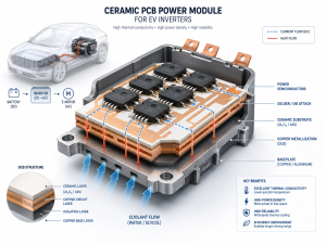
At EBest Circuit (Best Technology), design support is closely tied to manufacturing expertise. Design-for-manufacturability reviews ensure that multilayer PCB designs translate smoothly into reliable production, even for complex stack-ups.

What is the highest number of layers in a PCB?

There is no absolute limit to the number of layers in a PCB, but practical constraints define realistic boundaries. Commercial multilayer printed circuit boards commonly range from four to twenty layers. Advanced systems may use thirty or more layers when required.

In high-performance computing and aerospace applications, extremely high layer counts have been achieved. These designs demand precise control of materials, lamination cycles, and registration accuracy. Each added layer increases complexity and cost.

More layers provide routing flexibility and power integrity, but they also introduce manufacturing challenges. Balance is essential.

Experienced manufacturers guide customers toward optimal solutions rather than maximum complexity. The goal is not to use the most layers, but the right number of layers to meet performance and reliability goals.

Multilayer printed circuit board, Multilayer PCB application

What is the purpose of having multiple layers in a PCB?

The primary purpose of multiple layers in a PCB is functional separation. Different electrical roles are assigned to dedicated layers, improving performance and predictability. Signal layers carry data. Power layers distribute energy. Ground layers provide stable references.

This separation enhances signal integrity by reducing noise coupling and crosstalk. It also supports efficient power distribution, which is critical in modern electronics with fast switching devices.

Multilayer printed circuit boards also enable compact product design. By routing signals vertically through vias, designers reduce board area while maintaining functionality.

Thermal performance is another key benefit. Internal copper planes act as heat spreaders, helping manage temperature rise. When designed correctly, multilayer structures contribute directly to long-term reliability.

What are the advantages of multilayer PCBs?

Multilayer PCBs offer several compelling advantages that make them the preferred choice for advanced electronics.

  • One major benefit is improved electrical performance. Shorter signal paths and controlled impedance support high-speed operation.
  • Another advantage is mechanical stability. Laminated layers create a rigid structure that resists warping and vibration.
  • Design flexibility also increases with layer count. Engineers can route complex circuits without overcrowding, improving yield and manufacturability.
  • From a system perspective, multilayer printed circuit boards enable integration. More functionality fits into less space, reducing assembly complexity.

How do multilayer PCBs work?

Multilayer PCBs work by distributing electrical functions across stacked conductive layers. Signals travel through copper traces on designated layers, while power and ground planes provide stable electrical environments.

Vias connect these layers vertically, creating three-dimensional routing paths. This structure allows complex interconnections without excessive surface congestion.

The internal planes also act as capacitive elements. Power bus decoupling on multilayer printed circuit boards benefits from closely spaced power and ground layers.

Manufacturing precision ensures that each layer aligns correctly. Lamination bonds layers into a single unit, while drilling and plating create reliable interconnections. The result is a cohesive electrical platform designed to perform consistently.

What is the difference between single layer and multilayer PCB?

The difference between single layer and multilayer PCB lies in complexity, capability, and application scope. A single-layer board has one conductive layer and is suitable for simple circuits. It offers low cost and straightforward manufacturing.

A multilayer PCB, by contrast, supports complex routing and higher performance. Multiple layers enable better signal control, power distribution, and noise reduction.

Single-layer boards struggle with high-speed signals and dense layouts. Multilayer printed circuit boards handle these challenges with structured stack-ups and dedicated planes.

The choice depends on requirements. Simple products benefit from simplicity. Advanced systems demand multilayer solutions.

Multilayer printed circuit board, Multilayer PCB application

Common multilayer PCB application scenarios

Multilayer PCB application spans nearly every advanced electronic sector.

  • Consumer electronics rely on multilayer printed circuit boards to support compact, feature-rich devices. Smartphones and tablets are prime examples.
  • In medical electronics, multilayer designs support precision, reliability, and miniaturization. Diagnostic equipment and monitoring systems depend on stable signal integrity and controlled power distribution.
  • Automotive systems use multilayer PCBs for safety-critical functions. Engine control units, driver assistance systems, and infotainment platforms all benefit from multilayer architecture.
  • Industrial equipment also relies heavily on multilayer PCB application. Automation, robotics, and power control systems require robust designs that withstand harsh environments.
Across all these scenarios, manufacturing consistency matters. EBest Circuit (Best Technology) integrates multilayer PCB manufacturing with assembly and testing, delivering complete Turnkey EMS solutions that support diverse applications.

Conclusion:

Multilayer printed circuit boards form the foundation of modern electronics. They enable compact design, stable performance, and functional integration across industries. From material selection to stack-up design, every decision shapes reliability and efficiency.

Choosing the right partner is just as important as choosing the right layer count. If you are planning a multilayer PCB project or need full Turnkey EMS support, EBest Circuit (Best Technology) is ready to help.

For technical consultation or quotations, contact sales@bestpcbs.com

You may also like

What is a BMS PCB Board? BMS PCB Protection Board for 18650

December 12th, 2025

A BMS PCB board (Battery Management System Printed Circuit Board) is the essential protection and control system used in lithium battery packs, especially in 18650, Li-ion, LiPo, and LiFePO₄ applications. From simple consumer electronics to EV battery packs, the BMS PCB ensures safe charging, stable discharging, cell balancing, and real-time battery monitoring.

This guide covers everything you need to know about BMS PCBs—including how they work, types, key functions, how to choose the right board, how to test it, and why EBest Circuit (Best Technology) is a trusted BMS PCB manufacturer.

What is a BMS PCB Board? BMS PCB Protection Board for 18650

What Is a BMS PCB Board?

A BMS PCB board is an electronic circuit board designed to monitor, protect, and balance lithium battery cells. It ensures that the battery pack stays within safe operating limits, avoiding overcharging, over-discharging, overcurrent, overheating, and short circuits.

A typical BMS PCB contains:

  • Protection IC
  • MOSFET charge/discharge control
  • Current shunt resistors
  • Temperature sensors
  • Balancing circuitry
  • Communication chips (CAN, UART, RS485, Bluetooth, etc.)
  • Thick-copper power traces
  • Thermistors and connector interfaces

Because lithium batteries are highly sensitive to voltage and current fluctuations, a BMS PCB ensures that every cell operates safely and efficiently.

Types of BMS PCB Board

BMS PCBs come in several categories based on battery type, cell configuration, communication, and protection function.

Types of BMS PCB Board

1. Based on Cell Configuration

  • 1S BMS – single-cell lithium battery
  • 2S–6S BMS – common for 18650 packs
  • 7S–16S BMS – used in e-bikes, scooters
  • 20S–24S and above – used in ESS and EV packs

2. Based on Balancing Method

  • Passive balancing BMS (energy dissipated through resistors)
  • Active balancing BMS (more efficient; redistributes energy between cells)

3. Based on Protection Function

  • Basic protection boards (Over/Under-voltage, Overcurrent)
  • Smart BMS (with Bluetooth, CAN, UART control, SOC/SOH monitoring)

4. Based on Application

  • 18650 battery packs
  • Power tools
  • E-bike batteries
  • Solar storage batteries
  • Medical devices

What Does a BMS Board Do?

A BMS PCB board (Battery Management System PCB) is the central controller responsible for ensuring that lithium battery packs operate safely, efficiently, and reliably. Since lithium batteries are sensitive to voltage, current, temperature, and balancing differences, the BMS acts as an intelligent guardian that constantly supervises the entire pack. Its functions including:

1. Overcharge Protection

2. Over-Discharge Protection

3. Overcurrent & Short-Circuit Protection

4. Temperature Protection

5. Cell Balancing

6. Charging/Discharging Control

7. SOC/SOH Estimation (Smart BMS)

8. Communication & Data Reporting (for smart BMS)

These features make the BMS the “brain” of a lithium-ion battery pack.

How Does a BMS Board Work?

A BMS PCB operates by continuously monitoring voltage, current, and temperature. Here is the basic workflow:

How Does a BMS Board Work?

1. Voltage Sensing

Each cell’s voltage is monitored through sense lines to prevent overcharge/over-discharge.

2. Current Measurement

A shunt resistor or Hall sensor measures current passing through the pack.

3. MOSFET Switching

The BMS activates or deactivates charging/discharging MOSFETs to protect the battery.

4. Temperature Monitoring

Sensors detect overheating and disable charging/discharging if needed.

5. Balancing Circuit

If one cell becomes higher than others, balancing resistors bleed excess charge until all cells match.

6. Control Unit (in Smart BMS)

A microcontroller processes data and communicates via CAN, UART, RS485, etc.

The result is a stable, safe, efficiently managed battery system.

What Is the Difference Between PCM and BMS?

FeaturePCM (Protection Circuit Module)BMS (Battery Management System)
Basic Protection✔ Overcharge / Overdischarge / Overcurrent✔ Includes PCM features
Cell Balancing❌ Usually none✔ Supports balancing
Communication❌ None✔ CAN, UART, RS485, Bluetooth
Data Logging❌ No✔ SOC, SOH, temperature, cycles
ComplexitySimpleAdvanced
ApplicationsSmall electronics, 18650 packsEVs, ESS, scooters, UPS

PCM = basic protection

BMS = complete monitoring and management system

What Is a BMS PCB Used For?

A BMS PCB is used in all lithium-ion battery applications, such as:

  • 18650 battery packs (flashlights, e-bikes, power tools)
  • Electric vehicles (EV, HEV, PHEV)
  • Energy Storage Systems (ESS)
  • Solar battery systems
  • UPS / backup power
  • Drones, UAVs, robotics
  • Medical devices
  • Smart home appliances
  • Portable electronics
  • E-scooters and e-motorcycles

Any application requiring safe lithium battery operation needs a BMS PCB.

Can I Run a Lithium Battery Without a BMS?

No — it is unsafe to run a lithium-ion battery without a BMS.

Without protection, lithium batteries can experience:

  • Overcharging → thermal runaway, fire, explosion
  • Over-discharging → permanent battery damage
  • Overcurrent → pack overheating
  • Cell imbalance → capacity drop, premature aging

Using a lithium-ion battery without a BMS is highly dangerous and not recommended.

How to Choose a PCB BMS Protection Board?

Selecting the right PCB BMS protection board is crucial for safety, performance, and battery lifespan. Here’s a detailed guide to help you choose correctly:

1. Select Based on Battery Chemistry

Different lithium chemistries have distinct voltage requirements:

Battery TypeMax Charge VoltageNeeds BMS?
Li-ion / NMC4.20V✔ Yes
LiPo4.20V✔ Yes
LiFePO₄3.65V✔ Yes

Using the wrong BMS for your chemistry may cause incorrect cutoff points.

2. Determine the Number of Series Cells (S Count)

A BMS must match the battery pack’s series number:

PackBMS Needed
3S (11.1V)3S BMS
4S (14.8V)4S BMS
7S (24V)7S BMS
10S (36V)10S BMS
13S (48V)13S BMS
16S (60V)16S BMS

3. Choose Continuous Discharge Current Rating

BMS current rating must exceed your maximum load.

ApplicationSuggested Current
Power banks3–10A
Tools / drones20–45A
E-bikes20–35A
E-scooters40–60A
ESS / inverter80–200A+

High current BMS PCBs require wide copper traces and heavy copper layers (2–10 oz).

4. Pick Balancing Type

  • Passive balancing → economical, good for small/medium packs
  • Active balancing → high efficiency, ideal for EV and solar storage

Choose based on expected lifetime and precision needed.

5. Decide Whether You Need Smart Communication

Choose Smart BMS if you need:

  • Real-time monitoring
  • CAN communication with motor controller
  • Bluetooth APP
  • RS485 for energy storage
  • SOC/SOH estimates

If not required, a simpler PCM or basic BMS is enough.

6. PCB Structure Requirements

For reliable high-power protection boards, a proper PCB structure is essential:

  • High TG material (TG ≥150°C)
  • Thick copper (2–4 oz or higher)
  • Reinforced pads for MOSFETs
  • Wide trace routing for current paths
  • Good thermal dissipation design
  • ENIG finishing for stable bonding

EBest Circuit (Best Technology) specializes in heavy-copper PCBs designed specifically for BMS modules.

7. Safety Certifications

Depending on product category/status:

  • UL
  • CE
  • RoHS
  • IEC62133
  • UN38.3

Choosing a compliant BMS PCB manufacturer enable to reduce risks and improves product reliability.

How to Test the BMS PCB Board?

Testing a BMS PCB board is crucial to ensure it performs safely and reliably before being integrated into a lithium battery pack. A well-designed Battery Management System must accurately sense voltages, manage current, protect against faults, and communicate with other system components. Below are 5 essential BMS PCB testing methods, each commonly used in manufacturing and engineering validation.

How to Test the BMS PCB Board?

1. Visual Inspection (Surface & Solder Joint Check)

Purpose: Identify obvious defects before powering the board.

How it works:

Technicians use AOI (Automated Optical Inspection) or manual magnification tools to check:

  • Solder bridge, cold solder joints
  • Component orientation errors
  • Missing or misplaced components
  • PCB surface damage, cracks, or contamination

This step ensures the board is physically ready for electrical testing and prevents short circuits during power-up.

2. Continuity & Insulation Test (Shorts and Opens Test)

Purpose: Verify PCB traces, vias, and components are correctly connected.

How it works:

Using a multimeter or flying-probe tester, engineers check:

  • Shorts between power rails
  • Open circuits on balancing lines
  • Proper grounding and isolation between channels

This test eliminates wiring errors that could cause BMS malfunction or overheating.

3. Cell Voltage Detection Accuracy Test

Purpose: Ensure the BMS measures each cell’s voltage correctly.

How it works:

A variable DC power source simulates individual battery cells. The tester adjusts voltage (e.g., 2.5V → 4.2V for Li-ion cells) and compares:

  • Actual input voltage
  • BMS measurement output (through UART/CAN/I²C or display)

Acceptable deviation is usually ±5–10 mV for quality BMS boards.
Accurate detection is crucial for safe charging and balancing.

4. Protection Function Test (OVP, UVP, OCP, SCP)

Purpose: Confirm the BMS triggers proper protection responses.

How it works:

Engineers simulate fault conditions:

  • Over-voltage protection (OVP): Gradually raise simulated cell voltage until BMS disconnects charging.
  • Under-voltage protection (UVP): Lower cell voltage until BMS cuts off discharging.
  • Over-current protection (OCP): Apply load current beyond spec to check if the MOSFET shuts off.
  • Short-circuit protection (SCP): Momentarily create a low-resistance path to verify BMS reacts instantly.

5. Balancing Function Test (Active/Passive Balance Check)

Purpose: Verify that the BMS can equalize cell voltages.

How it works:

Setting slight voltage differences between simulated cells. The BMS should under one of below situations:

  • Activate resistance bleeding (passive balance)
  • Transfer energy between cells (active balance)

Engineers measure:

  • Balance current
  • Trigger threshold
  • Balance response time

Balancing tests ensure better battery lifespan and capacity utilization.

EBest Circuit (Best Technology)’s BMS PCB Manufacturing Service

EBest Circuit (Best Technology) is a professional BMS PCB board and PCB & PCBA manufacturer with over 18 years of experience, providing high-reliability battery protection boards for lithium battery companies worldwide.

Why Choose EBest Circuit (Best Technology) for BMS PCB?

✔ 2–10 oz heavy-copper BMS PCBs

✔ High-TG board materials specialized for high-current

✔ IPC Class 2 & Class 3 manufacturing

✔ SMT + through-hole assembly for BMS MOSFETs/ICs

✔ 100% functional testing

✔ Customized 1S–30S BMS PCB solutions for 18650, LiFePO4, NMC

Industries We Support

  • E-bike & scooter battery manufacturers
  • Energy storage system providers
  • Drone and UAV companies
  • Power tool manufacturers
  • Custom lithium battery pack makers

If you need BMS PCB prototype, small batch, or mass production, EBest Circuit (Best Technology) provides fast turn-around and engineering support.

FAQs

1. What type of BMS do I need for 18650 batteries?

Choose a BMS based on your pack configuration (1S–13S), your total continuous current (5A–60A for standard packs), and whether you need balancing or communication. A BMS PCB protection board for 18650 should match the battery chemistry and voltage thresholds.
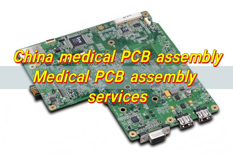
2. Does BMS drain the battery?

Yes, but only slightly. A typical BMS has very low standby current (10–100 µA), which minimally affects overall battery life. High-quality BMS PCBs have optimized low-power designs to reduce parasitic drain.

3. What is a BMS PCB board used for?

A BMS PCB board is used to protect, monitor, and manage lithium-ion battery packs. It prevents overcharge, over-discharge, overcurrent, overheating, and cell imbalance. BMS PCBs are commonly used in 18650 battery packs, e-bikes, EVs, solar systems, UPS units, drones, and portable electronics.

4. What is balancing in a BMS?

Balancing ensures all cells in a series pack maintain equal voltage. This prevents weak cells from becoming overstressed, improves efficiency, and extends battery lifespan. Balancing can be passive (bleeding excess charge) or active (redistributing charge).

5. Why is my BMS cutting off power?

Your BMS may cut off power due to:

  • Overcurrent
  • Short circuit
  • Over-discharge
  • Overcharge
  • High temperature
  • Cell voltage imbalance

6. How long does a BMS last?

A high-quality BMS PCB typically lasts 5–10 years, depending on usage, heat exposure, component quality, and environment. Industrial-grade BMS modules can last even longer.

7. What happens if a BMS fails?

If a BMS fails, the battery may overcharge, over-discharge, or overheat. This can lead to permanent cell damage or dangerous thermal runaway. Therefore, quality manufacturing and thorough testing are essential for preventing BMS failure.

You may also like

4 Layer Flex PCB Manufacturer, Over 19 Years

December 5th, 2025

What is a 4 layer flex PCB? This blog is mainly about thickness, stackup, design requirements and guideline, production process, cost for 4 layer flex PCB.

Are you worried about these issues?

  • How to avoid inter-layer interference and signal loss in 4-layer flexible PCBs with high routing density?
  • Flexible Durability Challenge: How to ensure over 100,000 bend cycles in repeated flexing scenarios?
  • How to balance quality and cost in multi-layer flexible PCB production?

As a 4 layer flex PCB manufacturer, EBest Circuit (Best Technology) can provide you service and solutions:

  • Free DFM Analysis: Leveraging 20 years of expertise, we provide free DFM analysis to identify risks early, optimize layer stacking and routing schemes, boost signal integrity by over 40%, reduce design iterations by 50%, and achieve 98% first-pass success.
  • Quality Enhancement: Using rolled annealed copper and adhesive-free FPC technology, our solution passes 200,000 dynamic bend tests (0.5mm radius, 30 cycles/min) with ≤5% resistance change and 30% reduced delamination risk, meeting 100,000 fold cycles for foldable smartphones.
  • Efficient Production Collaboration: Through supply chain integration and patented automated bending devices, we shorten production cycles to 15 days, cut costs by 20%, maintain ≥99.5% batch yield, and support 5G/millimeter-wave high-frequency applications.

Welcome to contact us if you have any request for 4 layer flex PCB: sales@bestpcbs.com.

What Is A 4 Layer Flex PCB?

A 4 layer flex PCB is a flexible printed circuit board with four conductive layers sandwiched between insulating films. Unlike rigid boards, it bends, twists, and fits into tight spaces. Think of it as a high-tech sandwich: layers of copper traces, dielectrics, and cover layers stacked to handle complex circuits without cracking. It’s perfect for gadgets that move, like foldable screens or medical implants.

4 Layer Flex PCB Manufacturer

How Thick Is a 4 Layer Flex PCB?

The typical thickness range for a four-layer flexible PCB (flexible circuit board) is between 0.2mm and 0.6mm. The specific value depends on the material combination (such as polyimide substrate thickness, copper foil weight), adhesive type (with or without adhesive), and the choice of surface coating/protective film. The core influencing factor is the cumulative thickness of the dielectric layers between each conductive layer (including copper foil) and the lamination process. Thinner designs can be achieved by using ultra-thin substrates (such as 12.5μm) and 1/3 ounce copper foil.

4 Layer Flex PCB Stackup

1. Top Copper Foil Layer

  • Thickness: 17-35μm electrolytic copper foil.
  • Function: Surface circuit layer, used for component soldering and signal transmission.

2. First Dielectric Layer

  • Material: Polyimide or epoxy resin; Thickness: 50-100μm.
  • Function: Insulating and isolating inner copper foil layers.

3. First Inner Layer

  • Thickness: 17-35μm electrolytic copper foil.
  • Function: Internal signal layer.

4. Second Dielectric Layer(Core Layer)

  • Material: Polyimide; Thickness: 100-200μm.
  • Function: Main supporting structure for inner copper foil layers.

5. Second Inner Layer

  • Thickness: 17-35μm electrolytic copper foil.
  • Function: Internal power/ground layer.

6. Third Dielectric Layer

  • Material: Polyimide or epoxy resin.
  • Thickness: 50-100μm.
  • Function: Insulation and isolation.
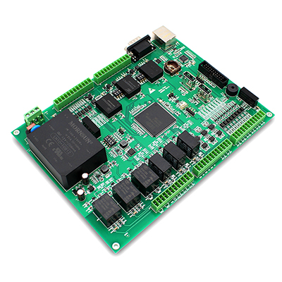
7. Bottom Copper Foil Layer

  • Thickness: 17-35μm electrolytic copper foil.
  • Function: Surface circuit layer.

4 Layer Flexible PCB Design Technical Requirements

Parameter NameRecommended Value/Requirement
Standard Stackup OrderTOP (Signal) – GND – PWR – BOTTOM (Signal)
FR4 Stiffener Width at Rigid-Flex Area≥5mm
Flexible Area Bend Radius≥10×Board Thickness (Dynamic Bending Scenario)
Substrate TypePolyimide (PI)
Copper Thickness (Signal Layers)0.5–1oz
Copper Thickness (Power/Ground Layers)1–2oz
Board Thickness Range0.1mm–0.3mm (Optional Thicker PI Reinforcement)
Minimum Trace Width/Spacing50μm/50μm (2mil/2mil)
Signal Trace Spacing (3W Rule)≥3×Trace Width
Power Layer Retraction (20H Rule)40–80mil (≈1.0–2.0mm)
Trace Direction in Flexible AreaPerpendicular to Bending Direction
Impedance Tolerance±7%
Distance Between Inner Signal Layer and Reference Layer≤0.1mm
Dynamic Bending Life≥1 Million Cycles (Curvature Radius 1mm)
Static Bending Angle≤90° (Avoid Sharp Bends)
Interlayer Dielectric Thickness≥0.1mm
Blind/Buried Via Tolerance (Backdrilling)±0.05mm
Warpage≤0.75%
Interlayer Insulation Resistance≥10¹²Ω (500VDC)
Temperature Test Range-55℃~125℃ (Military Standard)

4 Layer Flex PCB Design Guideline

A detailed design guideline for 4 layer flex PCB:

1. Stackup Strategy

  • Classic stackup: Top Signal – Ground Plane – Power Plane – Bottom Signal, prioritized for high-speed signal requirements. Alternative stackup (for high-current scenarios): Top Signal – Power Plane – Ground Plane – Bottom Signal, requiring trade-offs in high-speed performance.
  • Copper thickness symmetry control: Outer layers use 0.5–1oz rolled copper (superior bending resistance to electrolytic copper). Inner layers use 1oz electrolytic copper. TOP/power layer thickness difference ≤0.5oz to prevent warpage.

2. Rigid-Flex Area Design

  • FR4 stiffener width ≥5mm: Use ≤45° stepped pressing to distribute stress. Components/vias ≥1.5mm from bend line to avoid solder joint cracking.
  • Flex zone copper treatment: Large copper areas converted to mesh copper (opening ratio ≥70%). Trace direction perpendicular to bend axis. Dynamic bend radius ≥10× board thickness (e.g., 0.2mm board thickness requires ≥2mm radius).

3. Routing Rules

  • Geometric constraints: Minimum trace width/spacing 50μm/50μm (2mil/2mil). High-speed differential pairs prefer curved routing. No sharp 90° traces; flex zone corner radius ≥3× trace width.
  • Power integrity: Power plane retraction (20H rule) 1.0–2.0mm to suppress edge radiation. Decoupling capacitors placed ≤2mm from each IC power pin.
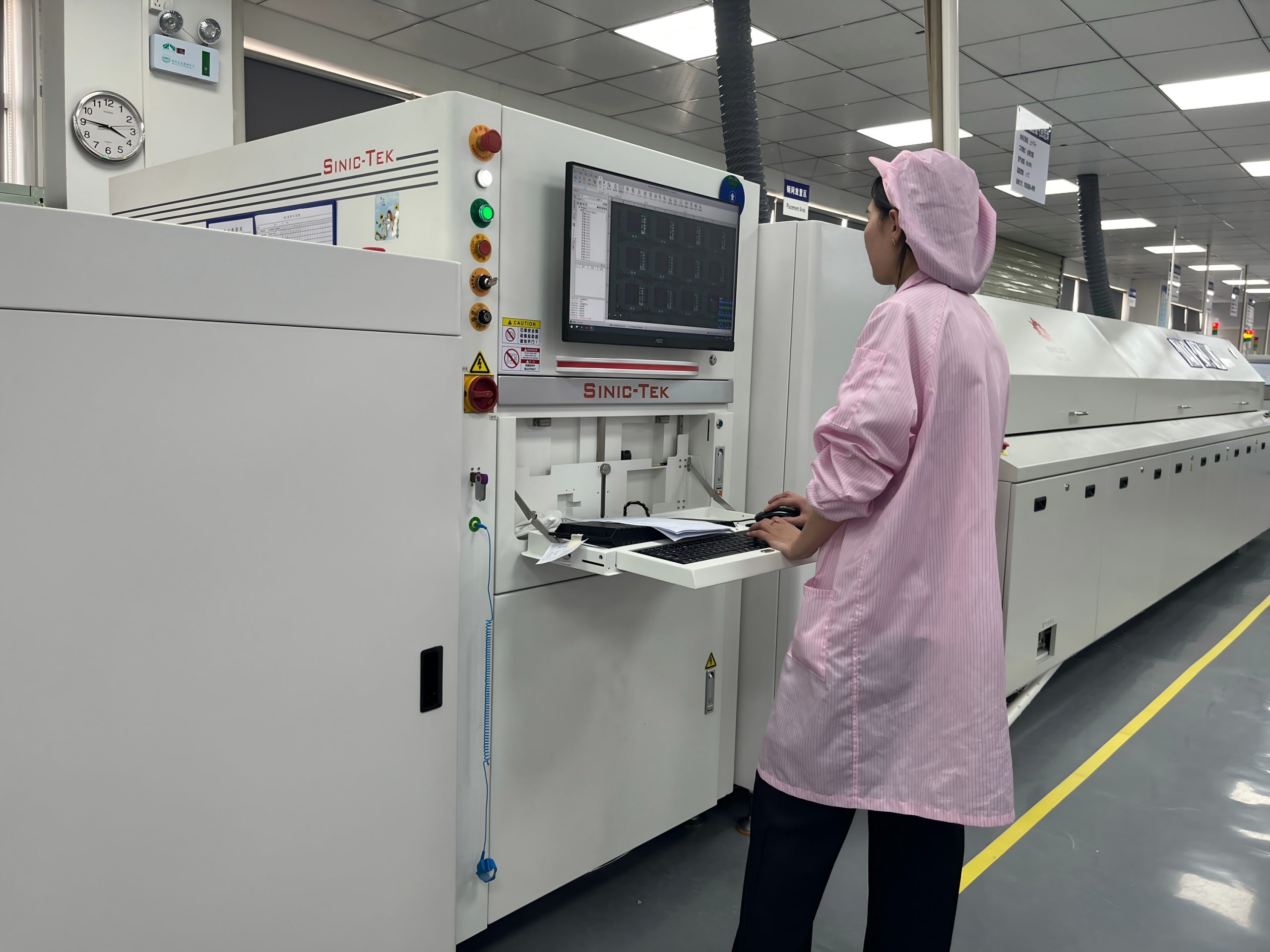
4. Via Reliability Design

  • Through-hole vias only for static areas, hole diameter ≥0.2mm, pad ≥0.4mm. Blind vias for high-speed signals (e.g., USB) connecting top-layer to L2, depth tolerance ±0.05mm.
  • Reinforce flex zone vias with teardrop pads. Buried vias only for clock signals between L2-L3 (cost increase 0.8%/via).

5. Material & Manufacturing Requirements

  • Substrate: Polyimide (PI) withstands >260°C, superior bending life to FR4. Coverlay thickness ≥0.1mm, covering pad edges ≥0.1mm.
  • Panel design: Flex boards spaced ≥2mm apart. Add 0.5mm stamping holes for depaneling. Process edge width ≥5mm for fixture clamping.

6. Pre-Fabrication Verification

  • Impedance control: High-speed lines (USB/HDMI) tolerance ±7%, reference layer spacing ≤0.1mm.
  • 3D bend simulation: Check component interference in Altium Designer (View > 3D Mode). Dynamic bend test ≥1 million cycles (curvature radius 1mm).
  • DFM confirmation: Components ≥3mm from rigid-flex edge to ensure manufacturability.
4 Layer Flex PCB Design Guideline

4-Layer Flex PCB Manufacturing Process

1. Material Preparation & Inner Layer Processing

  • Flexible zone substrate: Polyimide (PI) film, thickness 25–50μm, temperature resistance >260°C.
  • Rigid zone stiffener: FR-4, glass transition temperature (Tg) value ≥170°C.
  • Copper foil selection: Outer layer rolled annealed copper 0.5–1oz (anti-bending fatigue), inner layer electrolytic copper 1oz (cost-conductivity balance).
  • Pattern transfer: Dry film lamination at 110±5°C, pressure 0.4–0.6MPa. LDI laser exposure accuracy ≤10μm (eliminates alignment deviation).
  • Etching control: 1oz copper line width compensation +15μm. Minimum trace width/spacing 50μm/50μm (additional 10% width in flexible zone).

2. Multilayer Lamination Steps

  • Interlayer alignment: Rigid-flex zone uses PIN positioning system, interlayer offset ≤75μm. Coverlay window opening is 0.1mm larger than pad edge on one side (prevents tearing).
  • Lamination parameters: Heating rate 2–3°C/min, peak 185±5°C. Pressure 15–20kg/cm² (high pressure embrittles PI, low pressure causes delamination). High-temperature holding time 45–60min.
  • Flexible zone treatment: Pre-press at 0.5MPa low pressure for degassing, then high-pressure lamination (avoids bubble residue).

3. Drilling & Metallization Process

  • Hole types: Mechanical drilling diameter ≥0.2mm (rigid/through-holes). Laser drilling blind hole diameter 0.1mm (top-layer to L2 high-speed signal).
  • Hole position accuracy: Rigid-flex zone tolerance ±50μm (requires X-ray target correction).
  • Hole metallization: Electroless copper thickness ≥0.3μm. Pulse plating copper thickness uniformity error ≤15% (reduces hole necking).
  • Flexible zone reinforcement: Via pads with teardrop shape, pad diameter ≥ hole diameter ×2.2.

4. Outer Layer & Surface Finish

  • Coverlay instead of solder mask: PI coverlay thickness 0.1mm, adhesive flow control ≤0.3mm. Flexible zone window opening distance from trace edge ≥0.15mm (prevents stress concentration).
  • Surface finish: ENIG preferred for flex boards (nickel 3–5μm, gold 0.05–0.1μm for optimal solder joint ductility). Avoid HASL (prevents PI delamination).

5. Quality Validation & Reliability Testing

  • AOI inspection: Flexible zone trace width tolerance ±10%, rigid zone ±15% (zone-specific parameters).
  • 3D X-ray inspection: Blind hole fill ratio ≥85% (eliminates void soldering).
  • Dynamic bending test: Curvature radius 1mm, frequency 1Hz, cycles ≥500k (industrial standard).
  • Thermal shock test: -40°C↔125°C cycling, 1000 cycles later conduction resistance change ≤10%.
4 Layer Flex PCB Manufacturing Process

Why Choose EBest Circuit (Best Technology) as 4 Layer Flex PCB Manufacturer?

Reasons why choose EBest Circuit (Best Technology) as 4 layer flex PCB manufacturer:

  • 19 Years of Flex PCB Expertise: Decades of specialized experience in 4-layer flex PCBs translate to optimized stack-ups, impedance control, and material selection—saving engineers trial-and-error time.
  • Medical/Aerospace-Grade Certifications: Compliance with ISO 9001, IATF 16949, medical ISO 13485, and RoHS ensures seamless approval for regulated industries. Certifications reduce compliance headaches for international clients.
  • Cost-Sensitive Design Optimization: We engineer competitive pricing through DFM (Design for Manufacturing) analysis, eliminating costly design flaws before prototyping. Free DFM reports reduce iteration costs by up to 30% for cost-conscious projects.
  • Transparent Pricing Model: No hidden fees. Clear per-panel/material pricing with volume discounts helps engineers budget accurately for both prototypes and production runs.
  • 24-Hour Rapid Prototyping for Urgent Needs: Emergency orders receive 24-hour turnaround on 4-layer flex PCB samples, critical for hardware startups and medical device developers racing against launch deadlines.
  • 99.2% On-Time Delivery Reliability: Our supply chain excellence guarantees 99.2% of orders ship on schedule, minimizing project delays for engineers working under tight timelines.
  • 100% Batch Inspection: Every 4-layer flex PCB undergoes rigorous AOI, X-ray, and electrical testing. Full batch inspection eliminates hidden defects—a must for high-reliability applications like automotive and aerospace.
  • Turnkey One-Stop Solution: From design consultation and material sourcing to assembly and testing, we handle every step. Engineers save time by consolidating vendors into a single trusted partner.
  • Global Logistics & Customs Support: Our export-focused team navigates international shipping, tariffs, and documentation—critical for North American/European engineers sourcing from Asia.

How Much Does A 4-Layer Flex PCB Cost?

  • Consumer electronics field: Bulk purchase unit price is approximately $13-$20 per square meter, while prototyping costs increase to $138-$207 per square meter;
  • Automotive electronics/industrial control field: Due to high reliability requirements, the unit price generally rises to $25-$40 per square meter;
  • High-end medical/communication equipment field: Customized products using processes such as immersion gold and blind/buried vias can reach unit prices of over $50 per square meter.

Welcome to contact us if you have any other issue for 4-layer flex PCB: sales@bestpcbs.com.

You may also like

Top PCB Manufacturing Companies in UAE

December 4th, 2025

Looking for PCB manufacturing companies in UAE? This blog is mainly about list, selection guide, PCB types of PCB manufacturing companies in UAE.

PCB Manufacturing Companies in UAE are gaining attention due to local demand for electronics, automation, energy control modules, power conversion units, and security systems. PCB Manufacturing Companies in UAE also attract engineers who prefer short supply routes and fast communication. This article explains how the UAE market works, which suppliers are active, and how buyers can compare strengths before placing orders.
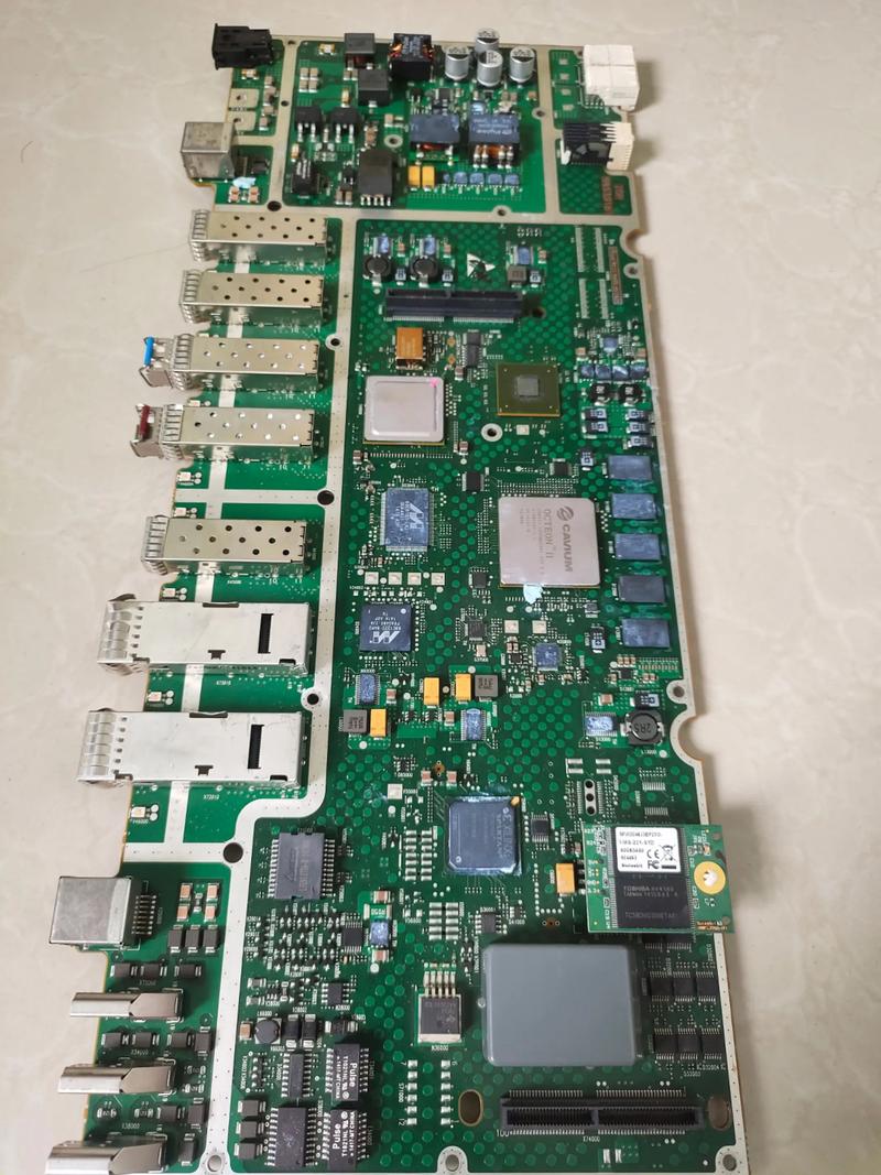
Top PCB Manufacturing Companies in UAE

List of PCB Manufacturing Companies in UAE

1. PCB Power Market

  • Main Business: Quick-turn PCB fabrication, prototype builds, and small-batch manufacturing.
  • Advantages: Stable quality for low-layer FR4 boards, simple quote process, and friendly service for students and hobbyists.
  • Production Capability: 1–8 layers, standard TG materials, HASL/ENIG finishes, basic impedance builds.
  • Lead Time: 5–12 working days for standard orders, with express service available.

2. EMatrix Electronics

  • Main Business: PCB manufacturing, PCB assembly, component sourcing, box-build, and embedded system support.
  • Advantages: Local engineering communication, on-site support, and guidance for PCB redesign when needed.
  • Production Capability: 2–10 layers, FR4, high-TG, ENIG, HASL, stencil production, and small SMT runs.
  • Lead Time: 7–14 working days depending on the part count and assembly density.

3. Al Taj

    • Main Business: Custom PCB fabrication, cable assembly, wiring harness production, and industrial electronics assembly.
    • Advantages: Good for mixed projects that require both board manufacturing and custom wiring.
    • Production Capability: 2–6 layers, FR4 boards, basic SMT assembly, through-hole assembly, and cable-board integration.
    • Lead Time: 10–18 days depending on project size.

    4. GREAT Waters

      • Main Business: PCB prototyping, PCB assembly, reverse-engineering, firmware programming, and repair services.
      • Advantages: Suitable for maintenance teams and companies upgrading older devices.
      • Production Capability: 1–6 layers, rework, redesign, simple RF routing, and mixed-technology assembly.
      • Lead Time: 8–15 days for PCB builds and assembly.

      5. Atlantis Engineering

        • Main Business: Custom electronics development, PCB fabrication, firmware, IoT product support, and prototype assembly.
        • Advantages: Good for early-stage product design, enclosure design, and complete device planning.
        • Production Capability: 2–6 layers, low-run PCB assembly, IoT module integration, and EMC-aware redesign.

        • Lead Time: 12–20 working days.

        6. Fastron Group Partners

          • Main Business: PCB manufacturing from international production lines, plus stocking of RF inductors and passive components.
          • Advantages: Good component availability for RF boards, radio modules, and mixed-signal circuits.
          • Production Capability: 2–12 layers, controlled impedance, ENIG finishes, and RF materials on request.
          • Lead Time: 12–20 days based on factory load.

          7. Al Mashriq Electronics

            • Main Business: PCB design, PCB manufacturing coordination, on-site testing, and EMC trouble-shooting.
            • Advantages: Strong design support and hands-on debugging for local users.
            • Production Capability: 2–6 layers, stencil support, DIP assembly, and bench-level testing.
            • Lead Time: 10–16 working days.

            How to Select PCB Manufacturing Companies in UAE?

            A detailed selection guide to PCB manufacturing companies in UAE:

            1. Prioritize Certification Compliance

              • ECAS Mandatory Certification: All PCBs exported to the UAE must pass ECAS certification from the Emirates Authority for Standardization and Metrology (ESMA), covering safety, electromagnetic compatibility, energy efficiency, and other standards. Technical documents, circuit diagrams, PCB layout drawings, and test reports from local certified laboratories (such as IEC 60335 and CISPR standards) must be provided in Arabic.
              • MPCI Declaration System: As of July 2025, all shipments must submit container data to the UAE National Advance Information Center (NAIC) in advance, including bill of lading numbers, HS codes, and cargo values. The grace period extends until March 2026, with fines for non-compliance.
              • Localization Requirements: Non-UAE companies must appoint a local agent or authorized representative and ensure product labels include Arabic information (such as model numbers, electrical parameters, and manufacturer addresses).

              2. Match Technical Capabilities

                • Advanced Technical Support: Prioritize manufacturers with capabilities in HDI (High-Density Interconnect), FPC (Flexible Printed Circuit), rigid-flex boards, and package substrates (such as ABF carriers) to meet high-precision requirements for 5G, AI servers, and new energy vehicles.
                • Process Control Standards: Focus on hard indicators such as solder joint penetration rate (≥75%), insulation resistance (>1000MΩ), and dimensional tolerance (±0.5mm), as well as reliability verification through thermal cycling tests (-40°C to 125°C, 1000 cycles) and salt spray tests.
                • Environmental Material Application: Use halogen-free substrates (compliant with IEC 61249-2-21), bio-based resins, and biodegradable materials, certified under RoHS and REACH, to reduce hazardous substances like lead and cadmium.

                3. Manage Cost and Lead Time

                  • Price Transparency: Bulk orders are typically priced per solder joint (3-5 RMB/PINS), with sample prototyping fees starting at approximately 50 RMB. Complex designs require additional quotes. Compare bulk discounts and rush fee policies (such as JLCPCB’s 12-hour/24-hour expedited services).
                  • Lead Time Guarantee: Confirm production cycles (e.g., 12-72 hours for samples, with clear cut-off times and production scheduling rules for bulk orders) and consider logistics time (sea freight approximately 30 days, air freight 3-5 days) to avoid delays impacting project timelines.
                  • Supply Chain Resilience: Evaluate manufacturers’ raw material procurement channels (e.g., copper foil, resin), inventory management capabilities, and capacity adjustment flexibility to respond to sudden demand changes.

                  4. Quality Control Systems

                    • Incoming Material Inspection: Conduct pre-warehouse inspections of PCB substrates (FR-4, high-frequency materials) and components for appearance and electrical performance to prevent defective items from entering the production line.
                    • Process Monitoring: Implement XRF screening for hazardous substances, ICP-MS for precise limit detection, solder joint AOI (Automated Optical Inspection), and ICT (In-Circuit Test) to ensure soldering quality and electrical performance.
                    • Final Product Verification: Perform insulation resistance tests, voltage withstand tests, functional tests (simulating actual operating conditions), and environmental adaptability tests (high-low temperature aging, vibration, and impact tests).

                    5. Localized Service Support

                      • Language and Communication: Ensure technical teams provide bilingual (English/Arabic) communication to promptly respond to design changes and technical inquiries.
                      • After-Sales Guarantee: Establish a quality issue feedback mechanism, offering quick repair, replacement, and return services, and support on-site factory audits for clients (some high-risk products require factory inspections).
                      • Market Insights Monitor: UAE industrial policies (such as Dubai Free Zone tax incentives), industry trends (such as growing demand for 5G base stations and electric vehicle BMS), and select partners with local market experience.
                      How to Select PCB Manufacturing Companies in UAE

                      PCB Types Offered by PCB Manufacturing Companies in UAE

                      PCB Types Offered By UAE PCB Manufacturing Companies:

                      • Single-layer PCBs: Used for lighting products, basic power supplies, and simple sensors.
                      • Double-layer PCBs: Suitable for control panels, audio devices, and security modules.
                      • Multilayer PCBs (4–10 layers): Common in telecom systems, industrial automation, and embedded modules.
                      • Aluminum PCBs: Often used for LED lighting and power circuits requiring heat control.
                      • High-TG PCBs: Applied in automotive electronics and energy equipment.
                      • Rigid-flex PCBs: Sometimes available through UAE design houses but fabricated offshore.
                      • RF PCBs: Usually sourced from global suppliers, as local plants have limited capability.
                      PCB Types Offered by PCB Manufacturing Companies in UAE

                      Delivery Delays: China-UAE DDP Direct Shipping

                      Many UAE buyers experience long delivery times when working with suppliers who depend on slow freight channels or inconsistent shipping agents. These delays disrupt testing schedules and affect assembly timelines. Some factories also provide unclear transit updates, leaving customers unsure about the actual arrival date of their order. The result is more waiting, higher internal pressure, and frequent production rescheduling.

                      However, EBest Circuit (Best Technology) solves this with stable China–UAE DDP direct shipping. Our dedicated logistics channels shorten transit time and provide predictable delivery for both prototypes and mass production. We also handle customs clearance, duty processing, and local import steps, so customers avoid paperwork and hidden administrative tasks. Even better, our team tracks every shipment and updates clients throughout the journey. This ensures that UAE engineers can plan assembly work with confidence and move projects forward without disruptions.

                      PCB Quality Defects: Free DFM Audits Before Production

                      Some PCB manufacturers accept customer files without proper review. This leads to hidden design issues such as incorrect drill spacing, thin copper near vias, or solder mask misalignment. These problems often appear only after fabrication, resulting in failed tests, extra costs, and repeated revisions. UAE customers report that this situation causes major delays in new product development.

                      EBest Circuit (Best Technology) avoids these issues by providing free DFM audits before production. Our engineering team reviews Gerber files, stack-ups, drill charts, impedance needs before any board enters the line. This early check catches potential defects and gives customers practical suggestions to improve reliability. We also apply strict AOI, electrical testing, and controlled impedance checks to ensure that every board meets the expected standard. With this approach, UAE customers enjoy stable quality, fewer surprises, and smoother product launches.

                      Slow After-Sales Support: Technical Team 48H Online Response

                      When buying from some PCB manufacturers, clients often wait several days for technical support. This slow feedback becomes a serious obstacle during debugging, layout revisions, or NPI trials. Some suppliers only provide basic answers, which does not help engineers solve complex PCB or assembly issues. These delays extend development cycles and hurt time-to-market plans.

                      EBest Circuit (Best Technology) improves this experience with a technical team that responds within 48 hours. Our engineers cover CAM analysis, fabrication processes, SMT optimization, impedance guidance, and stack-up planning. UAE buyers receive clear explanations instead of generic comments. We also support PCBA troubleshooting with layout reviews, component alignment checks, and process suggestions. This fast and professional assistance helps customers maintain their project timeline and resolve issues quickly. It also builds stronger technical confidence throughout the production cycle.

                      Hidden Costs: All-Inclusive Pricing Without Extra Cost

                      Many PCB manufacturers offer attractive initial quotes but later add charges for tooling, testing, documentation, packaging, and even export handling. These hidden fees complicate budgeting and often result in higher-than-expected total cost. UAE procurement teams mention that this lack of transparency creates frustration and slows approval processes.

                      To avoid this, EBest Circuit (Best Technology) provides all-inclusive pricing with no unexpected fees. Our quotations cover material, drilling, plating, surface finishing, AOI, electrical test, and export documentation. For PCBA orders, we include SMT, DIP, testing, and component sourcing in a clear breakdown. Customers know the total cost from the start, which helps finance teams plan without uncertainty. This transparent pricing makes project management easier and helps buyers work more efficiently.

                      Case Studies of Our UAE PCB Manufacturing Project

                      Project Background

                      A UAE-based industrial equipment manufacturer required custom high-performance PCB components for new product development. Operating in a high-temperature Middle Eastern environment, the client demanded exceptional PCB durability and long-term stability, alongside rapid response capabilities for market launch needs.

                      Project Requirements

                      • Compliance with IPC-6012 Class 2 standards, ensuring stable electrical performance at 125°C continuous operating temperature. Vibration resistance must pass IEC 68-2-6 testing.
                      • Signal path impedance matching required 50±5Ω control, validated via Time-Domain Reflectometry (TDR).
                      • Sample delivery within 14 working days, accompanied by comprehensive DFM (Design for Manufacturing) analysis reports and reliability test data packages.

                      Solution

                      • Utilized FR-4 substrate with CTI ≥175 and thermosetting resin system to enhance high-temperature resistance. Vacuum lamination minimized interlayer voids, improving mechanical strength.
                      • Implemented parallel engineering across design, production, and testing phases: EDA software for signal integrity simulation, X-ray drilling alignment for precision, and dual AOI/flying probe systems for defect detection.
                      • Deployed digital production management for real-time process parameter monitoring and automatic deviation alerts to maintain stable process windows.

                      Result

                      • Samples passed client acceptance tests with 100% first-pass yield. Impedance deviations stayed within ±4.2Ω, and post-thermal aging electrical degradation remained below 2%, exceeding expectations.
                      • Bulk order delivery time reduced to 13 days, achieving 97.8% production yield with zero critical defects. Client recognized the project as “exceeding industry benchmarks.”
                      • Full digital quality traceability provided, including material batch records, process parameters, and test reports, enabling real-time remote verification by the client.

                      Why Choose EBest Circuit (Best Technology) for Global PCB Manufacturer?

                      Reasons why choose us for global PCB manufacturer:

                      • 19-Year Expertise: Leverages 19 years of industry experience with standardized process libraries and failure case databases to quickly identify design risks and provide proven solutions, reducing engineer trial costs.
                      • Certified Compliance: Holds ISO 9001, IATF 16949 automotive, ISO 13485 medical, and RoHS certifications to satisfy EU, Middle East, and other market access requirements while mitigating compliance risks.
                      • Competitive Pricing: Delivers cost-sensitive design solutions through material optimization and process innovation, reducing BOM costs by 15%-20% while meeting IPC-6012 standards, ideal for budget-sensitive consumer electronics projects.
                      • Rapid Prototyping: Enables 24-hour turnaround for urgent orders with TDR impedance validation and AOI inspection, accelerating prototype verification for designers and cutting product launch cycles by over 30%.
                      • 99.2% On-Time Delivery: Ensures 12-14 day standard lead times and 7-day express delivery for urgent orders via intelligent production scheduling and global supply chain coordination, meeting procurement stability demands.
                      • Batch Inspection Quality Control: Implements 100% inspection coverage during mass production with flying probe testing and reliability verification, maintaining over 98% yield rates for zero-defect assurance to engineers.
                      • Free DFM Analysis: Offers complimentary design-for-manufacturing reports during design phase, including signal integrity simulation, impedance matching recommendations, and solderability optimization to preempt production issues.
                      • Transparent Traceability: Maintains digital records of material batches, process parameters, and test data with unique ID tracking, enabling real-time quality verification for international procurement transparency needs.

                      Welcome to contact us to get a free quote if you have any request for PCB design, prototyping, mass production and assembly: sales@bestpcbs.com.

                      You may also like

                      Best UK PCB Manufacturer, PCB Manufacturing UK​

                      December 4th, 2025

                      Are you looking for best UK PCB manufacturer? This blog is mainly about how to choose, evaluate production capability and delivery time for best UK PCB manufacturer.

                      As a Chinese PCB manufacturer focusing on the global market over 19 years, EBest Circuit (Best Technology) are dedicated to providing cost-effective PCB solutions for our UK customers. Our core strengths enable you to find the optimal balance between cost, timeliness, and quality, making us your reliable global PCB manufacturing partner.

                      Best UK PCB Manufacturer

                      Are You Struggling With the Following Questions?

                      • Prolonged PCB prototyping lead times, with unfulfilled promises of 8-hour expedited prototyping, seriously delaying R&D progress.
                      • Lack of professional review for design schemes, leading to unfeasible processes only discovered during mass production and soaring rework costs.
                      • Opaque manufacturing processes, with no way to trace responsibilities when issues like cold solder joints and circuit offsets occur.
                      • Rejection of special process requirements, making it difficult to find contractors for customized orders such as multi-layer PCBs and flexible PCBs.
                      • Frequent changes in delivery times and unsubstantiated verbal commitments, forcing downstream production lines to shut down.

                      Our Solutions to These Questions

                      • Free DFM Pre-Review to Avoid Design Rework: Our engineer team completes design review within 24 hours, uses Cadence software to simulate mass production feasibility, marks issues such as circuit conflicts and impedance deviations, and provides optimization solutions, helping designers save over 30% of modification time.​
                      • Full-Process Quality Control to Ensure Engineering Reliability: There are 16 inspection procedures from copper-clad laminate incoming inspection to finished product delivery. With triple checks including AOI optical inspection, X-ray flaw detection and ICT online testing, the defect rate is controlled within 0.2%, meeting engineers’ requirements for product stability.​
                      • Express Delivery to Connect Production Plans: The fastest delivery time for 1-piece prototype is 8 hours, and bulk orders can be delivered to the UK within 4-7 days. Emergency orders activate the air freight green channel, which is 40% shorter than the industry average lead time, avoiding the risk of production suspension for purchasers due to delays.​
                      • Customized Processes to Meet Special Needs: Supporting 0.1mm fine line width and 0.2mm small aperture processing, the dielectric constant deviation of high-frequency boards is ≤±3%, and the flexible boards can withstand 100,000 bending cycles, meeting the technical requirements of engineers in high-end fields such as communications and medical care.​
                      • Transparent Collaboration to Reduce Purchasing Communication Costs: A production schedule is provided upon order signing, key processes are fed back with real-time photos, and quality inspection reports are delivered together with goods. Purchasers do not need to follow up repeatedly and can easily control the entire process.

                      Why Choose EBest Circuit (Best Technology) for Global PCB Manufacturer?

                      • Comprehensive and Compliant Authoritative Certifications: Holding ISO13485 (medical), IATF16949 (automotive), REACH and RoHS certifications, products comply with EU CE standards, so purchasers do not need to worry about access issues.
                      • Transparent Pricing with No Hidden Costs: Detailed quotations are provided, listing raw material costs, processing fees, inspection fees and logistics fees one by one. There are no additional charges in the later stage, allowing purchasers to accurately calculate costs with more secure budgets.
                      • Strict Quality Control and Outstanding Quality: An ISO9001 quality system is established, equipped with 20 sets of imported inspection equipment. Each batch of products is accompanied by third-party inspection reports. Automotive-grade PCBs pass high and low temperature cycle tests (-40℃ to 125℃) with stable performance.
                      • Fast and Stable Delivery: Owning 3 major production bases with a monthly capacity of 500,000 square meters, and the stock of commonly used base materials exceeds 100 tons. A transit warehouse is set up in the UK, with a 99.8% on-time delivery rate for regular orders, and emergency orders can be prioritized.
                      • Free DFM Design Support: Exclusive engineers provide one-on-one communication, not only identifying design issues but also optimizing processes to reduce production costs, helping designers achieve seamless connection between design and mass production.
                      • Cost Advantages of Global Supply Chain: Relying on China’s PCB industrial cluster, the procurement cost of raw materials is 15% to 20% lower than that in Europe, with no middlemen markup, providing purchasers with cost-effective options.
                      • Flexible Adaptation to Various Orders: Supporting R&D prototyping from 1 piece to mass production of 100,000 pieces, with no minimum order threshold for small-batch orders. The process switching cost is 25% lower than that of peers, meeting the differentiated needs of start-ups and large enterprises.
                      • Native English-Speaking Exclusive Service: 7×24-hour English customer service response, daily updates on order progress, and solutions for quality issues provided within 24 hours, ensuring barrier-free communication for purchasers.
                      Why Choose EBest Circuit (Best Technology) for Global PCB Manufacturer

                      Best UK PCB Manufacturer List

                      1. Our PCB Ltd

                      • Core Business: PCB prototyping and small-batch production, covering industrial and consumer electronics fields
                      • Advantages: Rapid response for 8-hour expedited prototyping service, real-time production progress updates, and customers can check at any time through the exclusive system, especially suitable for emergency R&D projects
                      • Process Capability: Manufacturing of 1-24 layer high multi-layer PCBs, flexible PCBs and metal substrates, supporting impedance control and resin plugging processes, with a minimum line width of 0.15mm
                      • Lead Time: 8-hour delivery for expedited prototyping, 3-5 days for regular orders, and 7-10 days for bulk orders

                      2. EC Electronics

                      • Core Business: Integrated PCB manufacturing and SMT assembly services, focusing on automotive electronics and industrial control fields
                      • Advantages: 40 years of industry experience, 99.5% delivery rate for bulk orders, long-term cooperation with multiple UK automotive companies, and sound quality traceability system
                      • Process Capability: Manufacturing of blind and buried via PCBs and high-power density circuit boards, supporting the entire SMT assembly process and enabling integrated delivery of PCBs and components
                      • Lead Time: 10-15 days for standard orders, 20-25 days for bulk customized orders, supporting partial delivery

                      3. Cambridge Circuit Company Ltd

                      • Core Business: PCB prototype and small-batch production, serving scientific research institutions and start-ups
                      • Advantages: ISO9001 quality system certification, transparent quotation with no hidden costs, outstanding cost-effectiveness for small and medium-batch orders, and timely response from the technical support team
                      • Process Capability: Manufacturing of single and double-layer PCBs, multi-layer PCBs (up to 12 layers) and flexible PCBs, with an exclusive production line for prototypes and mature and stable processes
                      • Lead Time: 5 days for standard orders, 3 days for expedited orders, and R&D samples can be prioritized

                      4. GSPK Circuits

                      • Core Business: Specialized PCB manufacturing, focusing on medical equipment and aerospace fields
                      • Advantages: Lean Champion certified enterprise, fast response for customized solutions, rich cases of medical equipment PCBs, and compliance with strict EU medical industry standards
                      • Process Capability: Manufacturing of 1-24 layer PCBs, lead-free surface treatment, supporting the production of circuit boards with special materials such as ceramics and polyimide, with excellent temperature resistance and stability
                      • Lead Time: 7-12 days for standard orders, 15-20 days for special material orders, with expedited service available (additional fees apply)

                      5. Rush PCB UK Ltd

                      • Core Business: High-end communication PCB manufacturing, serving communication equipment manufacturers and university R&D projects
                      • Advantages: Focus on high-end communication fields, impedance control accuracy of ±5%, and R&D cooperation with multiple UK universities
                      • Process Capability: Manufacturing of high-frequency and high-speed PCBs, rigid-flex boards, supporting a minimum line width of 0.1mm and a minimum aperture of 0.2mm, with outstanding signal integrity optimization capabilities
                      • Lead Time: 8-10 days for regular orders, 12-15 days for high-frequency and high-speed PCB orders, and 5-7 days for R&D samples

                      How to Choose a Reliable UK PCB Manufacturer?

                      A detailed selection guide to UK PCB manufacturer:

                      1. Verify the Authenticity of Qualification Documents

                      • Prioritize manufacturers holding authoritative certifications such as ISO9001 (basic quality), IATF16949 (automotive), and ISO13485 (medical). Request original certification documents for verification to avoid the risk of forged qualifications and ensure compliance with quality systems.

                      2. Conduct In-Depth Inspection of Production Entities

                      • Confirm whether they have their own factories and core production equipment (such as fully automated drilling machines and AOI inspection equipment) through online videos or on-site visits. Clarify whether the production links are outsourced to avoid choosing trading enterprises that only act as intermediaries and ensure production controllability.

                      3. Comprehensively Evaluate Technical Capabilities

                      • Gain a detailed understanding of their production experience in special processes such as multi-layer PCBs, flexible PCBs, and high-frequency and high-speed PCBs. Request 3-5 successful cases in similar industries and corresponding test reports to determine whether the technology matches the needs of your own projects.

                      4. Strictly Verify Delivery Capabilities

                      • Inquire about the on-time delivery rate data of the past 12 months, request an explanation of exclusive response plans for emergency orders (such as standby production lines and priority scheduling mechanisms), and clarify compensation clauses for delays to avoid affecting the progress of your own projects.

                      5. Focus on Value-Added Service Details

                      • Confirm whether free value-added services such as DFM design review and PCB performance optimization suggestions are provided. Understand the after-sales response process, including whether there is 7×24-hour customer service and how soon solutions can be provided after quality issues are reported, to ensure a full-process service experience.

                      6. Rationally Analyze Cost Structure

                      • Request detailed quotation breakdowns (raw materials, processing fees, inspection fees, etc.), compare the cost structures of different manufacturers, remain vigilant against the trap of “low-price attraction plus later price increases”, and focus on the cost-effectiveness of quality and price rather than simply pursuing low prices.

                      7. Conduct Multi-Channel Research on Customer Reputation

                      • Understand the market reputation of manufacturers through channels such as the UK Electronics Industry Association and professional forums. Prioritize manufacturers with service experience in similar industries. If necessary, contact their existing customers to obtain real cooperation feedback and reduce cooperation risks.

                      8. Confirm Supply Chain Stability

                      • Inquire about the supplier list and inventory cycle of core raw materials (such as copper-clad laminates and copper foil). Understand the response measures in the face of raw material price fluctuations or supply chain disruptions to ensure that orders will not be suspended due to material issues.

                      9. Clarify Intellectual Property Protection

                      • Include intellectual property protection clauses in the formal cooperation contract. Require manufacturers to promise not to disclose design drawings and technical parameters, and not to use customers’ PCB designs for other commercial purposes to ensure the security of core technologies
                      How to Choose a Reliable UK PCB Manufacturer

                      How to Evaluate the Production Capability of a UK PCB Manufacturer?

                      Methods about how to evaluate the production capability of a UK PCB manufacturer:

                      1. Check the production equipment list to confirm whether core equipment such as fully automated drilling machines, AOI inspection equipment, and X-ray inspection machines are available.

                      2. Understand the production capacity scale, inquire about the average monthly production area and maximum order undertaking capacity to determine whether it can match the needs of your own mass production.

                      3. Inspect the scope of process coverage, confirm the parameters of PCB layers, board thickness, line width and line spacing that can be produced, and whether they meet the project specifications.

                      4. Review the quality control system, request SOP (Standard Operating Procedures) and historical quality inspection reports to understand the defect rate data.

                      5. Evaluate flexible production capabilities, inquire about the production cycle and switching efficiency of small-batch orders to determine whether they can meet the needs of multiple varieties.

                      6. Understand the raw material supply system, confirm whether there is a stable list of qualified suppliers and whether there is an emergency material reserve mechanism.

                      7. Inspect the team configuration, understand the working years and professional qualifications of engineers and technical workers to determine the technical support capabilities.

                      8. Visit the production site (online or offline) to observe the production order, equipment maintenance status and workshop environment management level.

                      How to Evaluate the Production Capability of a UK PCB Manufacturer

                      How to Evaluate the Delivery Time of a UK PCB Manufacturer?

                      Methods about how to evaluate the delivery time of a UK PCB manufacturer:

                      1. Request a breakdown of delivery time components, clarify the specific time for document review, material procurement, production and processing, inspection and packaging, and other links.

                      2. Inquire about material inventory status, confirm the inventory cycle of commonly used components to determine whether the procurement link time can be shortened.

                      3. Understand the production line priority mechanism, confirm whether there is exclusive production line support for emergency orders and the implementation capacity of expedited services.

                      4. Verify historical delivery data, request delivery records of the past 6 months to calculate the on-time delivery rate.

                      5. Confirm the logistics cooperation model, whether there is long-term cooperation with well-known local logistics enterprises and whether there is cross-border delivery experience.

                      6. Inquire about emergency plans for delays, understand the remedial measures and compensation plans when problems such as equipment failures and material delays occur.

                      7. Request a clear delivery agreement to include delivery time, delay responsibilities and liquidated damages clauses in the contract.

                      8. Evaluate information synchronization capabilities, confirm whether real-time progress inquiry services can be provided to avoid delivery risks caused by opaque operations.

                      Frequently Asked Questions About PCB Manufacturer UK

                      Q1: What is the minimum order quantity for small-batch R&D PCB samples, and what is the delivery cycle?
                      A2: We support orders starting from 1 piece. Regular single and double-layer boards are delivered within 48 hours, and multi-layer boards with less than 24 layers are delivered within 3-5 days. Emergency orders can activate the 8-hour expedited service.

                      Q2: How to handle quality issues with PCB products?
                      A2: We respond within 2 hours after receiving feedback and complete cause investigation within 24 hours. For confirmed production-related issues, we will re-produce for free and bear the round-trip logistics costs, while providing a 1-year quality guarantee service.

                      Q3: Can you provide PCB design support? I am worried about the feasibility of my design scheme in terms of process.
                      A3: We can provide free DFM analysis services. Engineers will optimize the design scheme according to production process requirements, including circuit optimization and component layout adjustment, to reduce mass production risks.

                      Q4: PCB products in the automotive electronics field have special requirements. Can you meet them?
                      A4: We hold the IATF 16949 automotive industry quality certification. The automotive PCBs we produce have passed reliability tests such as high and low temperature cycles and vibration impact, and we have provided supporting services for many local UK automotive companies.

                      Q5: How to choose PCB base materials for different application scenarios?
                      A5: We will recommend base materials accurately according to your application scenarios. FR-4 is suitable for industrial control (temperature resistance 130℃, moderate cost); high Tg FR-4 is preferred for automotive electronics (temperature resistance above 170℃, anti-vibration); ceramic base materials are recommended for medical equipment (good insulation, excellent biocompatibility); and PTFE base materials are used for high-frequency communications (stable dielectric constant). Engineers will provide optimal solutions based on your needs.

                      Conclusion

                      Among the best UK PCB manufacturer, we stand out with full-process guarantees and professional services. Choosing us means selecting a reliable partner among the best UK PCB manufacturer to facilitate the efficient advancement of your electronic projects. Contact us now to get a free quote: sales@bestpcbs.com.

                      You may also like